

HIT 2SD655 Datasheet
Silicon NPN Epitaxial
Application
Low frequency power amplifier, Muting
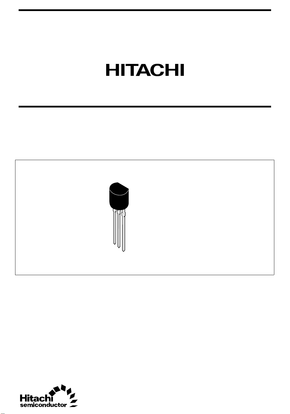
Outline
TO-92 (1)
2SD655
1. Emitter
2. Collector
3. Base
3
2
1
2SD655
Absolute Maximum Ratings (Ta = 25°C)
Item Symbol Ratings Unit
Collector to base voltage V
Collector to emitter voltage V
Emitter to base voltage V
Collector current I
Collector peak current i
Collector power dissipation P
CBO
CEO
EBO
C
C(peak)
C
Junction temperature Tj 150 °C
Storage temperature Tstg –55 to +150 °C
Electrical Characteristics (Ta = 25°C)
Item Symbol Min Typ Max Unit Test conditions
Collector to base breakdown
V
(BR)CBO
voltage
Collector to emitter breakdown
V
(BR)CEO
voltage
Emitter to base breakdown
V
(BR)EBO
voltage
Collector cutoff current I
Base to emitter voltage V
Collector to emitter saturation
V
CBO
BE
CE(sat)
voltage
DC current transfer ratio hFE*
Gain bandwidth product f
T
Notes: 1. The 2SD655 is grouped by hFE as follows.
2. Pulse test
DEF
250 to 500 400 to 800 600 to 1200
30 — — V IC = 10 µA, IE = 0
15 — — V IC = 1 mA, RBE = ∞
5——VI
— — 1.0 µAV
— — 1.0 V V
— 0.15 0.5 V IC = 500 mA, IB = 50 mA*
1
250 — 1200 V
— 250 — MHz V
30 V
15 V
5V
0.7 A
1.0 A
500 mW
= 10 µA, IC = 0
E
= 20 V, IE = 0
CB
= 1 V, IC = 150 mA
CE
= 1 V, IC = 150 mA*
CE
= 1 V, IC = 150 mA
CE
2
2
2
 Loading...