


HIT 2SD2123-S, 2SD2123-L, 2SD2122-S, 2SD2122-L Datasheet
2SD2122(L)/(S), 2SD2123(L)/(S)
Silicon NPN Epitaxial
Application
Low frequency power amplifier complementary pair with 2SB1409(L)/(S)
Outline
4
1
2
3
4
3
2
1
1. Base
2. Collector
3. Emitter
4. Collector
DPAK
S Type
L Type
2SD2122(L)/(S), 2SD2123(L)/(S)
2
Absolute Maximum Ratings (Ta = 25°C)
Ratings
Item Symbol 2SD2122(L)/(S) 2SD2123(L)/(S) Unit
Collector to base voltage V
CBO
180 180 V
Collector to emitter voltage V
CEO
120 160 V
Emitter to base voltage V
EBO
55V
Collector current I
C
1.5 1.5 A
Collector peak current I
C(peak)
33A
Collector power dissipation PC*
1
18 18 W
Junction temperature Tj 150 150 °C
Storage temperature Tstg –55 to +150 –55 to +150 °C
Note: 1. Value at TC = 25°C.
Electrical Characteristics (Ta = 25°C)
2SD2122(L)/(S) 2SD2123(L)/(S)
Item Symbol Min Typ Max Min Typ Max Unit Test conditions
Collector to base
breakdown voltage
V
(BR)CBO
180 — — 180 — — V IC = 1 mA, IE = 0
Collector to emitter
breakdown voltage
V
(BR)CEO
120 — — 160 — — V IC = 10 mA, RBE = ∞
Emitter to base
breakdown voltage
V
(BR)EBO
5——5——VI
E
= 1 mA, IC = 0
Collector cutoff current I
CBO
——10——10µAVCB = 160 V, IE = 0
DC current transfer ratio h
FE1
*
2
60 — 200 60 — 200 A VCE = 5 V, IC = 150 mA*
1
h
FE2
30 — — 30 — — VCE = 5 V, IC = 500 mA*
1
Collector to emitter
saturation voltage
V
CE(sat)
——1 ——1 V IC = 500 mA,
I
B
= 50 mA*
1
Base to emitter voltage V
BE
— — 1.5 — — 1.5 V VCE = 5 V, IC = 150 mA*
1
Gain bandwidth product f
T
— 180 — — 180 — MHz VCE = 5 V, IC = 150 mA*
1
Collector output
capacitance
Cob — 14 — — 14 — pF VCB = 10 V, IE = 0,
f = 1 MHz
Notes: 1. Pulse test
2. The 2SD2122(L)/(S) and 2SD2123(L)/(S) are grouped by h
FE1
as follows.
BC
60 to 120 100 to 200
2SD2122(L)/(S), 2SD2123(L)/(S)
3
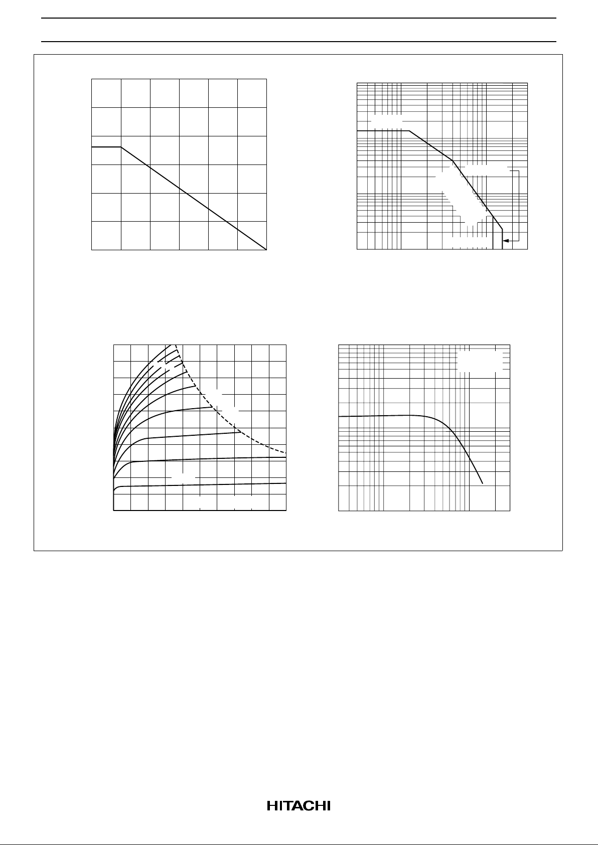
0
Case temperature T
C
(°C)
Collector power dissipation Pc (W)
Maximum Collector Dissipation Curve
50 100 150
10
30
20
0.01
0.03
0.1
0.3
1.0
3.0
10
Collector to emitter voltage V
CE
(V)
Collector current I
C
(A)
3 10 30 100 300
Area of Safe Operation
IC
(max)
DC Operation
(T
C
= 25°C)
2SD2123
2SD2122
Collector to emitter voltage VCE (V)
Collector current I
C
(A)
0
Typical Output Characteristics
10 20 30 40 50
0.2
0.6
0.8
1.0
0.4
IB = 0
P
C
= 18 W
TC = 25°C
1 mA
2
3
4
5
6
7
8
9
10
10
30
100
300
1,000
Collector current I
C
(A)
DC current transfer ratio h
FE
0.03 0.1 0.3 1.0 3.0
DC Current Transfer Ratio
vs. Collector Current
VCE = 5 V
Ta = 25°C