

HIT 2SD1366 Datasheet
Application
Low frequency power amplifier
Outline
UPAK
3
2SD1366
Silicon NPN Epitaxial
1
2
4
1. Base
2. Collector
3. Emitter
4. Collector (Flange)
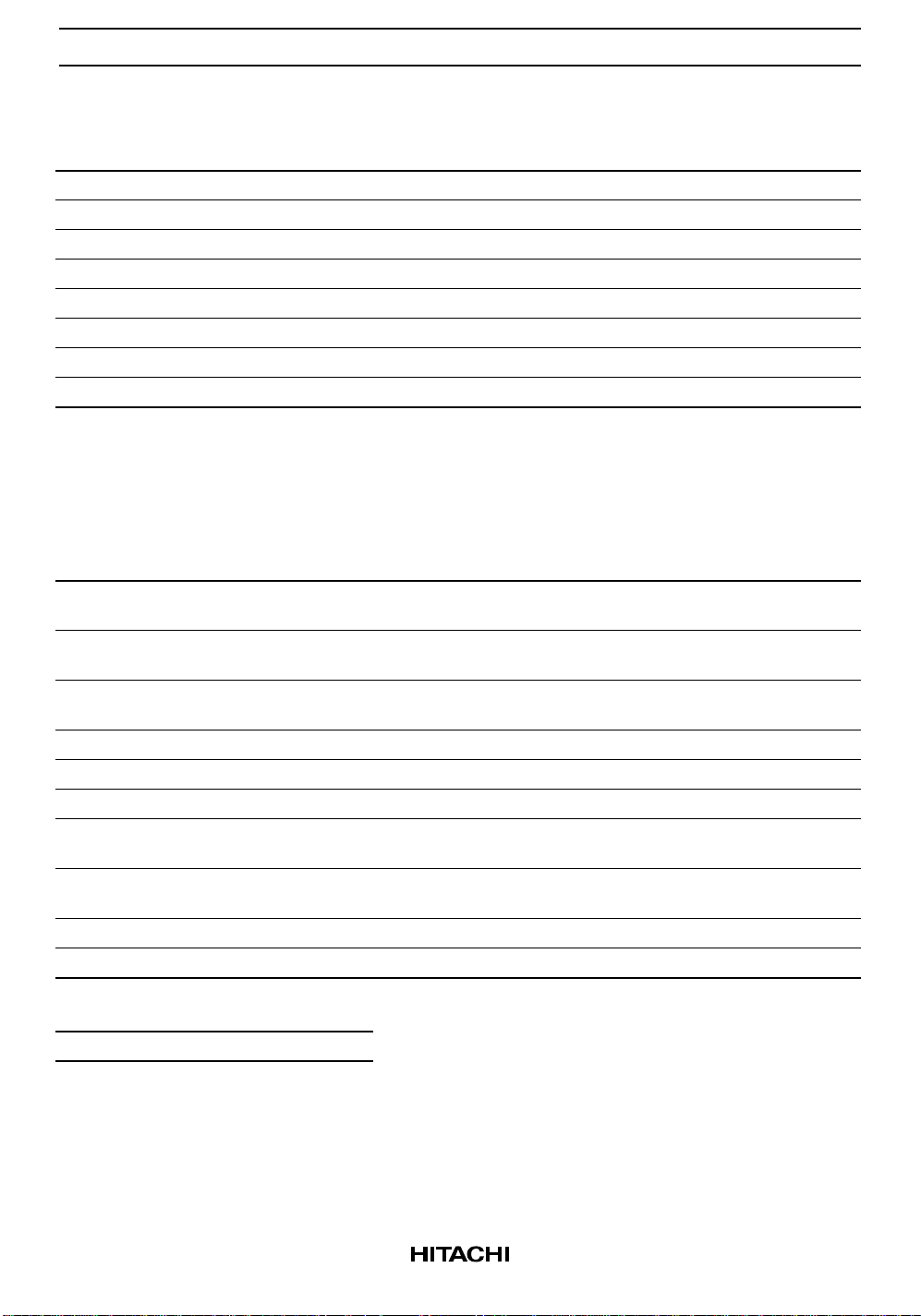
2SD1366
Absolute Maximum Ratings (Ta = 25°C)
Item Symbol Ratings Unit
Collector to base voltage V
Collector to emitter voltage V
Emitter to base voltage V
Collector current I
Collector peak current i
Collector power dissipation PC*
CBO
CEO
EBO
C
C(peak)
1
*
2
Junction temperature Tj 150 °C
Storage temperature Tstg –55 to +150 °C
Notes: 1. PW ≤ 10 ms, Duty cycle ≤ 20%.
2. Value on the alumina ceramic board (12.5 × 20 × 0.7 mm)
Electrical Characteristics (Ta = 25°C)
Item Symbol Min Typ Max Unit Test conditions
Collector to base breakdown
V
(BR)CBO
voltage
Collector to emitter breakdown
V
(BR)CEO
voltage
Emitter to base breakdown
V
(BR)EBO
voltage
Collector cutoff current I
Emitter cutoff current I
CBO
EBO
DC current transfer ratio hFE*
Collector to emitter saturation
V
CE(sat)
voltage
Base to emitter saturation
V
BE(sat)
voltage
Gain bandwidth product f
T
Collector output capacitance Cob — 22 — pF V
Note: 1. The 2SD1366 is grouped by hFE as follows.
Mark AA AB
h
FE
85 to 170 120 to 240
25 — — V IC = 10 µA, IE = 0
20 — — V IC = 1 mA, RBE = ∞
5——VI
— — 0.1 µAV
— 0.1 µAV
1
85 — 240 V
— 0.15 0.3 V IC = 0.8 A, IB = 0.08 A, Pulse
— 0.9 1.0 V IC = 0.8 A, IB = 0.08 A, Pulse
— 240 — MHz V
25 V
20 V
5V
1A
1.5 A
1W
= 10 µA, IC = 0
E
= 20 V, IE = 0
CB
= 4 V, IC = 0
EB
= 2 V, IC = 0.5 A, Pulse
CE
= 2 V, IC = 0.5 A, Pulse
CE
= 10 V, IE = 0, f = 1 MHz
CB
2
 Loading...