

Page 1

CONTENTS
1. X - RAY RADIATION PRECAUTION
2. SAFETY PRECAUTION
3. PRODUCT SAFETY NOTICE
4. THE ALIGNMENT FLOW CHART
5. INSTALLATION AND SERVICE ADJUSTMENTS
6. USA CHANNEL FREQUENCY TABLE (181 CH)
7. WIRING DIAGRAM
8. BLOCK DIAGRAM
9. IC BLOCK DIAGRAM
10. TDA9850 BLOCK DIAGRAM
11. COMPONENT AND BOTTOM VIEW
12. SCHEMATIC DIAGRAM
13. ELECTRICAL PARTS LIST
………………………………………………………. ……………
…………………………………………………………..……
………………………………………………………. ……..…………
………………………………………………………. ……...…….……
………………………………………………………. ……...………
………………………………………………. ……..….……
………………………………………………. …………..….……
………………………………………………. ………..….……
………………………………………………………
……………………………………………………..……
………………………………………………....……
…………………………………………
…………………………………...……
1
1
2
3
3
9
12
13
14
15
16
23
24
Page 2

CAUTION: BEFORE SERVICING THE CHASSIS, READ THE “X-RAY RADIATION
PRECAUTION” “SAFETY PRECAUTION” ON PAGE 1 AND “PRODUCT
SAFETY NOTICE” ON PAGE 2 OF THIS MANUAL.
X-RAY RADIATION PRECAUTION
1. Excessive high voltage can produce potentially hazardous X - RAY RADIATION. To avoid such
hazards, the high voltage must not be above the specified limit. The normal value of the high
voltage of this receiver is 28.5kV at zero beam current (minimum brightness) under a 120V AC
power source. The high voltage must not, under any circumstances, exceed 30kV.
2. Each time a receiver requires servicing, the high voltage should be checked following the HIGH
VOLTAGE CHECK procedure in this manual. It is recommended the reading of the high voltage
be recorded as a part of service record. It is important to use an accurate and reliable high voltage
meter.
3. This receiver is equipped with a Fail Safe (FS) circuit which prevents the receiver from
producing an excessively high voltage even if the B+ voltage increases abnormally. Each time the
receiver is serviced, the FS circuit must be checked to determine that the circuit is properly
functioning, following the FS CIRCUIT CHECK procedure in this manual.
4. The primary source of X - RAY RADIATION in this TV receiver is the picture tube. For
continuous X - RAY RADIATION protection, the replacement tube must be exactly the same type
tube as specified in the parts list.
5. Some parts in this receiver have special safety-related characteristics for X - RAY RADIATION
protection. For continuous safety, parts replacement should be undertaken only after referring to
the PRODUCT SAFETY NOTICE below.
SAFETY PRECAUTION
WARNING:
Service should not be attempted by anyone unfamiliar with the necessary precaution on this
receiver. The following are the necessary precautions to be observed before servicing this chassis.
1. Since the power supply circuit of this receiver is directly connected to the AC power line, an
isolation transformer should be used during any dynamic service to avoid possible shock hazard.
2. Always discharge the picture tube anode to the CRT conductive coating before handling the
picture tube. The picture tube is highly evacuated and if broken, glass fragments will be violently
expelled. Use shatter proof goggles and keep picture tube away from the unprotected body while
handling.
3. When replacing a chassis in the cabinet, always be certain that all the protective devices are put
back in place, such as: non-metallic control knobs, insulating covers, shields, isolation
resistor-capacitor network etc.
4. When replacing parts or circuit boards, disconnect the power cord.
5. When replacing a high wattage resistor (oxiode metal film resistor) on the circuit board, keep the
resistor 10mm (1/2in) away from circuit board.
6. Connection wires must be kept away from components with high voltage or high temperature.
7. If any fuse in this TV receiver is blown, replace it with the FUSE specified in the chassis parts
list.
- 1 -
Page 3
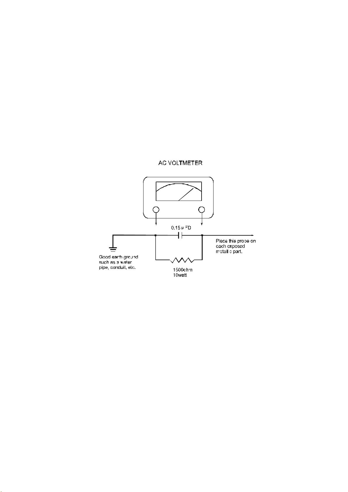
8. Before returning the set to your customer, always perform an AC leakage current check on the
exposed metallic parts of the cabinet, such as antennas, terminals, screwheads, metal overlays,
control shafts etc. to be sure the set is safe to operate without danger of electrical shock. Plug the
AC line cord directly into a 120V AC outlet (do not use a line isolation transformer during this
check). Use an AC voltmeter having 5000 ohms per volt or more sensitivity in the following
manner:
Connect a 1500 ohm 10 watt resistor, paralleled by a 0.15μF, AC type capacitor, between a known
good earth ground (water pipe, conduit, etc.) and the exposed metallic parts, one at a time. Measure
the AC voltage across the combination of 1500 ohm resistor and 0.15 μF capacitor. Reverse the
AC plug at the AC outlet and repeat AC voltage measurements for each exposed metallic part.
Voltage measured must not exceed 0.3 volts RMS. This corresponds to 0.2 milliamp. AC. Any
value exceeding this limit constitutes a potential shock hazard and must be corrected immediately.
PRODUCT SAFETY NOTICE
Many electrical and mechanical parts in the chassis have special safety-related characteristics.
These characteristics are often passed unnoticed by a visual inspection and the X-RAY
RADIATION protection afforded by them cannot necessarily be obtained by using replacement
components rated for higher wattage, etc. Replacement parts which have these special safety
characteristics are identified in this manual and its supplement electrical components having such
features are shaded on the schematic diagram and the parts list.
Before replacing any of these components, read the parts list in this manual carefully. The use of
substitute replacement parts which do not have the same char acteristic as specified in the parts list
may create shock, fire, X-RAY RADIATION or other hazards.
- 2 -
Page 4
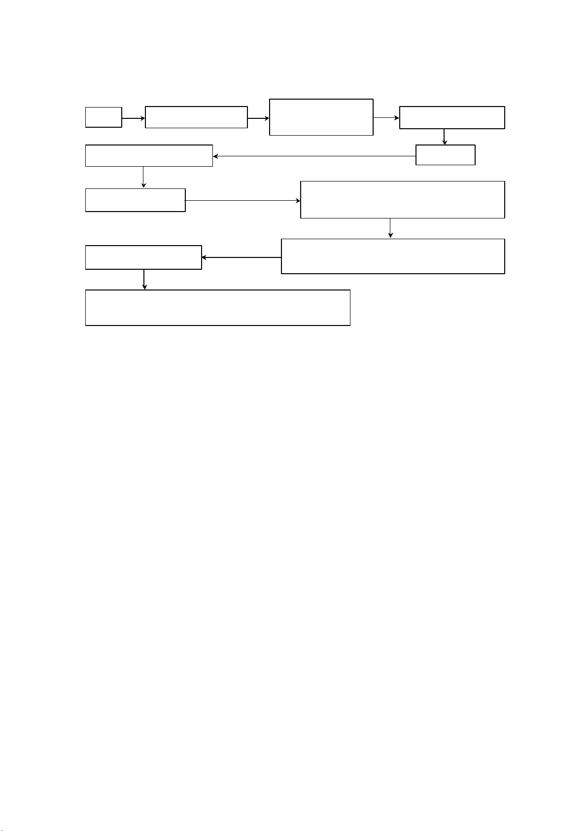
THE ALIGNMENT FLOW CHART
PIF
To fit the front cabinet,
Focus
alignment, focus, high
BTSC, secret code setting, AV function check.
Control buttons, channels, white balance, sound, hit the set
Factory items’ adjustment
Heatrun for 2 hours
To fit the back cabinet
B+, AGC,H-frequency
external degaussing
Preheat for 30 minutes
White balance revoltage,
X-ray protection test, sound power test, CCD, V-chip,
INSTALLATION AND SERVICE ADJUSTMENTS
GENERAL
In the majority of cases, a color television receiver will need only slight touch-up adjustment upon
installation. Check the basic characteristics such as FS、EHV and focus. Observe the picture for
good black and white details without objectionable color shading. If color shading is evident,
demagnetize the receiver.
If color shading still persists, perform purity and c onvergence adjustments. This should be all that is
necessary to achieve optimum receiver performance.
FOCUS ADJUSTMENT
Adjust the FOCUS control (on T471) for well defined scanning lines on the picture screen.
HIGH VOLTAGE CHECK
CAUTION: These is no HIGH VOLTAGE ADJUSTMENT on this chassis. Checking should be
done following the steps below.
1. Connect an accurate high voltage meter to the second anode of the picture tube.
2. Turn on the receiver. Set the BRIGHTNESS and CONTRAST controls to minimum (zero beam
current).
3. High voltage will be measured about 28.5kV.
4. Vary the BRIGHTNESS control to both extremes to be sure the high voltage does not exceed the
limit under any conditions.
FS CIRCUIT CHECK
The Fail Safe (FS) circuit check is indispensable for the final check in the servicing. Checking
should be done following the steps below.
- 3 -
Page 5
1. Turn the power switch on and adjust customer controls for normal operation.
Check that the set returns to normal operation when pin
34 of N101 on the Main Board is grounded with jumper
Power Circuit or Horizontal Circuit
Check if the voltage across capacitor
C411 is approximately 21V.
2. Temporarily short R412 on the Main Board with a jumper wire. Raster and sound will
disappear.
3. The receiver must remain in this state even after removing the jumper wire. This is the evidence
that the FS circuit is functioning properly.
4. To obtain a picture again, temporarily turn the receiver off and allow the FS circuit more than 30
seconds to reset. Then turn the power switch on to produce a normal picture.
Troubleshooting Guide for Fail Safe Circuit
YES NO
NO
YES
Faulty
Defective Fail Safe Circuit
PIF alignment
1) Apply DC 12V to output pin of N551(pin3 of N551 ) , connect pin7 of LA76814(N101)
to GND.
2) Apply 95dBμ, 45.75MHz RF signal to the tuner's IF pin through a 1000P ceramic
capacitor. Connect the DC voltameter's⊕pole to LA76814 pin 47 , ⊙ pole to GND.
Note: For LA76814 ES01 version, the voltameter's⊕pole should connect to pin50 .
3) Adjust T202 with a non-inductive screwdriver until the reading on the DC voltameter is DC
3.6V±0.01V.
B+ CHECK
1) Prepare the test equipment.
2) Use the DC voltameter at DC 200V position to test VD551⊕, i.e. B+.
3) Connect the power plug to AC 120V/60Hz, turn on the power switch, wait for normal raster,
then adjust RP551 to make B+ = 110V±0.5V.
Test point
VD551⊕ VD556⊕ VD554⊕ VD555⊕
DC(V) 110 25 15 18
- 4 -
Page 6

TEST EQUIPMENT
1) DC regulated power supply PAB18-1.8
2) Audio voltameter
3) Oscilloscope
4) High-voltage meter
5) Digital multimeter
6) AC voltameter
TEST MODE SET(CHECK)
TEST MODE ADJUSTMENT INSTRUCTION
TEST MODE adjustment is a special adjustment which is controlled by I2C BUS. The TV set has
been set at optimum mode at the factory. Except for special need, such as replacing CRT、
MEMORY 、IC etc., it is hoped not to adjust it. To conduct TEST MODE's adjustment, please do it
according to the following steps :
There are two special romote controller for the set. One is "Under Adjustment" and the other is
"Under Adjustment for W/B Balance".
1) Press "PROD" button to enter the FACTORY, B/W BALANCE, ADJUST or SETUP mode.
2) In B/W BALANCE mode, select the item you want to adjust directly by pressing the button on
the"Under Adjustment for W/B Balance" remote controller and use the "ADJ+" or "ADJ-" button
to adjust. You can press "ADJUP" or "ADJDOWN" to select needed adjustment item and use
the "ADJ+" or "ADJ-" button to adjust too.
3) In ADJUST mode, select the item you want to adjust directly by pressing the button on the "Under
Adjustment" remote controller and use the "ADJ+" or "ADJ-" button to adjust. You can press
"ADJUP" or "ADJDOWN" to select needed adjustment item and use the "ADJ+" or "ADJ-"
button to adjust too.
4) In SETUP mode, select the item you want to adjust by pressing the button "ADJUP" or
"ADJDOWN" on the "Under Adjustment". Then use the "ADJ+" or "ADJ-" button to adjust.
adjust.
5) Press "PROD" to exit the TEST MODE.
H-blanking, H-center adjustment
1) Receive test signal, enter into the ADJUST mode.
2) Select the H.BLK.LEFT and H.BLK.RIGHT item, adjust the level to make the H -blanking
amount on the left and right screen at an appropriate position.
3) Select the H.PHASE item, adjust the level to make the left and right picture sysmmetrical.
V-amplitude, linearity, S-correction, center adjustment
1) Receive test signal, enter into the ADJUST mode. adjust the value to make V-center and the CRT's
2) Select the V.POS item , adjust the value to make V-center and the CRT's geometric center is in
accordance. Then select the V.SIZE item, adjust the value to make the overscan is less than or
- 5 -
Page 7
Equate 10% .
2) Select the V.LINE item, adjust the value to make the upper and lower grid's(on the screen) vertical
distance equal. Select the V.SC item, adjustthe value to make the vertical distance from upper
grid to middle screen is equal to the vertical distance from lower grid to middle screen.
3) Repeat the above steps 2) &3) to make the V-center, V-amplitude, V-linearity at the optimum
mode.
White balance, sub-brightness adjustment
1) Receive test signal, enter into B/W BALANCE mode with the special remote controller of
"Under Adjustment for B/W BALANCE".
2) Set the value of item as the following table:
Name
Name
S-BRI
R-BIA
G-BIA
B-BIA
R-DRV
G-DRV
B-DRV
C.B/W
3) Set the value of S-BRI=85, then press "LINE" button. Adjust the SCREEN potentiameter
clockwise until a slight bright horizontal line appears on the screen. Adjust the value of
R-BIA, G-BIA and B-BIA, until the line change white. Press "LINE" button again. Then
decrease S-BRI to a proper value.
4) Press "LINE" button to exit B/W BALANCE mode.
Value
0~127
0~255
0~255
0~255
0~127
0~15
0~127
0~3
Default
-
-
-
-
65
7
65
0
Description
Sub Brightness
Red Bias
Green Bias
Blue Bias
Red Drive
Green Drive
Blue Drive
Cross B/W
ADJUST MENU LIST
Receive test signal, enter into ADJUST mode with the special remote controller of
"Under Adjustment".
Item
00*
01**
02**
03**
04*
05*
06*
07*
08**
09**
10**
11**
12
13
14
15
Name
H.PHASE
NT.H.PHASE
H.BLK.LEFT
H.BLK.RIGHT
V.SIZE
V.LINE
V.POSI
V.SC
NT.V.SIZE
NT.V.LINE
NT.V.POSI
NT.V.SC
RF.AGC
VOL.OUT
OSD.H.POSI
OSD.V.POSI
Description
H.PHASE
Vertical Size
Vertical Linearity
Vertical DC
Vertical S-Correction
RF AGC Delay
Volume Control
Value
0~31
0~31
0~7
0~7
0~127
0~31
0~63
0~31
-32~+31
-16~+15
-32~+31
-16~+15
0~63
0~127
0~127
0~31
Default
13
00
7
0
82
3
33
6
00
00
00
00
30
127
11
16
- 6 -
Page 8
16
17
18
19
21
22
INPUT LEVEL
SPECTRAL
WIDE BAND
STEREO
FILTER SET
SAP VCO
0~15
0~63
0~63
0~63
0~31
0~63
7
0
0
63
63
63
Note: 1.All the items sign with "*" can adjust to different value for different
TV set.
2.All the items sign with "**" do not affect the IC of La76814.
ADJUST MENU LIST
Receive test signal, enter into ADJUST mode with the special remote controller of
"Under Adjustment".
Item
00
01
02
03
04
05
06
07
08
09
10
11
12
13
14
15
16
17
18
19
20
21
22
23
24
25
26
27
28
29
30
31
32
33
34
35
Name
LA76814/LA76812
SAP IC SELECT
SUB.CONT
SUB.COLOR
SUB.SHARP
SUB.TINT
BLK.STR.DEF
AFC GAIN
V.SETUP
CD.MODE
DIGITALOSD
OSD CONT
GRAY MOD
B.GAMSEL
RG.GAM.DEF
FBPBLK.SW
BRIGHT ABL.TH
EMG.ABL.DEF
BRT.ABL.DEF
MID.STP.DEF
R-Y/B-Y G.BL
R-Y/B-Y ANG
C.KILL.OFF
SND.TRAP
VOL.FIL
VIF.SYS.SW
VIDEO.LEVEL
FM.LEVEL
POWER OPT
POWER FLAG
SEARCH CHECK
SEARCH SPEED
AV OPTION
POSITION L/R
BLUE BACK
BLACK BACK
Description
0:LA76814; 1:LA76812
0:TDA9850; 1:CXA2104; 2:TDA9855; 3:UPC1851B
Subcontrast(0~31)
Subcolor(0~63)
Subsharpness(0~31)
Subtint(0~63)
Black Stretch Definition(0:on; 1:off)
AFC Gain(0:low; 1:high)
Vertical Synchronization Separate Sense(0:low; 1:high)
Count Down Mode(LA76814:0/1;LA76812:0~7)
Digital OSD(0:Analog; 1:Digital)
OSD Contrast(0~127)/LA76814(0~3)
Gray Mode(0/1)
Blue Selection(0~3)
Red&Green Definition(0/1)
FBPBLK.SW(0/1)
Bright.Abl.Threshold(0~7)
Emg.Abl.Def(0/1)
Brt.Abl.Def(0/1)
Mid.Stp.Def(0/1)
R-Y/B-Y Gain Balance(0~15)(None for)(LA76814)
R-Y/B-Y Angle(0~15)
C_Kill OFF(0/1)
Sound Trap(0~7)
Volume Filter Defeat(0/1)
Video IF(0:45.75M;1:58.75M)
Video Level(0~7)
FM Level(31)
0:Twice On; 1:Memory; 2or3:Once On
0:No Power On Screen;1:Power On Screen
0:No Power On Search;1:Power On Search
0:Slow;1:Quick
AV Input (0:No; 1:1; 2:2; 3:3)
Position of CH Number(0:Upper Left;1:Upper Right)
Blue Back When No Signal(0:Off; 1:On)
Black Back When Switch Channel(0:Off;1:On)
Default
0
0
0
31
10
31
1
1
1
0
1
2
0
2
0
0
0
0
0
0
8
8
0
3
1
0
7
16
1
0
1
0
2
1
1
0
- 7 -
Page 9

STEREO OPTION
36
37
WOOFER/H.PHONE
38
WOOFER VOL.OPT
39
40
41
42
43
44
45
46
47
SENSITIVITY
V.MUTE P.OFF
CCD OPTION
V-CHIP OPTION
PASSWORD OPT
COMB.OPTION
TUNER OPTION
GAME OPTION
SCREEN OPTION
Stereo Option(0:off;1:on)
0:Woofer;1:Headphone
Volume of H.Phone(0:No Woofer;1:Woofer)
Sensitivity Function(0:off;1:on)
Cut Video Out Before Power Off(0:on; 1:off)
CCD Function(0:off; 1:on)
V-CHIP Function(0:off; 1:on)
Password of V-CHIP(0:off;1:on)
Y/C Separate Function(0:off;1:on)
0:TDF-3M3;1:PHOLIPUV1336B
Game Option(0:on; 1:off)
0:No Screen;1:Screen When Power On;2:ScreenWhen Power Off;3:Screen When Power On/Off
1
0
0
0
0
1
1
1
0
1
1
0
- 8 -
Page 10

USA CHANNEL FREQUENCY TABLE
U.S.A. Channel
PIF 45.75MHZ, CIF 42.17MHZ, SIF 41.25MHZ.
UNIT:MHZ
Channel fp(picture) fs(sound) Channel fp(picture) fs(sound)
2 55.25 59.75 36 603.25 607.75
3 61.25 65.75 37 609.25 613.75
4 67.25 74.75 38 615.25 619.75
5 77.25 81.75 39 621.25 625.75
6 83.25 87.75 40 627.25 631.75
7 175.25 179.75 41 633.25 637.75
8 181.25 185.75 42 639.25 643.75
9 187.25 191.75 43 645.25 649.75
10 193.25 197.75 44 651.25 655.75
11 199.25 203.75 45 657.25 661.75
12 205.25 209.75 46 663.25 667.75
13 211.25 215.75 47 669.25 673.75
14 471.25 475.75 48 675.25 679.75
15 477.25 481.75 49 681.25 685.75
16 483.25 487.75 50 687.25 691.75
17 489.25 493.75 51 693.25 697.75
18 495.25 499.75 52 699.25 703.75
19 501.25 505.75 53 705.25 709.75
20 507.25 511.75 54 711.25 715.75
21 513.25 517.75 55 717.25 721.75
22 519.25 523.75 56 723.25 727.75
23 525.25 529.75 57 729.25 733.75
24 531.25 535.75 58 735.25 739.75
25 537.25 541.75 59 741.25 745.75
26 543.25 547.75 60 747.25 751.75
27 549.25 553.75 61 753.25 757.75
28 555.25 559.75 62 759.25 763.75
29 561.25 565.75 63 765.25 769.75
30 567.25 571.75 64 771.25 775.75
31 573.25 577.75 65 777.25 781.75
32 579.25 583.75 66 783.25 787.75
33 585.25 589.75 67 789.25 793.75
34 591.25 595.75 68 795.25 799.75
35 597.25 601.75
69 801.25 805.75
-9-
Page 11

USA CHANNEL FREQUENCY TABLE
U.S.A. CATV Channel
PIF 45.75MHZ, CIF 42.17MHZ, SIF 41.25MHZ.
UNIT:MHZ
Channel fp(picture) fs(sound) Channel fp(picture) fs(sound)
1 73.25 77.75 36 295.25 299.75
2 55.25 59.75 37 301.25 305.75
3 61.25 65.75 38 307.25 311.75
4 67.25 74.75 39 313.25 317.75
5 77.25 81.75 40 319.25 323.75
6 83.25 87.75 41 325.25 329.75
7 175.25 179.75 42 331.25 335.75
8 181.25 185.75 43 337.25 341.75
9 187.25 191.75 44 343.25 347.75
10 193.25 197.75 45 349.25 353.75
11 199.25 203.75 46 355.25 359.75
12 205.25 209.75 47 361.25 365.75
13 211.25 215.75 48 367.25 371.75
14 121.25 125.75 49 373.25 377.75
15 127.25 131.75 50 379.25 383.75
16 133.25 137.75 51 385.25 389.75
17 139.25 143.75 52 391.25 395.75
18 145.25 149.75 53 397.25 401.75
19 151.25 155.75 54 403.25 407.75
20 157.25 161.75 55 409.25 413.75
21 163.25 167.75 56 415.25 419.75
22 169.25 173.75 57 421.25 425.75
23 217.25 221.75 58 427.25 431.75
24 223.25 227.75 59 433.25 437.75
25 229.25 233.75 60 439.25 443.75
26 235.25 239.75 61 445.25 449.75
27 241.25 245.75 62 451.25 455.75
28 247.25 251.75 63 457.25 461.75
29 253.25 257.75 64 463.25 467.75
30 259.25 263.75 65 469.25 473.75
31 265.25 269.75 66 475.25 479.75
32 271.25 275.75 67 481.25 485.75
33 277.25 281.75 68 487.25 491.75
34 283.25 287.75 69 493.25 497.75
35 289.25 293.75
70 499.25 503.75
-10-
Page 12

USA CHANNEL FREQUENCY TABLE
U.S.A. CATV Channel
PIF 45.75MHZ, CIF 42.17MHZ, SIF 41.25MHZ.
UNIT:MHZ
Channel fp(picture) fs(sound) Channel fp(picture) fs(sound)
71 505.25 509.75 99 115.25 119.75
72 511.25 515.75 100 649.25 653.75
73 517.25 521.75 101 655.25 659.75
74 523.25 527.75 102 661.25 665.75
75 529.25 533.75 103 667.25 671.75
76 535.25 539.75 104 673.25 677.75
77 541.25 545.75 105 679.25 683.75
78 547.25 551.75 106 685.25 689.75
79 553.25 557.75 107 691.25 695.75
80 559.25 563.75 108 697.25 701.75
81 565.25 569.75 109 703.25 707.75
82 571.25 575.75 110 709.25 713.75
83 577.25 581.75 111 715.25 719.75
84 583.25 587.75 112 721.25 725.75
85 589.25 593.75 113 727.25 731.75
86 595.25 599.75 114 733.25 737.75
87 601.25 605.75 115 739.25 743.75
88 607.25 611.75 116 745.25 749.75
89 613.25 617.75 117 751.25 755.75
90 619.25 623.75 118 757.25 761.75
91 625.25 629.75 119 763.25 767.75
92 631.25 635.75 120 769.25 773.75
93 637.25 641.75 121 775.25 779.75
94 643.25 647.75 122 781.25 785.75
95 91.25 95.75 123 787.25 791.75
96 97.25 101.75 124 793.25 797.75
97 103.25 107.75 125 799.25 803.75
98 109.25 113.75
-11-
Page 13

- 12 -
Page 14

V
OUT
IDE
O
V
I
D
IN
E
O
AU
IN
D
IO
AU
O
U
DI
T
O
I
N
1
IN2
LA
4
28
7
TC4
SW
0
53
I
TC
B
P/
H
BF
A
MP
A
U
D
IO
T
DA
985
0
A
NTS
C
1
2
C
0V
MU2
IR
8
P038
TX
1
BT
S
C
25
V
2SC
V5
4
13
2
3
7
IN
OU
T
OU
T
B
8
P
1
6
V
OWER
1
8V
13
0V
V
ID
E
O
FM
B
3
B
2
B1
I
R RX
G
B
D
RI
V
E
C
RT
C
R
T
CH
R
O
MA
R
BLOCK DIAGRAM
LC
LC
C
C
P
AT
2
4C
0
4
SIF
P
8
8
U
U
6
6
323
323
N70
N70
2A
2A
1
1
N
7
0
2
3D
D
25
5
3
M
EM
ORY
V
43
2
VI
D
EO
H
O
U
T
F
B
T
PI
F
T
4
7
1
T
U
N
E
R
S
S
A
A
W
W
F
F
A1
0
1
L
A7
8
4
1
Z
2
0
1
D
EFL
EC
T
IO
N
N
V O
4
51
U
T
N1
0
1
L
A
76
8
1
4
- 13 -
Page 15

LA76814IC BLOCK DIAGRAM
AudioOutput
FMOutput
PIFAGCFilter
RFAGCOutput
PIFInput1
PIFInput2
IFGround
IFVcc
FMFilter
AFTOutput
BusData
BusClock
ABL
2.5
2.5
2.53
2.56
2.8
2.8
5V
2.12
2.34
4.8
4.8
3.52
3
SIFInput
2.4
SIFAPCFilter
1.93
SIFOutput
2.11
Ext.AudioInput.
2.3
FLLFilter
4
VCOCoil1
4
VCOCoil2
3.7
APCfilter
2.18
VideoOutput
2.53
BlackLevelDetector
2.7
InternalVideoInput(S_CIN)
Video/VerticalGround
5V
2.4
ExternalVideoInput(YIN)
RedInput
GreenInput
BlueInput
FastBlankingInput
RGBVcc
RedOutput
GreenOutput
BlueOutput
B.AKBInput
Vertical
Output
RAMPALC
Filter
Holizontal/Bus
HolizontalAFC
Holizontal
Vcc
Filter
Output
1.1
1.15
1.13
0
8
3.16
3.16
3.05
0
2.51
2.63
5V
2.63
0.48
Video/Vertical/BUSGround
0
2.32
SelectedVideoOutput
3.06
ACCFilter
2.64
3.58MHzCrystal
0.53
fsc(3.58MHz)Output
3.3
ChromaAPC1Filter
0.35
KillerFilter
0
X-RAY
HolizontalGround
0
2.9
OSDContrast
NC
NC
1.7
VCOIREF
1.11
FBPInput
- 14 -
Page 16

C13
C12 C11
C16
C15
C17 C14
composite
baseband
input
C1
+
11
+
5
4
DEMODULATOR
SAP
ADJUST
INPUT
LEVEL
DETECTOR
STEREODECODER
C3
R1
+
+
C2
C4
C5
NOISE
Q1
+
+ + + + +
R3
326
R2
21
DBX
STEREO/SAP
SWITCH
TDA9850
1713 14 15 16
ceramic
resonator
onlyduring
adjustment
VrefV CAPVCC
C10 C9 CL CR
C19 C18
SDA
SCL
L-R/SAP
SELECT
MODE
+
21
OUTR
SAP
to
audio
processing
L+R
DEMATRIX
18 19
27
OUTL
stereo
mono
C6 C7
+
+
303132
29
STEREO
ADJUST
+
102025
SUPPLY
12
DE-EMPHASIS
23
22
C8
SAPwithoutDBX
MHA010
6
24
8
9
TRANSCEIVER
LOGIC,IC-
2
28
7
MAD
++
- 15 -
Page 17

COMPONENT VIEW OF MAIN BORAD
- 16 -
Page 18

Page 19

Page 20

COMPONENT VIEW OF CRT BORAD
- 18 -
Page 21

COMPONENT VIEW OF STEREO BORAD
- 20 -
Page 22

NISPT-2
U902
AC110V
60HZ
233-3.15A/125V
1/2DJ220K
F501
R501
LIVE AREA
DJ22K
R515
C515
FJ0.01
400KM2200S
OMIT-SS-112LM
C533
RL551
1/2W5.6M
R531
VD553
10V470
1N4148
12V
B6
AN7805
N552
1
2
C572
3
+
B7
5V
10V470
25V2200
2SJ1.5K
+
C570
B5
5V
CIRCUIT DIAGRAM OF MODEL TC14FS68
C407
50V1
R402
3.3K
R408
2.2K
R499
4.7K
680
R413
10K
1N4148
VD401
VD402
1N4148
+
C408
50V0.47
R403
330K
+
35V1000
C302
R305
1K5
R306
56K
R307
2.2K
2.7K
R311
1N4148
VD301
3DD3852
components replacement pointed out by the
mark.
6.This circuit diagram covers a basic or
representative chassis only.There may be
some comonents or partial circuit
differences between the acutal chassis
and the circuit diagram.
+
35V47
C301
8.2K
R301
100K
R302
C303
FK0.082
270K
R303
10K
R304
2SC1815Y
V301
FK0.082
C304
RP301
B-50K
PCC H-W
RP302
B-10K
R308
68K
R309
56K
R310
2.7k
2SA1015Y
V302
C315
1000
V303
have special signficance to product safety. It
is particularly recommended that only the
parts specified in service manual be used for
1/2SJ560
+
35V470
C306
DJ5.6K
R312
2W4.7
R313
5.Product safety should be considered when a
component replacement is made in any area
of receiver.The values of components
indicated by a mark in this circuit diagram
QHXC-73Q
L909
1
2
2
00
0
VD514
D
15K
R522
R524
B8
4.7K
R553
UZ6.2BSB
VD561
20
G OUT
KILLER FLT
35
22K
R411A
JDT1904
T431
Z2073
L433
0
00
PTDCA1BF3R0Q100
RT501
HF2836
L502
250V220
C507
5W6.8
7
8
1KV470
C556
2KV470
RP551
B-2K
2SC1815Y
V553
R554
150K
R556
22K
+
16V47
C244
C245
0.01
19
R OUT
APC1 FIL36FSC OUT
C207
FK0.01
50V0.47
C208
2M
+
R205
R206
47K
25V
+
50V10
C434
2SD1879
V432
1
TJC2-2A
+
1W100K
R520
1KV2700p
C516
R525
9
C551
+
1/2DJ100K
1/2DJ47K
R555
270
18
VCC (RGB)
37
R268
1K
R207
B8
2W220
R434
XS501
1000KM1000p
C504
1000KM1000p
C506
500K1000p
C518
BCK-42-25
3
10
RU4AM
160V220
C561
2SJ47K
R551
R552
1N4148
VD552
R243
17
XTAL
38
C209
J
S3.58
G201
16V0.47
R232
10K
C231
50NP1
T511
VD551
ACC FIL
+
C210
C532
HF2836
250HM0.1
C501
R517
100
2SC3807
V512
+
C565
2FJ1
R562
R568
18V
B2
N553
AN7805
1
2
3
1/2DJ270
+
FK0.068
C406
26
27
H AFC FIL
H OUT
VCO IREF
FBP IN
29
28
3K
R273
4.7K
R409
0.01
UZ5.6BSB
VD499
R404
820
24V
R314
160V47
4.The rated voltage of all capacitance is 50 V
unless otherwise rated.
F.
represents
F,n represents nF.
400KM470p
L501
250HM0.1
C502
7WK1
2SA1015
5.6K
V511
VD516
1N4148
2.2K
R526
2
13
14
VD555
EU2
R567
1.2K
2SC1815Y
V552
R561
10K
R400
FK0.47
C403
FK0.22
+
16V220
C404
C405
2.2K
0.01
4700P
TEM2011
C499
L401
24
25
RAMP ALC.FIL
VCC (H)
CLOCK OUT
VCC (CCD)
30
31
16V10
R272
4.7K
C279
3K
C431
X
C433
500KK3900
400NJ0.033
C437
B4
C305
VD436
RU4C
L301
600uH
2.The rated power of all resistance is 1/6W
unless otherwise noted.
3.All capacitance values without unit are in
R502
R511
VD517
EU1
15
FK0.1
R519
C514
1KV4700P
C520
5W47
2SC4237
V513
1
11
12
1KV470
C554
ES1
VD556
RU4AM
VD554
+
50V220
C566
+
25V1000
C564
1FJ2.2
R569
25V
R566
10K
2SB764
V554
1
2
3
3W39
R563
AN7812
N551
12V
B6
50V0.47
C401
+
C402
R244
2.7K
R401
21
22
23
B OUT
AKB IN
V OUT
OSD CONTRAST
GND (CCD/H)
X-RAY
32
34
33
R414
10K
C276
+
R274
R275
C274
0.01
C412
50V1
+
UZ7.5BSB
VD412
R415
3.9K
8.2K
R412
+
35V47
C411
1/2W3.3
VD411
EU1
R432
J
2SC2383-O
V431
R433
1/2SJ1K
C432
500KK1000
ZZ008
L431
ZZ008
L432
2000MJ1500
C435
2000MJ9200
C438
RU4DS
VD435
NOTICE:
1.All resistance values are in ohms.K represents
K
, M represents M
.K=10E3,M=10E6
TA30-10
VD504
VD506
TA30-10
43
N501
PC817B
OMIT-SS-112M
RL552
SEL VIDEO OUT
39
H-PULSE
ABL
TEST
TEST
R233
1/2W1.5K
TA30-10
VD503
TA30-10
VD505
1
2
130V
40
TP-G
JF0501-91802
TP-H
1000KM1000p
1000KM1000p
B1
GND (V/C/B)
41
50V1
C212
X
T471
C503
C505
R242
100
12
ABL13R IN14G IN15B IN16BLANK IN
EXT VIDEO IN
VCC (V/C/D)
43
42
0.01
C205
+
16V47
C206
+
24V
35V100
C472
+
130V
B1
R472
2
1
8
X
R241
100
C204
50V1
B4
EU2
1FJ1
2SC1815Y
R733
47K
100K
R114
C118
0.01
AFT OUT
DATA11CLOCK
BLK STRETCH FIL
INT VIDEO IN
44
+
+
C203
16V4.7
VD472
R472
SCREEN
FOCUS
10K
10
45
76543
R732
3.3K
50V1
560K
1.2K
V705
R730
R120
C117
R204
R202
9
2SC1815Y
V703
2SC1815Y
V704
R729
150K
R113
100K
+
9
FM FIL
VIDEO OUT
46
R201
1K
+
50V0.47
C137
10
1FJ1
EU1
HV
250V22
TRL-R
W700
J
R721
10K
R736
4.7K
L102
22UH
+
16V100
C115
C116
0.01
8
VCC (VIF)
APC FIL
47
220K
R474
VD474
+
C474
SCN-4Y
VD701
W704
X
470
10K
10K
21
V SYNC
H SYNC
R OUT22G OUT
R738
4.7K
B7
5V
38M
7
VIF IN2
GND(IF)
VCO COIL48VCO COIL
T101
200FK0.33
C441
+
R446
160V4.7
C444
1/2SJ1K
1FJ3.3
R491
2
2
TUNER
R774
C772
R758
5V
+
C733
R630
INPUT
A101
+
C103
50V2.2
R102
100K
12K
6
VOL-R
MUTE
37
22K
B5
V632
2SC1815Y
PUMP OUT
NON INPUT
OUTPUT
AGC
R776
10K
KK470
R759
8.2K
560
LA7841
XS701
1K
R772
R770
100
C771
5
VOL-L
AV238AV1
10K
R777
R778
N451
NC
R103
12K
W-VOL
R760
JPP2197BCS32
SDA
100
12V
R773
R735
10K
3
4
AV/TV
39
40
R761
22K
16V100
1N4148
VD610
16V100
K6D
SCL
R105
B6
22K
2.2K
+
C612
1N4148
+
C622
SCN-4Y
1
1
2
2
3
3
4
4
R748
R762
VD611
16V100
V-MUTE
XP901
C101
0.01
100
22K
41
22K
16V/2.2
0.01
1N4148
FO
+
C102
5V
R104
16V100
1N4148
C627
VD621
16V10
16V470
50V0.47
D
5V
5V
R101
33KB7
5V
R746
LNA150/602ALARM
COMB-FILTER
42
R763
22K
22K
+
C613
VD612
+
C628
16V100
1N4148
+
C931
C933
+
C934
+
VD933
2KV1000
CW574CS
50V4.7
C708
B5
R764
R765
16V/2.2
C618
0.01
1N4148
+
C623
VD622
12V
B6
R935
39
C939
N705
+
VD620
7
7
1
1
33V
+
C617
R727
470
UZ3.6BSB
VD703
R723
8.2K
2SA1015Y
V702
R728
R734
C729
0.01
R731
270K
R726
16V2.2
C714
+
R725
C713
50V1
330
+
17
19
20
RESET
FILT18CVBS-IN
BLANK
B OUT
23
24
R740
4.7K
0.01
R109
1K
R111
82
5
6
VIF IN1
VCO FIL
49
50
R128
X
C140
470
+
R442
R441
XS401
3.3K
3.3K
C110
0.01
0.01
D45U
50V1
50V0.47
220
2140
R742
R743
C112
C119
C136
L442
NC
25
220
2SC2216
V102
Z101
1K
FK0.022
C120
4
PIF AGC
RF AGC
EXT AUDIO IN
SIF OUT
51
+
C139
R127
L441
+
16V100
C450
12V
B3
26
R745
0.68UH
R119
3
52
1000
3K
12K
1SJ1
5.6K
220
L101
R454
R453
SDA0
SDA
R108
R110
C121XC122
FM OUT
SIF APC FIL
C123
R459
R722
1.5K
R724
4.7K
R720
10K
27
R747
22K
4
AT24C04
SCL
5
0.01
100
12V
B3
X
2
53
+
C124
50V1
R121
1K
1K
1/2DJ120
R461A
10K
0.01
LC863232A
SCL0
28
22K
2 3
N702
GND
6
R744
220
C111
R107
1
AUDIO OUT
SIF IN
54
15UH
1000
R455
12K
R458
50V1
25V2200
TJC2-5Y
N701
R749
7
5.6K
R708
C703
AFT IN
SDA1
VCC
LA76814
L121
R451
C453
+
C456
+
C457
XP402
150K
27K
8.2K
3.9K
2.7K
14NC15NC16
29
R751
22K
1
8
N101
330
153
153
4.7K
1.5K
680
39
18
12K
39K
R700
R701
R702
R703
R704
R705
R706
R707
16V47
13
SCL1
30
16V47
0.01
C126
C125
R122
35V1000
50V1
R456
R457
100FK0.1
2
2
0.01
22K
1W1R
C454
1Z75
+
C701
C702
R753
+
C719
C720
R451A
C452
+
+
2W270
C458
VDD12KEY IN
SAFTY
24V
VD452
R460
B5
5V
SW701
CH+
SW702
CH-
SW703
VOL+
SW704
VOL-
SW705
MENU
SW706
AV/TV
L701
39UH
C704
15P
C705
18P
G701
32K
390K
R709
10
11
XTAL2
S-VHS
NC
33
31
32
R754
10K
R755
R756
22K
22K
R602
1K
2SC1815Y
V601
R116
100
16V/100
C631
+
VD631
D
B4
35V100
EM01Z
VD451
C451
+
500FK10
C455
R452
1
100FK0.1
C459
4
4
XS402
TJC2-5A
GND9XTAL1
IR
34
100
B10K
RP601
10K
SRS ON/OFF
35
R766
22K
HS-0038
A701
5V
2SC1815Y
V633
R632
V631
2SA1015Y
7
6
5
4
3
2
1
R775
10K
100
KK470
7NC8
POWER
WOOFER ON/OFF
36
R757
22K
B7
R779
8.2K
+
C734
16V/10
R780
560
16V/10
R631
10K
10K
VCC2
VCC1
GND
130V
B1
3W10K
R718
IF
16V10
C611
+
R611
680
C621
16V10
680
25V/470
C615
+
12V
B3
XS403
SCN-5
XP902
SCN-5Y
54321
L901
10UH
DJ10K
R900
V932
2SC
R940
33
10
10
9
6118
6118
9
A59QDF891X002
U901
+
R621
25V470
C625
1.5K
C821
50V1
R821
1K
C819
220
+
2.2
R933
16V10
W902 JG0034
+
2SC
R822
4.7K
1
2
3
4
5
6
7
8
9
10
1
2
3
4
5
6
7
8
9
10
R615
63V0.1
C616
R931
1K
R932
15K
C932
+
V931
2SA
XP903
TJC2-2A
GZS10-2-AC2DG
XS901
B7
5V
V821
100K
R804
16V470
C805
+
12V
R610
R622
R924
CJ56R
0.01
16V220
C923
2SC
27K
C802
+
C801
16V10
1K
18V
63V0.1
C626
TJC3-2A
TJC3-2Y
5W8OHM
V801
R801
+
C814
SDA
SCL
AUDIO
Rout
Lout
R620
B2
XS602
XP602
B902
100
V922
2SC2688
R928
1/2SJ2.7K
B3
B7
5V
16
15
14
1X
13
OX
12
A
11
B
10
C
9
0.01
R922
CJ390
680
2SJ10K
R927
R803
220
50V1
C803
R802
68K
+
R823
68K
R612
3K
1K
3K
INT
GND
EXT
N601
SW
VOL
LA4285(R)
FLI
NFB
GND
OUT
VCC
INT
GND
EXT
SW
N602
VOL
FLI
LA4285(L)
NFB
GND
OUT
VCC
+
C606
25V1000
C607
0.01
R625
2.2
TJC3-3A
XS601
TJC3-3Y
XP601
5W8OHM
B901
330
CJ390
C921
R926
680
VD921
D
50V1
VDD
Y COM
X COM
C804
C911
R916
C822
+
TC4053BP/BF
50V1
50V1
50V10
50V10
50V10
100nF
50V2.2
16V100
15nF
50V10
50V2.2
50V4.7
50V4.7
B503F58
Q01
R914
330
CJ56R
VD911
D
16V10
C823
R833
220
R832
68K
N801
2SC1815Y
C12
+
C11
+
C10
+
C09
+
C20
+
C17
CL
+
C18
+
C08
C21
+
CR
+
C07
+
C06
+
C913
R918
1/2SJ2.7K
+
27K
V803
2SC2688
R834
100
12V
B3
V802
2SC
R831
27K
50V1
1Y
1
0Y
2
1Z
3
Z COM
4
OZ
5
INH
6
VEE
7
VSS
8
82
+
16V10
C813
VD801
D
R824
R820
3.3K
R819
1K
Rout
Lin
Rin
Lout
Cs
32
Cw
31
Cts
30
Ctw
29
MAD
28
OUTL
27
Cnd
26
Cl
25
Vref
24
SAP
23
Csde
22
OUTR
21
Cr
20
Css
19
Cmo
18
CER
17
R904
330
R912
100
V912
CJ390
2SJ10K
CJ56R
C901
560
R906
VD901
D
1/2SJ2.7K
R908
R917
R838
100
16V10
C825
+
R837
220
V803
2SC
16V10
4.7K
B7
12V
2SC2688
68K
16V10
+
C807
+
C808
16V10
C809
+
+
+
R815
B6
VEO
VEI
Cnr
Cm
Cdec
AGND
DGND
SDA
SCL
Vcc
COMP
Vcap
Cp1
Cp2
Cph
Cadj
TDA9850
100
V902
2SJ10K
16V10
R902
16V10
1
2
3
4
5
6
7
8
9
R835
27K
R836
R808
82
R810
47K
R809
4.7K
47K
R811
4.7K
4.7K
R814
47K
R813
R805
4.7K
R806
47K
C810
C811
X
VHS
R817
82
C812
0.01
R816
8.2K
12V
B6
RJ8.2K
R02
47nF
C13
RJ160
R03
+
50V10
C14
100nF
C15
+
50V4.7
C16
R21
100
R20
100
10
+
11
50V10
C01
+
12
16V100
C19
13
470nF
C02
50V4.7
2.2K
R01
C03
14
+
C04
15
220nF
+
16
50V10
C05
N641
R907
C824
+
R818
5V
C903
12V
B3
R807
82
16V10
C806
+
R812
W801
82
+
16V100
39
CRT BOARD
XS801-2
Vout
AVout
Lout
Rout
XS803
V1in
AV1
L1in
R1in
XS801-1
AV2
V2in
L2in
R2in
XS802
Y
C
R825
C00
R00
12V
B6
Page 23

PARTS LIST FOR TC14FS68
NO DESCRIPTION UNIT QTYLOCATION
PCB
1 E/RSAG7.820.041 PCS 1 A1 (THE MAIN PCB)
2 E/RSAG7.820.304A PCS 1 A2 (THE CONTROL PCB)
3 E/RSAG7.820.291A PCS 1 A4 (THE FRONT AV PCB)
4 E/RSAG7.820.042 PCS 1 A5 (THE STEREO PCB)
5 E/RSAG7.820.036 PCS 1 A6 (THE CRT PCB)
1/6W CARBON RESISTOR
6 RT13-1/6W-2R2-J PCS 2 R615 R625
7 RT13-1/6W-75R-J PCS 2 W805 R803
8 RT13-1/6W-82R-J PCS 5 R817 R818 R825 R1801 R1802
9 RT13-1/6W-100R-J PCS 12 R116 R241 R242 R766 R770 R774 R834 R838 R804 R902
R912 R922
10 RT13-1/6W-220R-J PCS 7 R127 R744 R745 R833 R837 R03 R02
11 RT13-1/6W-270R-J PCS 1 R243
12 RT13-1/6W-330R-J PCS 5 R122 R725 R904 R914 R924
13 RT13-1/6W-470R-J PCS
14 RT13-1/6W-560R-J PCS 3 R778 R780 R906
15 RT13-1/6W-680R-J PCS 6 R409 R707 R611 R621 R916 R926
16 RT13-1/6W-820R-J PCS 1 R404
17 RT13-1/6W-1K0-J PCS 15 R103 R119 R121 R201 R268 R458 R602 R821 R610 R620 R931 R104 R105 R612 R622
18 RT13-1/6W-1K2-J PCS 2 R202 R567
19 RT13-1/6W-1K5-J PCS 3 R722 R1707 R933
20 RT13-1/6W-2K2-J PCS
21 RT13-1/6W-2K7-J PCS 3 R244 R1706
22 RT13-1/6W-3K0-J PCS 3 R272 R275 R454
23 RT13-1/6W-3K3-J PCS 4 R402 R742 R743 R820
24 RT13-1/6W-3K9-J PCS 2 R1705 R415
25 RT13-1/6W-4K7-J PCS 20 R274 R724 R736 R738 R740 R809 R811 R813 R814 R815 R816 R822 R827
2 R727 R728
3 R401 R408 R760
R1704 R1805 R1806 R747 R749 R751 R753
27 RT13-1/6W-8K2-J PCS 6 R412 R723 R777 R779 R826 R1703
28 RT13-1/6W-10K-J PCS 24 R414 R561 R566 R630 R631 R632 R708 R720 R721 R730 R731
R733 R734 R735 R754 R772 R775 R819 R232 R413 R499 R755 R761 R762
29 RT13-1/6W-12K-J PCS 4 R453 R455 R773 R776
30 RT13-1/6W-15K-J PCS 1 R932
31 RT13-1/6W-22K-J PCS 10 R205 R746 R748 R756 R757 R758 R759 R763 R764 R765
32 RT13-1/6W-27K-J PCS 5 R801 R824 R831 R835 R1702
33 RT13-1/6W-33K-J PCS 2 R101 R120
35 RT13-1/6W-47K-J PCS 2 R206 R732
37 RT13-1/6W-68K-J PCS 4 R802 R805 R832 R836
Page 1 of 22
Page 24

NO DESCRIPTION UNIT QTYLOCATION
38 RT13-1/6W-100K-J PCS 3 R102 R113 R114
39 RT13-1/6W-150K-J PCS 2 R729 R1701
40 RT13-1/6W-270K-J PCS 1 R726
41 RT13-1/6W-330K-J PCS 1 R403
42 RT13-1/6W-390K-J PCS 1 R709
43 RT13-1/6W-560K-J PCS 1 R204
44 RT13-1/6W-2M0-J PCS 1 R207
1/4W CARBON RESISTOR
45 RT14-1/4W-15R-J PCS 1 R519
46 RT14-1/4W-33R-J PCS 2 R935 R940
47 RT14-1/4W-56R-J PCS 1 R01
48 RT14-1/4W-100R-J PCS 1 R517
49 RT14-1/4W-270R-J PCS 1 R400
50 RT14-1/4W-2K2-J PCS 1 R526
51 RT14-1/4W-3K3-J PCS 1 R451
52 RT14-1/4W-4K7-J PCS 1 R553
53 RT14-1/4W-5K6-J PCS 1 R511
54 RT14-1/4W-12K-J PCS 1 R456
55 RT14-1/4W-15K-J PCS 1 R522
56 RT14-1/4W-22K-J PCS 2 R515 R556
57 RT14-1/4W-39K-J PCS 1 R457
58 RT14-1/4W-220K-J PCS 1 R446
1/2W METAL OXIDE FILM RESISTOR
59 RY25-1/2W-1R-J PCS 1 R452
RY25-1/2W-270R-J PCS 1 R713
61 RY25-1/2W-1K-J PCS 1 R433
62 RY26-1/2W-2K7-J PCS 3 R908 R918 R928
63 RY25-1/2W-3K3-J PCS 1 R557
64 RY25-1/2W-47K-J PCS 1 R555
65 RY25-1/2W-100K-J PCS 1 R552
66 RY25-1/2W-150K-J PCS 1 R554
67 RY25-1/2W-220K-J PCS 1 R501
1W METAL OXIDE FILM RESISTOR
68 RY26-1W-1R0-J PCS 1 R451A
69 RY25-1/2W-120R-J PCS 1 R461A
70 RY26-1W-100K-J PCS 1 R520
2W METAL OXIDE FILM RESISTOR
72 RY27-2W-220R-J PCS 1 R434
73 RY27-2W-330R-J PCS
75 RY27-2W-1K-J PCS 1 R441
76 RY27-2W-15K-J PCS 3 R907 R917 R927
77 RY27-2W-47K-J PCS 1 R551
3W METAL OXIDE FILM RESISTOR
1 R460
Page 2 of 22
Page 25

NO DESCRIPTION UNIT QTYLOCATION
78 RY18-3W-12K-J PCS 1 R718
79 RY28-3W-39R-J PCS 1 R563
1W INSURANCE RESISTOR
80 RF10-1W-1R0-J PCS 2 R472 R474
RF10-1/2W-3R3-J PCS 1 W425
82 RF10-1W-3R9-J PCS 1 R491
2W INSURANCE RESISTOR
83 RF10-2W-1R0-J PCS 1 R562 R569
1/4W METAL FILM RESISTOR
84 RJ14-1/4W-4K7-F 1 R273
1W METAL FILM RESISTOR
85 RJ16-1W-1R-J 1 R459
1/2W GLASS-GLAZED RESISTOR
86 RI40-1/2W-1K5-K 1 R233
87 RI40-1/2W-5M6-K 2 R531 R532
5W WIREWOUND RESISTOR
88 RX27-6-5W-47R-J(18×14) PCS 1 R524
89 RX27-6-5W-6R8-J(18×14) PCS 1 R525
RELAY
OMIT-SS-112LM PCS 2 RL551 RL552
7W WIREWOUND RESISTOR
90 RX27-3Y-7W-1R-J PCS 1 R502
VARIABLE RESISTOR
91 WI06-2-2-2K PCS 1 RP551
DEGAUSSING RESISTOR
PTDCA1BF3R0Q100
94
CERAMIC CAPACITOR
95 CC1-08A-CH-50V-15P-J PCS 1 C704
96 CC1-08A-CH-50V-18P-K PCS 2 C125 C705
97 CC1-06A-RH-50V-22P-J PCS 1 C209
98 CC1-06A-RH-50V-39P-J PCS 1 C126
100 CC1-10A-RH-50V-470P-J PCS 3 C140 C771 C772
PCS 1 RT501
101 CT1-06A-2B4-50V-1000P-K PCS 3 C123 C453
102 CT1-08A-2F4-50V-0.01µ-Z PCS 23 C102 C112 C116 C118 C119 C205 C245 C274 C279 C405
C607 C617 C627 C702 C703 C720 C729 C802 C804 C812 C999
103 CT1-08C-2B4-500V-10P-K PCS 1 C455
104 CT1-08C-2B4-500V-1000P-K PCS 1 C432
105 CT1-08C-2B4-500V-3900P-K PCS 1 C433
106 CT81-08C-2R-1KV-470P-K PCS 2 C554 C552
107 CT81-06C-2R-1KV-1000P-K PCS 4 C503 C504 C505 C506
108 CT81-10C-B-1KV-2700P-K PCS 1 C516
109 CT81-10C-2R-2KV-470P-K PCS 1 C551
110 CT81-AC400V-B-470P-M PCS 1 C532
Page 3 of 22
Page 26

NO DESCRIPTION UNIT QTYLOCATION
111 CT81-AC400V-E-2200P-M PCS 1 C533
112 CC1-RH-50V-390P-J PCS 3 C901 C911 C921
113 CC1-RH-50V-56P-J PCS 3 C903 C913 C923
POLYESTER CAPACITOR
114 CL11-63V-0.01µ-K PCS 2 C207 C515
115 CL11-63V-0.022µ-K PCS 1 C120
116 CL11-63V-0.033µ-K PCS 1 C406
117 CL11-63V-0.22µ-K PCS 1 C402
118 CL11-63V-0.47µ-K PCS 1 C403
119 CL11-63V-0.1µ-K PCS 4 C514 C408 C616 C626
120 CL11-100V-0.1µ-K PCS 2 C458 C459
121 CBB62-AC250V-0.1µ-M PCS 2 (EMC)C501 (EMC)C502
POLYPROPYLENE CAPACITOR
127 CBB21A-400V-0.3µ-J PCS 1 C441
128 CBB81A-2KV-7n8-J PCS 1 C435
129 CBB81A-2KV-1n5-J PCS 1 C438
ELECTROLYTIC CAPACITOR
131 CD110-16V-2.2µ-M PCS 4 C103 C618 C628 C714
132 CD110-16V-4.7µ-M PCS 1 C203
133 CD110-16V-10µ-M PCS 15 C276 C601 C602 C611 C621 C733 C734 C806 C807 C808 C809 C810
C811 C823 C825
134 CD110-16V-47µ-M PCS 6 C206 C244 C404 C701 C719
135 CD110X-16V-100µ-M PCS 9 C101 C115 C450 C612 C613 C622 C623 C631 C805
136 CD110X-16V-220µ-M PCS 1 C801
137 CD110-16V-330µ-M PCS 1 C933
138 CD110X-16V-470µ-M PCS 3 C570 C572
139 CD110-25V-10µ-M PCS 2 C931 C932
CD110-25V-330µ-M PCS 1 C799
140 CD110X-25V-470µ-M PCS 2 C615 C625
141 CD110X-25V-1000µ-M PCS 4 C452 C564 C565 C606
142 CD110X-25V-2200µ-M PCS 1 C457
143
CD110X-35V-47µ-M PCS 1 C411
144 CD110X-35V-100µ-M PCS 2 C451 C472
146 CD110X-35V-1000µ-M PCS
147 CD110-50V-0.47µ-M PCS 6 C137 C139 C208 C401 C207A C934
148 CD110-50V-1µ-M PCS 14 C117 C124 C136 C204 C212 C407 C412 C454 C456 C713 C803
CD110-50V-4.7µ-M
149
CD110-50V-10µ-M
150
145 CD110X-50V-470µ-M PCS
CD110-50V-1000µ-M
CD110-160V-1µ-M
151
4 C564 C452 C606 C302
C821 C822 C824
PCS 1 C708
PCS 5 C434
1 C567
PCS 1 C565
PCS 1 C444
Page 4 of 22
Page 27

NO DESCRIPTION UNIT QTYLOCATION
CD110-160V-220µ-M
153
CD110-250V-22µ-M
154
CD110-250V-470µ-M
155
NO ELECTRODE ELECTROLYTIC CAPACITOR
CD71-BP-50V-1µ-M
156
INDUCTOR COIL
LGA0305-15µH-K PCS 2 L102 L121
157
158 LGA0305-39µH-K PCS 1 L701
159 TEM2011 PCS 1 L401
160 ZZ0008 PCS 2 (EMC)L431 (EMC)L432
162 AC0042 PCS 2 L441
164
165 TRANSFORMER
166 ST6017 PCS 1 T101
167
PCS 1 C561
PCS 1 C474
PCS 1 C507
PCS 1 C231
168
169 JDT1904 PCS 1 T431
170 BCK-42-25 PCS 1 T511
171 JF0501-91802A PCS 1 T471
FILTER 滤波器
172 LCL-01B PCS 1 (EMC)L501
173 HF562Y2R5 PCS 1 (EMC)L502
DIODE
174 1N4148 PCS 18 VD401 VD402 VD514 VD516 VD552 VD553 VD610 VD611 VD612 VD620
VD621 VD622 VD631 VD801 VD901 VD911 VD921 VD933
1N4002 PCS 1 VD711
175 UZ3.6BSB PCS 1 VD703
176 UZ6.2BSB PCS 1 VD561
177 UZ7.5BSB PCS 1 VD412
178 UZ5.6BSB PCS 1 VD499
179 1Z75 PCS 1 VD452
180 EM01Z PCS 1 VD451
181 RU4AM PCS 2 VD551 VD554
182 EU2 PCS 2 VD472 VD555
183 RM4A PCS 4 VD503 VD504 VD505 VD506
EU1
184
187 ES1 PCS 1 VD556
188 BT-204L-31 PCS 1 VD701
TRANSISTOR
189 2SC1815Y PCS 16 V552 V553 V601 V632 V633 V703 V704 V705 V801 V802 V803 V804 V711
190 2SA1015Y PCS 4 V511 V631 V702 V931
2SC3807
191
PCS 3 VD411 VD474 VD517
V821 V301 V932
PCS 1 V512
Page 5 of 22
Page 28

NO DESCRIPTION UNIT QTYLOCATION
2SB892S
192
2SC2383
195
2SC2688
196
197 2SC4237 PCS 1 V513
198 2SD1879 PCS 1 V432
IC
199 LA76814 PCS 1 N101
200 LC863232A-5V57 PCS 1 N701
201 LA7841 PCS 1 N451
202 LA4285 PCS 2 N601 N602
203 L7805CV PCS 2 N552 N553
204 L7812CV PCS 1 N551
205 CW574CS PCS 1 N705
206 AT24C04 PCS 1 N702
207 TC4053BP PCS 1 N801
PCS 1 V554
PCS 1 V431
PCS 3 V902 V912 V922
208 TDA9850 PCS 1 N01
OPTICAL-ELECTRONIC COUPLER
209 PC817B/HS817 PCS 1 N501
CERAMIC OSC
210 JA25D-3.58MHZ PCS 1 (EMC)G201
211 32.768KHz PCS 1 (EMC)G701
212 CSB503F58 PCS 1 X01
SAW FILTER
213 D45U PCS 1 (EMC)Z101
PUSH SWITCH
214 KAN-C202-5 PCS 6 S1701 S1702 S1703 S1704 S1705 S1706
FUSE
215 125V/250V-3.15A PCS 1 F501
TUNER
216 TEDH9-243A PCS 1 (EMC)A101
POWER SWITCH
KDC-A06(0) PCS 1
CRT SOCKET
218 GZS10-2-AC2DG PCS 1 XS901
RCA JACK
219 AV302-1 PCS 1 XS801 XS801A
220 S-JACK PCS 1 XS802
JUMPER
222 5mm mm 6 W213 W701 W801 C110 L511 V102
223 7.5mm mm 65 W102 W110 W118 W201 W203 W204 W205 W210 W215 W218 W221
W402 W403 W405 W409 W410 W411 W416 W417
W419 W423 W424 W426 W451 W555 W562 W601
W605 W606 W607 W608 W609 W610 W616 W617 W620 W632
Page 6 of 22
Page 29

NO DESCRIPTION UNIT QTYLOCATION
W700 W703 W704 W713 W716 W722 W734 W735
W736 W740 W755 W756 W762 W804 W806 W807 W808 W809 W811
W812 W815 W845 R270 R432 R781 W552 W01 W02
224 10mm mm 54 W109 W111 W113 W114 W117 W121 W124 W125 W212 W214
W216 W222 W404 W407 W408 W412 W413 W414 W420 W421
W422 W431 W433 W475 W551 W557 W570 W612 W613 W626 W631
W702 W705 W706 W707 W708 W709 W710 W714 W718 W720 W723
W724 W725 W726 W727 W739 W750 W802 W600 W721 W901 L901 W05
225 12.5mm mm 13 W432 W442 W443 W474 W515 W571W602 W604 W624 W625 W761 W737 W799 W03 W04
15mm mm 10 W472 W507 W553 W571 W623 W728 W729 W738 W442 R471
226 17.5mm mm 2 W611 W501
227 20mm mm 1 W554
HOLLOW RIVET
228 XRY1.6×2.8BD PCS 13 L501-1 L501-2 L502-1 L502-2 T511-1 T511-7 T511-8 T511-14 T471-1 T471-2
T471-4 T471-8 T471-10
229 XRY2.5×3.5BD PCS 18 C507+ C507- V513-1 V513-2 V513-3
POWER RADIATOR4、6 V432-1 V432-2 V432-3
H/V RADIATOR4、5、6、7 RL551-1 RL551-2
RL552-1 RL552-2 THE LEFT POWER MAGNIFY RADIATOR1、2
THE LEFT POWER MAGNIFY RADIATOR1、2
CONNECTOR
231 TJC3-5A PCS 1 XS403
233 TJC2-5A PCS 1 XS402
234 TJC3-6A PCS 1 XS603 XS604
235 TJC2-3Y PCS 1 XS502A
TJC3-4A PCS 3 XS806 XS1803 XP901
TJC3-2A PCS 1 XS501A
AV3-W-F PCS 1 XS1805
TJC3B-10P PCS 1 XS03
CK3-3.5-3AK PCS 1 XS1804
CONNECTOR PLUG
237 TJC3B-5Y-450 PCS 1 XP902
238 TJC3B-2Y-SCNW-650 PCS 1 XS1701
TJC3B-4Y-600 PCS 1 XP1801
TJC3H-4Y-400 PCS 1 XP1802
TJC3B-6Y-150 PCS 2 XS01 XS02
230 TJC3B-4Y-450 PCS 2 XP901 XS401
240
241
GND COIL PLUG
RSR8.381.0105 PCS 1
242 TJC2-1Y-B-450 PCS 1
POWER PLUG
Page 7 of 22
Page 30

NO DESCRIPTION UNIT QTYLOCATION
243 TJC2-3Y PCS 1 FOR AC CORD
DEGAUSSING COIL PLUG
244 TJC2-2A PCS 1 XS501
GROUND LINE SUBASSEMBLY
245 TJC2-1A PCS 1 XP903
POWER CORD
246 NISPT-2 PCS 1
SPEAKER
247 YDT411E-5W-8R C PCS 2 BL301 BL302
DEGAUSSING COIL
248 AHA-HXC35A4 PCS 1 L909
249 A36CPAA00X02 PCS 1
HEAT SINK
250 RSR7.308.0181 PCS 2
251 RSR5.861.0201 PCS 1
252 RSR5.861.0135 PCS 1
253 RSAG7.308.043 PCS 1
254 PCS
255 PCS
FUSE SUPPORTER
256 RSR7.736.0102 PCS 2 FOR FUSE
SPACER
257 RSR7.854.0108 PCS 1 (FOR THE WIRE OF H-DRIVER TRANSFORMER)
BRACKET
258 RSR8.078.0207 PCS 1
SPRING(CRT-GND ASSY)
259 RSR8.381.0105 PCS 1
DEGAUSSING COIL CLIP
260 RSAG8.667.003 PCS 4 for degaussing coil
CLIP
261 RSAG8.667.004 PCS 7
262 SPRING
263 RSR8.382.0102 PCS 1
LENS LED
264 RSAG8.640.018 PCS 1
RUBBER CUSHION
265 RSR8.683.0145 PCS 4 (FOR CRT)
FRONT CABINET
266 RSAG8.074.044 PCS 1
REAR CABINET
267 RSAG8.074.046 PCS 1
Page 8 of 22
Page 31

NO DESCRIPTION UNIT QTYLOCATION
268
POWER KNOB
269 RSAG8.337.018 PCS 1
KNOB(FOR THE FRONT TUNCTION)
270 RSAG8.335.005 PCS 1
271
272
273
274
275
BAR CODE TAGBOAD
276 PCS 9
NAMEPLATE
277 E/RSR8.807.991 PCS 1
WASHER
278 RSR8.942.0104 PCS 4 FOR CRT
279 RSR8.610.0137 PCS 2
280 RSR8.683.0128 PCS 3
281 RSR8.942.0106 PCS 1
282 RSR7.844.0113 PCS 1
3 3-140HV GB97.1-85 PCS 1
283 Ф
GASKET
284 RSAG8.870.188 PCS 1 TOP
285 RSAG8.870.189 PCS 1 BOTTOM
SUPPORTOR(FOR CRT)
286 RSR6.150.0118 PCS 4 FOR CRT
SPONGE
287 40X15X5(mm) PCS 1
288
AC CORD CLIP
289 QH009 PCS 1
290
LABEL
291 E/RSR8.808.142 PCS 1 CRT
292 RSAG8.817.008 PCS 1
293
SCREW
294
295
SJ2824-87 PCS 6 ST4X16C
Page 9 of 22
Page 32

NO DESCRIPTION UNIT QTYLOCATION
296
SJ2824-87 PCS 12 ST4X20C
297
SJ2825-87 PCS 7 ST3X12C (BLACK 2)
298
SJ2825-87 PCS 11 ST3X10C
299
SJ2843-87 PCS 4 M5
300
SJ2835-87 PCS 2 M3X8
301
SJ2832-87 PCS 3 ST3×8
302
SJ2835-87 PCS 1 M3X10
303
SJ2835-87 PCS 2 M3X12
304
NUT M3 PCS 5
305
306
307
WRAPPING BOX
308
E/RSR8.865.1077 PCS 1
PLASTIC BAG
309
RSAG8.840.005 PCS 1 FOR THE USER'S MANUAL
310
RSAG8.840.009 PCS 1 FOR THE TV SET
BOPP ADHESIVE TAPE
311
24X400mm PCS 2
312
24X100mm PCS 2
313
72X900mm PCS 1
TV USE DIRECTORY
314
IES031110 PCS 1
RC TRANSMITTER
315 HYDFSR-0073 PCS 1 (WITH PACKING BAG)
Page 10 of 22
Page 33

NO DESCRIPTION UNIT QTYLOCATION
Page 11 of 22
 Loading...