

Page 1
Taisync
WLN210-BM
User Manual
www.taisync.com
1
Page 2

Contents
1. Package Contents ............................................................................. 3
2. Hardware Description ...................................................................... 4
2.1. System block diagram ........................................................... 4
2.2. Connecter ............................................................................... 5
2.3. Debug .................................................................................... 6
2.4. Interface board ....................................................................... 7
3. Other structure ................................................................................. 9
3.1. ETH module (WLN210-BM-a) ............................................. 9
3.2. HDMI-in module (WLN210-BM-b) .................................. 10
3.3. HDMI -out module(WLN210-BM-c) ................................. 11
4. Unit combination ........................................................................... 11
4.1. Air unit ................................................................................ 11
4.2. Ground unit .......................................................................... 11
4.3. System setup ........................................................................ 12
5. Software Program .......................................................................... 12
5.1. Transmission board ............................................................. 12
5.2. Interface board ..................................................................... 12
2
Page 3
PORT
PORT
Debug
pin connector
1.
Package Contents
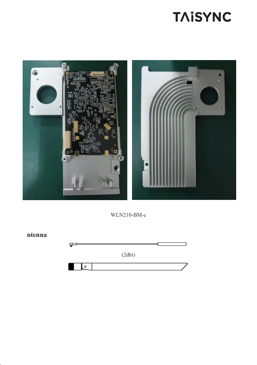
Model:WLN210-BM
40-
Fan interface
Serial port
RF
Antenna
RF
WLN210-BM-c
(2dbi)
(5dbi)
Note: We provide different shielding structures according to different environment, so the
WLN210-BM series contains three different types of structures currently. We number it
WLN210-BM-a/b/c,there are supplementary pictures in the back.
3
Page 4
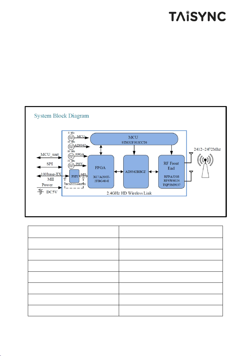
2. Hardware Description
Taisync RF Transmission board is Software Defined Radio Architecture. The system is able to
integrate the latest advanced communication technologies, like orthogonal frequency division
multiplex (OFDM) modulation, Multiple Input Multiple Output (MIMO), low density parity
check (LDPC)code, etc. and has the ability to keep evolving to accommodate future applications.
2.1.System block diagram
Parameters Specifications
Radio Frequency 2.4GHz
Bandwidth 10Mhz, 20MHz
Max. Transmission Power 27dbm(FCC), 20dbm(CE)
LOS Range >12km(27dbm)
Modulation OFDM
FEC LDPC
Duplex TDD
4
Page 5
Data Input Ethernet MII (or 100Base-TX)
RF interface MMCX
Dimensions (mm) 75mmX45mm
Power Input 5.0V/1.5A
Max. Power Consumption 5.5W
2.2.Connecter
Pin definition on 40-Pin connector
Part number: DF12B-40Ds-0p5V_86, Manufacture: HRS
Pin Net Level Description
1 FPGA_DONE LVCMOS(3.3V)
2 MCU_UART2_RX LVCMOS(3.3V) UART2
3 FPGA_GPIO1 LVCMOS(3.3V) GPIO
4 MCU_UART2_TX LVCMOS(3.3V) UART2
5 MII_RXC LVCMOS(3.3V) FPGA_MII
6 MII_TXC (ETH_TDP) LVCMOS(3.3V)
7 MII_RXD0 LVCMOS(3.3V)
8 MII_TXEN (ETH_TDN) LVCMOS(3.3V)
9 MII_RXD1 LVCMOS(3.3V)
10 MII_TXD0 (ETH_RDP) LVCMOS(3.3V)
11 MII_RXD2 LVCMOS(3.3V)
12 MII_TXD1 (ETH_RDN) LVCMOS(3.3V)
13 MII_RXD3 LVCMOS(3.3V)
14 MII_TXD2 (ETH_ACTLED) LVCMOS(3.3V)
15 MII_RXDV LVCMOS(3.3V)
16 MII_TXD3(ETH_LNKLED) LVCMOS(3.3V)
5
(or 100BASE-TX)
Page 6

17 SBUS_PPM LVCMOS(3.3V) Remote signal
18 CAN_TX LVCMOS(3.3V) CAN
19 FPGA_GPIO2 LVCMOS(3.3V) GPIO
20 CAN_RX LVCMOS(3.3V) CAN
21 FPGA_GPIO3 LVCMOS(3.3V) GPIO
22 FPGA_SPI_SCK LVCMOS(3.3V) SPI
23 FPGA_GPIO4 LVCMOS(3.3V) GPIO
24 FPGA_SPI_MOSI LVCMOS(3.3V) SPI
25 FPGA_PROG LVCMOS(3.3V)
26 FPGA_SPI_CS LVCMOS(3.3V) SPI
27 MCU_RST LVCMOS(3.3V) MCU_RST
28 FPGA_SPI_MISO LVCMOS(3.3V) SPI
29 FPGA_GPIO5 LVCMOS GPIO
30 GND GROUND POWER
31 GND GROUND
32 GND GROUND
33 GND GROUND
34
VCC_IN(5V)
35
VCC_IN(5V )
36
VCC_IN(5V )
37 GND GROUND
38
VCC_IN(5V )
39 GND GROUND
40
VCC_IN(5V )
2.3.Debug
POWER@0.3A
POWER@0.3A
POWER@0.3A
POWER@0.3A
POWER@0.3A
This is a 12PIN side mount, mainly used for debugging MCU and FPGA, and provides a
debugging serial port. Type: SH-1X12P_1P0MM.
6
Page 7

Pin
1 MCU1_JTMS-SWDIO
2 MCU1_JTCK-SWCLK LVCMOS(3.3V)
3 NRST# MCU_RST LVCMOS(3.3V)
4 GND Ground POWER
5 3.3V Power source POWER
Signal name Signal description
MCU_DEBUG
Level attributes -
LVCMOS(3.3V)
Remarks
6 JTAG_TCK
7 JTAG_TMS LVCMOS(3.3V)
8 JTAG_TDO LVCMOS(3.3V)
9 JTAG_TDI LVCMOS(3.3V)
10 MCU1_USART1_RX
11 MCU1_USART1_TX LVCMOS(3.3V)
12 GND Ground POWER
FPGA_JTAG
debugging serial
port
LVCMOS(3.3V)
LVCMOS(3.3V)
2.4.Interface board
We also provide a test broad that can be used with this wireless module(WLN210-BM).
There are MB_LAN board, MB_HDMI&USB-OUT board, MB_HDMI-IN board,which can
support different external communication interfaces.
Micro USB(upgrade)port
Transmission boards with any interface board provide a microUSB interface.
Lan port
This interface will only be provided with the LAN board.
UART port
Transmission boards with any interface board provide a UART interface.
HDMI port(in & out)
7
Page 8

MB_HDMI&USB-OUT Supports a HDMI video onput interface.
MB_HDMI-IN Supports a HDMI video input interface.
PPM/S.bus port(in & out)
Interface definition and line order: 凸 G V+ G L H(PPM/SBUS, GND, POWER(3.3V), GND,
CAN_L, CAN_H). Can bus is not supported now.
USB port
This port supports connecting mobile phone to output video.
Power port
Power supply port for the whole module.
8
Page 9

3. Other structure
3.1.ETH module (WLN210-BM-a)
9
Page 10

3.2.HDMI-in module (WLN210-BM-b)
10
Page 11

3.3.HDMI -out module(WLN210-BM-c)
4. Unit combination
4.1.Air unit
Air unit(video input with HDMI port): transmission board, MB_HDMI-IN board.
Air unit(video input with LAN port): transmission board, MB_LAN board.
4.2.Ground unit
Ground unit(video output with HDMI&USB port): transmission board, MB_HDMI&USB-OUT
board.
Ground unit(video output with LAN port): transmission board, MB_LAN board.
11
Page 12

4.3.System setup
Any combination of the air unit and the ground unit can setup communication.
Choose different combinations according to different application scenarios.
5. Software Program
5.1.Transmission board
Tranmission board needs to program baseband and MCU1 firmware.
Tranmission board can be programed for air unit or ground unit.
5.2.Interface board
MB_LAN board can be programed for air unit or ground unit.
MB_HDMI-IN board can only be programed for air unit.
MB_HDMI&USB-OUT board can only be programed for ground unit.
Federal Communications Commission (FCC) Interference
Statement
This equipment has been tested and found to comply with the limits for a
Class B digital device, pursuant to Part 15 of the FCC Rules.
These limits are designed to provide reasonable protection against harmful
interference in a residential installation. This equipment generate, uses and
can radiate radio frequency energy and, if not installed and used in
accordance with the instructions, may cause harmful interference to radio
communications.
12
Page 13

However, there is no guarantee that interference will not occur in a
particular installation. If this equipment does cause harmful interference to
radio or television reception, which can be determined by turning the
equipment off and on, the user is encouraged to try to correct the
interference by one of the following measures:
Reorient or relocate the receiving antenna.
Increase the separation between the equipment and receiver.
Connect the equipment into an outlet on a circuit different from that
to which the receiver is connected.
Consult the dealer or an experienced radio/TV technician for help.
This device complies with Part 15 of the FCC Rules. Operation is subject to
the following two conditions:
(1) This device may not cause harmful interference, and (2) this device
must accept any interference received, including interference that may
cause undesired operation.
FCC Caution: Any changes or modifications not expressly approved by the
party responsible for compliance could void the user’s authority to operate
this equipment.
RF exposure warning
This equipment complies with FCC radiation exposure limits set forth for an
uncontrolled environment. This equipment must be installed and operated
in accordance with provided instructions and the antenna(s) used for this
transmitter must be installed to provide a separation distance of at least 20
cm from all persons and must not be collocated or operating in conjunction
with any other antenna or transmitter.
13
Page 14

OEM Integration Instructions:
This device is intended only for OEM integrators under the following
conditions:
The module can be used to installation in other host. The antenna must be
installed such that 20 cm is maintained between the antenna and users,
and the transmitter module may not be co-located with any other transmit
or antenna. The module shall be only used with the integral antenna(s)
that has been originally tested and certified with this module. As long as 3
conditions above are met, further transmitter test will not be required.
However, the OEM integrator is still responsible for testing their end-
product for any additional compliance requirement with this module
installed (for example, digital device emission, PC peripheral requirements,
etc.)
IMPORTANT NOTE:
In the event that these conditions cannot be met (for example certain
laptop configuration or co-location with another transmitter), then the FCC
authorization for this module in combination with the host equipment is no
longer considered valid and the FCC ID of the module cannot be used on
the final product. In these and circumstance, the OEM integrator will be
responsible for re-evaluating. The end product (including the transmitter)
and obtaining a separate FCC authorization. The final end product must
be labeled in a visible area with the following: “Contains Transmitter
Module FCC ID: 2AQVB-T19V0315 or Contains FCC ID: 2AQVB-
T19V0315”.
14
Page 15

Antenna Specification:
Antenna Name Frequency
Band
TX Paths Max Peak Gain
(dBi)
(GHz)
RP-SMA Antenna
(Ant 1)
PCB Antenna
(Ant 2)
2.4 ~ 2.5 1 5.0
2.4 ~ 2.5 1 2.0
Note: The device can only use the Ant 1 When it is working at 2.5MHz
Bandwidth.
15
 Loading...