

Page 1

LCD Television
Service Manual
Chassis:
Product:
9206B
LTDN40D50TAM
LHD32D50TAM
Ver 1.0
Hisense Electric Co.,Ltd.
May , 2015
Page 2

Content
Content ................................................................................................................................................................... - 2 -
Service Manual ...................................................................................................................................................... - 3 -
1. Precautions and notices ................................................................................................................................ - 3 -
1.1 Warning .............................................................................................................................................. - 4 -
1.2 Notes .................................................................................................................................................. - 7 -
2. Product Specifications ............................................................................................................................... - 10 -
2.1 Main board layout ............................................................................................................................ - 10 -
2.2 The service manual Includes products ............................................................................................. - 11 -
2.3 TV Front and Rear ........................................................................................................................... - 11 -
3. Factory/Service OSD Menu and Adjustment ............................................................................................. - 18 -
3.1 How to enter the Factory OSD Menu .............................................................................................. - 18 -
3.2 Factory OSD Menu .......................................................................................................................... - 18 -
4. Software updating ...................................................................................................................................... - 21 -
4.1 USB upgrade .................................................................................................................................... - 21 -
4.2 SIS Tool upgrade ............................................................................................................................. - 22 -
5.Trouble shooting ......................................................................................................................................... - 27 -
6. Circuit instruction ...................................................................................................................................... - 33 -
Power assign and Main board signal process ........................................................................................ - 33 -
7. Schematic circuit diagram ......................................................................................................................... - 35 -
8. Explode View ............................................................................................................................................. - 35 -
- 2 -
Page 3

Service Manual
1. Precautions and notices
BEFORE SERVICING THE LCD TV, READ THE SAFETY PRECAUTIONS IN
THIS MANUAL.
WHEN REPLACEMENT PARTS ARE REQUIRED, BE SURE TO USE
REPLACEMENT PARTS SPECIFIED BY THE MANUFACTURER.
Proper service and repair is important to the safe, reliable operation of all Hisense
Electric Co., Ltd Equipment. The service procedures recommended by Hisense and
described in this Service Guide are effective methods of performing service operations.
Some of service
operations require the use of tools specially designed for the purpose. The special tools
should be used when and as recommended.
It is important to note that this manual contains various CAUTIONS and NOTICES
which should be carefully read in order to minimize the risk of personal injury to
service personnel. The possibility exists that improper service methods may damage
the equipment. It is also important to understand that these CAUTIONS and
NOTICES ARE NOT EXHAUSTIVE. Hisense could not possibly know, evaluate and
advise the service trade of all conceivable ways in which service might be done or of
the possible hazardous consequences of each way. Consequently, Hisense has not
- 3 -
Page 4

undertaken any such broad evaluation. Accordingly, a serviceman that uses a service
procedure or tools, which are not recommended by Hisense, must first satisfy himself
thoroughly that neither his safety nor the safe of the equipment
will be jeopardized by the service method selected.
Hereafter throughout this manual, Hisense Electric Co., Ltd will be referred to as
Hisense.
1.1 Warning
1.1.1
Critical components having special safety characteristics are identified with a by
the Ref. No. in the parts list. Use of substitute replacement parts, which do not have
the same specified safety characteristics, may create shock, fire, or other hazards.
Under no circumstances should the original design be modified or altered without
written permission from Hisense. Hisense assumes no liability, express or implied,
arising out of any unauthorized modification of design. Serviceman assumes all
liability.
DANGER CAUTION
TO ENSURE THE CONTINUED RELIABILITY OF THIS PRODUCT, USE ONLY
ORIGINAL MANUFACTURER'S REPLACEMENT PARTS, WHICH ARE LISTED WITH
THEIR PART NUMBERS IN THE PARTS LIST SECTION OF THIS SERVICE GUIDE.
1.1.2.
- 4 -
Page 5

All ICs and many other semiconductors are susceptible to electrostatic discharges
(ESD). Careless handling during repair can reduce life drastically. When repairing,
make sure that
you are connected with the same potential as the mass of the set by a wristband with
resistance. Keep components and tools also at this same potential.
1. Never replace modules or other components while the unit is switched on.
2. When making settings, use plastic rather than metal tools. This will prevent
any short circuits and the danger of a circuit becoming unstable.
1.1.3
To prevent electrical shock, do not use this polarized ac plug with an extension cord,
receptacle, or the outlet unless the blades can be fully inserted to prevent blade
exposure.
To prevent electrical shock, match wide blade or plug to wide slot, fully insert.
1.1.4
When replacement parts are required, be sure to use replacement parts specified by the
manufacturer or have the same characteristics as the original part. Unauthorized
substitutions may result in fire, electric shock, or other hazards.
1.1.5
Safety regulations require that after a repair the set must be returned in its original
condition. In particular attention should be paid to the following points.
-Note: The wire trees should be routed correctly and fixed with the mounted
- 5 -
Page 6

cable clamps.
-The insulation of the mains lead should be checked for external damage.
1.1.6
(1) Do not touch Signal and Power Connector while this product operates. Do not
touch EMI ground part and Heat Sink of Film Filter.
(2) Do not supply a voltage higher than that specified to this product. This may
damage the product and may cause a fire.
(3) Do not use this product in locations where the humidity is extremely high, where
it may be splashed with water, or where flammable materials surround it. Do not
install or use the product in a location that does no satisfy the specified
environmental conditions. This may damage the product and may cause a fire.
(4) If a foreign substance (such as water, metal, or liquid) gets inside the panel
module, immediately turn off the power. Continuing to use the product may cause
fire or electric shock.
(5) If the product emits smoke, and abnormal smell, or makes an abnormal sound,
immediately turn off the power. Continuing to use the product, it may cause fire or
electric shock.
(6) Do not disconnect or connect the connector while power to the product is on. It
takes some time for the voltage to drop to a sufficiently low level after the power has
been turned off. Confirm that the voltage has dropped to a safe level before
disconnecting or connecting the connector.
- 6 -
Page 7

(7) Do not pull out or insert the power cable from/to an outlet with wet hands. It may
cause electric shock.
(8) Do not damage or modify the power cable. It may cause fire or electric shock.
(9) If the power cable is damaged, or if the connector is loose, do not use the product:
otherwise, this can lead to fire or electric shock.
(10) If the power connector or the connector of the power cable becomes dirty or
dusty, wipe it with a dry cloth. Otherwise, this can lead to fire.
(11) Use only with the cart, stand, tripod, bracket, or table specified by the
manufacturer, or sold with the apparatus. When a cart is used, use caution when
moving the cart/apparatus combination to avoid injury from tip-over.
1.2 Notes
Notes on Safe Handling of the LCD panel and during service
The work procedures shown with the Note indication are important for ensuring the
safety of the product and the servicing work. Be sure to follow these instructions.
• Before starting the work, secure a sufficient working space.
• At all times other than when adjusting and checking the product, be sure to turn OFF
the POWER Button and disconnect the power cable from the power source of the TV
during servicing.
• To prevent electric shock and breakage of PC board, start the servicing work at least
30 seconds after the main power has been turned off. Especially when installing and
- 7 -
Page 8

removing
the power board, start servicing at least 2 minutes after the main power has been
turned off.
• While the main power is on, do not touch any parts or circuits other than the ones
specified.
If any connection other than the one specified is made between the measuring
equipment and the high voltage power supply block, it can result in electric shock or
activation of the leakage-detection circuit breaker.
• When installing the LCD module in, and removing it from the packing carton, be
sure to have at least two persons perform the work.
• When the surface of the panel comes into contact with the cushioning materials, be
sure to confirm that there is no foreign matter on top of the cushioning materials
before the surface of the panel comes into contact with the cushioning materials.
Failure to observe this precaution may result in, the surface of the panel being
scratched by foreign matter.
• When handling the circuit board, be sure to remove static electricity from your body
before handling the circuit board.
• Be sure to handle the circuit board by holding the large parts as the heat sink or
transformer. Failure to observe this precaution may result in the occurrence of an
abnormality in the soldered areas.
• Do not stack the circuit boards. Failure to observe this precaution may result in
- 8 -
Page 9
problems resulting from scratches on the parts, the deformation of parts, and
short-circuits due to residual electric charge.
• Routing of the wires and fixing them in position must be done in accordance with the
original routing and fixing configuration when servicing is completed. All the wires
are routed far away from the areas that become hot (such as the heat sink). These wires
are fixed in position with the wire clamps so that the wires do not move, thereby
ensuring that they are not damaged and their materials do not deteriorate over long
periods of time. Therefore, route the cables and fix the cables to the original position
and states using the wire clamps.
• Perform a safety check when servicing is completed. Verify that the peripherals of
the serviced points have not undergone any deterioration during servicing. Also verify
that the screws, parts and cables removed for servicing purposes have all been
returned to their proper locations in accordance with the original setup.
The lightning flash with arrowhead symbol, within an equilateral
triangle is intended to alert the user to the presence of uninsulated
dangerous voltage within the products enclosure that may be of sufficient magnitude
to constitute a risk of electric shock.
The exclamation point within an equilateral triangle is intended to
alert the user to the presence of important operating and maintenance
(servicing) instructions in the literature accompanying the set.
- 9 -
Page 10
2. Product Specifications
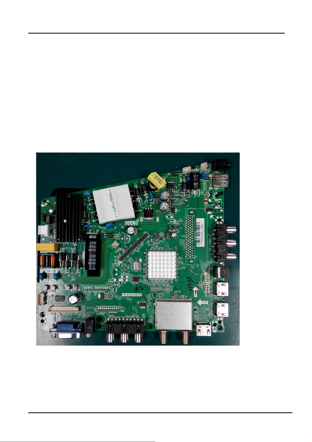
2.1 Main board layout
2.1.1
LTDN40D50TAM use CVTE board:
TP.S512.PB751\40D50TAM\ROH
; 1149238
- 10 -
Page 11
2.2 The service manual Includes products
Product Main & power board(one board) Digital system Panel LVDS cable
LTDN40D50TAM
TP.S512.PB751\40D50TAM\ROH
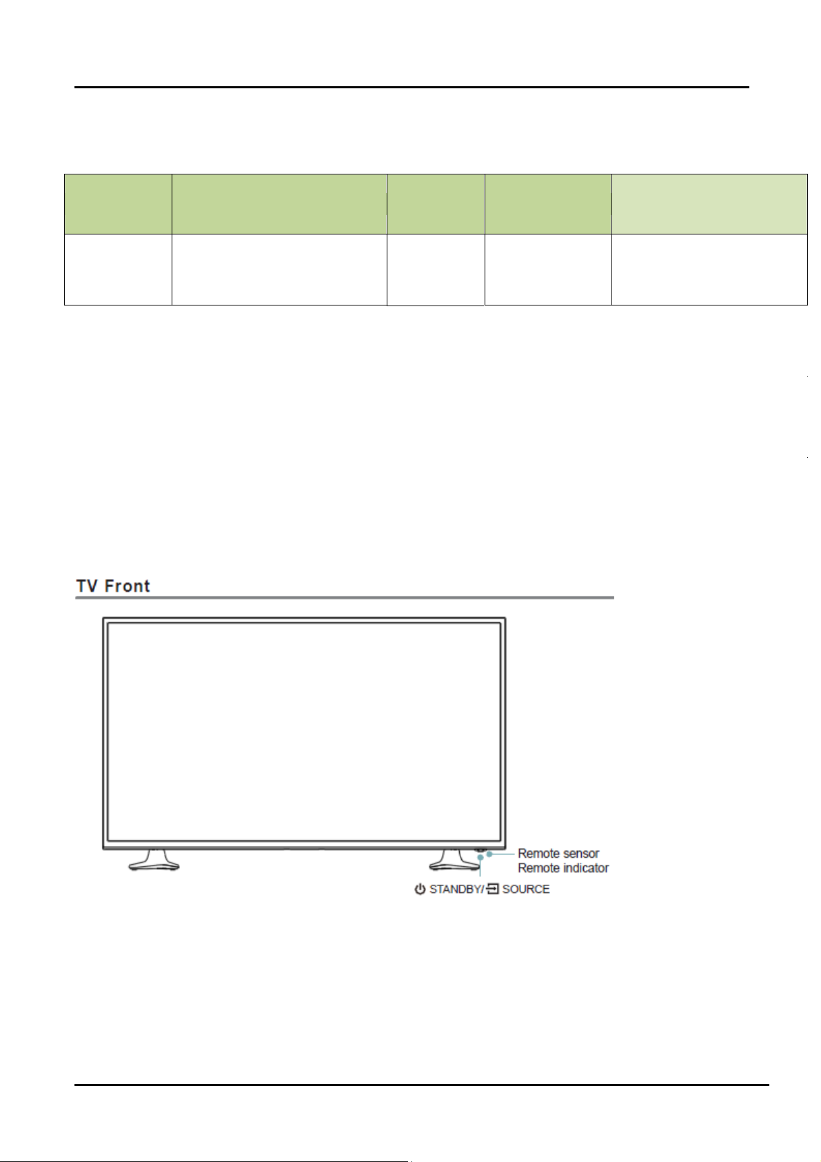
2.3 TV Front and Rear
LTDN40D50TAM TV Front
DVB-T2
JHD396DF-E01
HX2-2X20KLB500P-S-1\500\ROH
- 11 -
Page 12
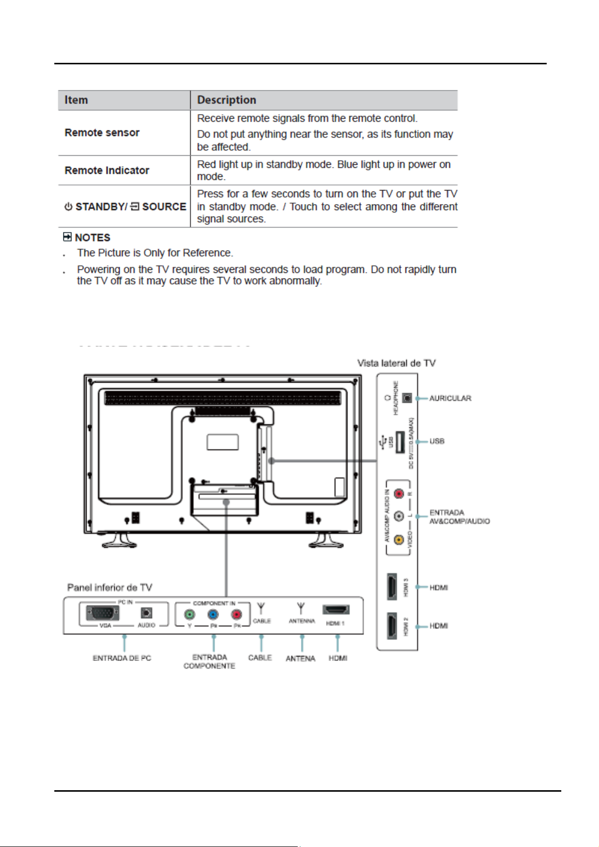
LTDN40D50TAM TV Back
- 12 -
Page 13
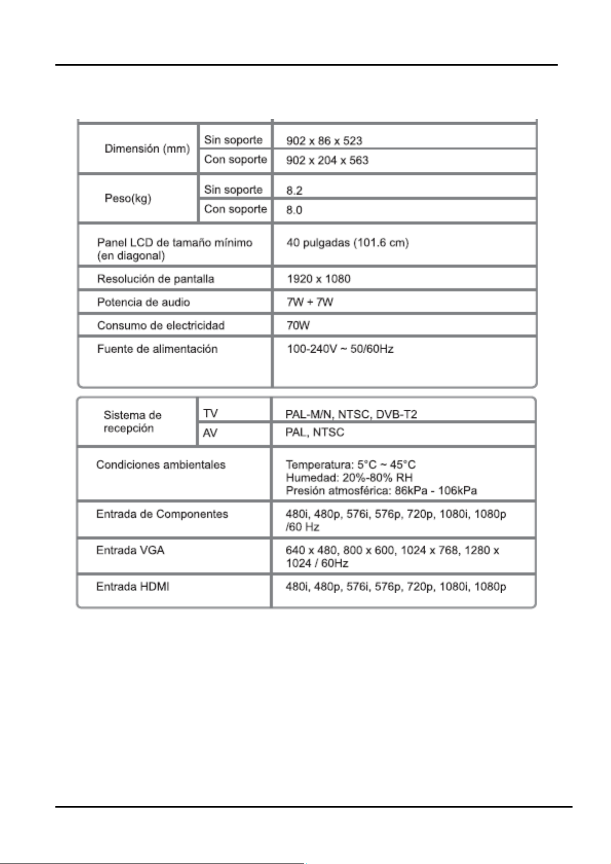
2.4 Specification
- 15 -
Page 14

2.4 Remote control
- 17 -
Page 15

3. Factory/Service OSD Menu and Adjustment
3.1 How to enter the Factory OSD Menu
With user’s RC
Power on the TV.
1. Press “Menu” button and call up User OSD Menu.
2. Select “ Sound” -> press “OK” button on RC to ensure then move button to “Balance”
item.
3. Press number key 1->9->6 ->9 in sequence when “Balance” item is focused.
Note: If necessary, re-do number keys.
4. Factory OSD appears.
Note: DC power off that can exit factory OSD menu.
3.2 Factory OSD Menu
The Factory OSD Menu comprises Factory Menu and Design menu.
3.2.1、Factory Menu
Take LTDN40D50EU for example
White Balance
Input Source
Function
Channel Lint
Test Pattern
Protected clear
Unprotected Clear
Design Menu
- 18 -
Page 16

White Balance:
Colour T emp
R Gain
G Gain
B Gain
R Offset
G Offset
B Offset
Function:
TO Fac M/U
Power mode last memory
Software update start
Uart bebug on/off
Item Default Options Notes
M-Can enter factory mode with
1 MODE M M, U
Note: MODE “M” is only used for factory production.
Init:
Qingdao
Huangdao
Russia
……
U-Can enter factory mode only with
factory RC or user RC.
user’s RC.
- 19 -
Page 17

3.2.2、Design Menu
White balance
Picture Curve
Volu mn Curve
Sound Mode
Note
:
The above “Factory/Service OSD Menus” are reference only, please refer to the actual
unit to determine the appearances.
- 20 -
Page 18

4. Software updating
4.1 USB upgrade
USB upgrade includes two methods. One is USB directly upgrade the other is USB
menu upgrade.
* USB directly upgrade
1、LHD32D50EU upgrading file rename——SIS506_52.bin
LTDN40D50EU upgrading file rename——SIS506_67.bin
2、Unlock the compress upgrading file and copy the SIS506_XX.bin file to the USB
disk root directory which not contain other *.bin files.
3、AC Power off the TV ,insert the USB disk to the Main board USB port then AC power
it on .
Now the TV can update automatically.
4、You can estimate the upgrading state according to the indicator light color
changing.
During upgrading, red indicator and green indicator alternate flicker
slowly ,once/second.
If Upgrading successfully, red indicator and green indicator alternate flicker
fast ,four times/second
If Upgrading failure, red indicator and green indicator alternate flicker,but
flicker time is different. red indicator: 1.75 second/once; green indicator:
250ms/once
* USB menu upgrade
1、Insert USB disk that only have one upgrading file SIS506_XX.bin in root disk.
2、Enter the Factory OSD Menu see 3.1
3、Choose Factory menu->Function>software update >start
When appear “upgrade program detects whether an upgrade”select “YES”to
ensure.
Next:
- 21 -
Page 19

When 100%, next appear:
When 100%, next appear:
It indicates that USB Upgrades successfully.Plug the USB disk ,then TV can automatically restart.
Note:
During upgrading, DO NOT power off the TV and other abnormally
operations .otherwise boot can be destroied .since boot is destroied , USB
upgrading method is availability no longer. Must adopt SIS Tool upgrading.
4.2 SIS Tool upgrade
1、Install Uart driver software for SIS bebug board:CP210x_VCP_Windows
Run CP210xVCPInstaller.exe.
- 22 -
Page 20

2、Hardware connecting
You can update the software through a special tool (as following)
Connect the SIS debug board to TV use VGA port the other USB port to the PC.
USB port Connect
to the PC
Connect to the TV VGA por
3、SIS Tool upgrade with Uart2spi updating Tool
Connect the SIS debug board.
AC power off the TV, unlock compress
Run ,as following.
t
uart2spi_V118.rar
Choose “Comport setting”
- 23 -
Page 21

“Comport setting “item need choose corresponding com port.
How to look up corresponding com port? Now show.as following
- 24 -
Page 22

Click “Connect” button
AC power on the TV, interface as following. click “Restore” item、load the *.bin file then click
“restore “button
- 25 -
Page 23

Updating…… ,about 13 minutes. As following.
after“Restore successful”appears as following.it indicates the main software
upgrading is successful. then AC power off and power on the TV.
- 26 -
Page 24

5.Trouble shooting
5.1 Troubleshooting for Remote Control
Remote control does not work
Try new batteries
NO
Replace RC
Check IR receiver
YES
YES
Replace battery
Replace remote control
Change Led & IR board
NO
Change Led & IR cable
NO
Replace main board
YES
Replace Led & IR BD
YES
Replace Led & IR cable
- 27 -
Page 25

5.2 Troubleshooting for Function Key
Buttons does not work
Check switches
YES
Check solder connections and
see if any switches are stuck.
NO
Check key board
NO
Check Key BD cable
YES
Replace Key BD
YES
Change Key BD
OK
NO
Replace main board
- 28 -
Page 26

5.3 TV won’t Power On
TV won’t power on
Is LED
light?
NO
Check Power
Output
YES
Make Sure Power
source is live
YES
NO
BLUE
RED
Panel Bright
NO
YES
Check signal
Source
YES
NO
Check Power
Cord
NO
Try Power on by
RC and Button
Neither
works
Replace Main
BD
YES
Only
one works
Both
Work
Replace
Power Cord
Check/replace IR
BD or Keypad
PCA
NO
(to contact Hisense tech support.)
Replace Main BD
Replace Panel
OK
YES
Power on
NO
Replace Power BD
YES
OK
Notes:
Above TV configure is that TV in work state, indication Led is blue and in
standby state the indication led is red.
- 29 -
Page 27

5.4 Troubleshooting for Audio
No sound
Check connecter
YES
Reconnect
NO
Check speaker wire
NO
Check speaker set
YES
YES
Replace speaker wire
Replace speaker set
NO
Replace main board
NO
YES
OK
Power Supply Board
- 30 -
Page 28

5.5 Troubleshooting for TV/VGA/HDMI input
No picture on the screen
NO
Check Signal Source
Make sure signal
source is available
YES
Check connect
NO
YES
Check cab l e
NO
Replace main board
Reconnect
Replace cable
- 31 -
Page 29

5.6 Troubleshooting for YPbPr input
Note: (The K220 mould TV has not YPbPr input)
No picture on the screen
Check Source work or not
YES
Check connect
NO
Check Wires (Green Blue, Red)
NO
Replace main board
NO
YES
YES
Check Source Device
Reconnect
Replace wires
- 32 -
Page 30

5.7 Troubleshooting for Video input
No picture on the screen
Check Source work or not
YES
Check connect
NO
Check Cable/ Wires
NO
Replace main board
NO
YES
YES
Check Signal Source
Reconnect
Replace Cable/Wires
6. Circuit instruction
Power assign and Main board signal process
- 33 -
Page 31

- 34 -
Page 32

7. Schematic circuit diagram
8. Explode View
- 35 -
Page 33

1
A A
T3.15AL 250V~
!
!
!
MOVB1
CNB1
!
1
FB1
L
NTCB1
3
N
NC
B B
CXB1
2
! !
!
NC
!
CYB1
RB1
RB2
!
RB3
RB4
CYB2
! !
NC
!
12
43
!
GND
LCB1
!
CYB5
CYB4
3
NC
L
DB1 DB2
GND
DB3 DB4
SGND
Vbridge
!
NC
NC
SGND
RB143靠近IC
4
L
RB141
RB142
RB143
BRO
NC
CB111
放置
UB101
1
GND
2
COMP
BRO
SGND
PCB101B
!
3 4
CB103
NC3CS
RB104
RB103
GATE
5
Vbridge
TP1
+
EB1
TP2
SGND
L
6
5
4
SGND
RB106
RB107
VCC
RB105
CB102
2
113
CB101
RB101
RB102
VCC
NC
RB123
RB118
RB117
DB106
CB114
CB115
AK
D
QB101
G
QB102
RB109
S
RB108
RB110
ZDB1
2
3
RB148
SGND
6
RB124
RB125
RB126
RB127
DB102
11
A K
A K
DB103
CB117
DB101
CB118
+
RB140
GND
RB128
RB129
RB130
+
+
+
EB102
EB101
NC
GND
!
CYB3
CNB2
12V
2
1
GND
!
TB101
6
4
BB101
1
CB116
AK
DB104
DB105
NC
SGND
10
297
RB114
RB115
SGND
CB113
AK
RB111
+
EB106
7
VBL
EB104+EB105
12V
EB103
12V
RB131
12
PCB101A
GNDSGND
!
KA
R
UB102
GND
12V
RB132 RB135
CB109
RB133
CB110
NC
RB134
8
PWM_DIM
PWM_DIM
PWM_DIM
PWM_REF PWM_REF
PWM_REF
C C
GL1
GL2
和散热片之间
QB101
D D
1
EVA1 EVA2 EVA3
NC NC NC NC NC NC NC
MB1
GD1 GD2 GD3
EVA4 EVA5 EVA6 EVA7
ML1
Mylar
2
NC NC NC
HSB1HSHSB2
HS
SGND
HSB3
HSB4
HS
HS
1
2
1
2
1
2
1
2
12V
HS
RB816
12V
3
CB801
GND
4
UB802
1
VIN
2
GATE
GATE
3
GND
GND
COMP
4
PIN4 PIN5
CS
5
PWM_REF
PIN1
UB801
1
VIN
PWM
2
GATE
GATE
OVP
3
GND
COMP
4
CS
FB
PIN4
CB803
CB805
GND
CB812
10
PIN8PIN1
DIM
9
OVP
OVP
8
PIN6
7
FB
REF6ISET
CB811
GATE
GND
RB801
PWM_DIM
PIN8
CB807
8
7
6
5
PIN5
PIN6
RB804
GND
CB806
GND
RB806
RB805
CB804
GND
5
NC
RB803
LED_FB
LB802
6
2 5
VBL
LB801
QB801
RB807
G
RB809
OVP
RB808
NC
DB802
RB818
RB819
RB820
RB821
CB810
RB812
DB801
BB801
RB814
EB801+EB802
OVP
HS
D
S
RB810
GND
NC NC
CB809
6
LED+
+
+
EB803
GND
LED_FB
DB804
GND
AK
RB837
RB838
LED+
NC
RB839
CB808
NC
LED_FB
RB840
RB841
CNB805
CNB803
1
2
123
LED_FB
Model Name:
DRAWN: 林文添
CHK'D:
7
CNB804
CNB801
RB845
2
1
123
LED+
LED_FB
TP.S512.PB751 A14511
CNB806
CNB802
1
2
123
LED+
VERSION:
V1.0
DATE:
2015-01-07
DATE:
2015-01-07
8
Page 34

1
2
3
4
5
6
CD1
RD1
A A
12V
+
CD7
CD8
CD36
ED2
NC/100uF-16V-±20%-5×11-105
GND
NC/10uF-0805-X5R-±20%-16V
10uF-0805-X5R-±20%-16V
1uF-0402-X5R-±20%-16V
100Kohm-0402-±5%-1/16W
RD5
UD1
1
BS
4.5V~18V INPUT
VFB = 0.6V
500KHZ
5
IN
EN4GND
SYH113ADC
℃-黑底白字-编带
LX
-F=2.5-XF
B B
4K7ohm-0402-±5%-1/16W
10Kohm-0402-±5%-1/16WRM8
KMBT3904
1V0_M_EN
POW_EN
10Kohm-0402-±5%-1/16W
KMBT3904
RM7
QM8
GND
0ohm-0402-±5%-1/16W
0.1uF-0402-X5R-±20%-16V
LD1
6
3
FB
2
GND
470uF-10V-±20%-6.3×11-105℃-
RM13
CD3
RD7
5V_STB
RM5
QM4
CD6
CD4
RD3
GND
CTD0504-4R7-M
NC/22pF-0402-NPO-±5%-50V
47Kohm-0402-±1%-1/16W
6K2ohm-0402-±1%-1/16W
GND
NC/10uF-0603-X5R-±20%-6.3V
0.1uF-0402-X5R-±20%-16V
10uF-0805-X5R-±20%-16V
黑底白字-编带
CM4
RM6
4K7ohm-0402-±5%-1/16W
100Kohm-0402-±5%-1/16W
0.1uF-0402-X5R-±20%-16V
WPM2341A-3/TR
0.1uF-0402-X5R-±20%-16V
GND
QM3
5V_STB
CD5
ED1
-F=2.5-XF
CM5
+
+5V
TEST
5V_M
GND
NC/10uF-0805-X5R-±20%-16V
10uF-0805-X5R-±20%-16V
1uF-0402-X5R-±20%-16V
12V
CD13
CD14
CD37
GND
1V0_M_EN
100ohm-0402-±5%-1/16W
0.1uF-0402-X5R-±20%-16V
CD2
RD2
UD2
1
BS
4.5V~18V INPUT
VFB = 0.6V
500KHZ
5
IN
4
EN
SYH112ADC
RD6
CD15
5V_STB 3V3_STB
CD22
LX
FB
GND
UD3
VI3VO
ADJ
6
3
2
GND
2
4
VO
1
GND
0.1uF-0402-X5R-±20%-16V
LC1117CLTR33
GND
0ohm-0402-±5%-1/16W
0.1uF-0402-X5R-±20%-16V
LD2
CD10
CD9
RD4
RD8
GND
CD17
CD16
GND
10uF-0603-X5R-±20%-6.3V
0.1uF-0402-X5R-±20%-16V
+1V
1V0_M
CD12
CD11
GND
CTD0504-4R7-M
NC/22pF-0402-NPO-±5%-50V
4K7ohm-0402-±1%-1/16W
6K04ohm-0402-±1%-1/16W
10uF-0603-X5R-±20%-6.3V
0.1uF-0402-X5R-±20%-16V
10uF-0805-X5R-±20%-16V
TEST
RM3
PANEL_EN
10Kohm-0402-±5%-1/16W
NC/10Kohm-0402-±5%-1/16W
KMBT3904
CD18
NC/10uF-0603-X5R-±20%-6.3V
0.1uF-0402-X5R-±20%-16V
PVCC VCC_PANEL
RM1
CM2
RM2
LED-SHORT
RM4
GND
QM2
GND
5V_STB PVCC
4K7ohm-0402-±5%-1/16W
47Kohm-0402-±5%-1/16W
NC/0.22uF-0402-X5R-±10%-16V
ME2325-G
0.022uF-0402-X7R-±10%-50V
NC/10uF-0805-X5R-±20%-16V
NC/4K7ohm-0402-±5%-1/16W
R5V
NC/0ohm-0805-±5%-1/8W
UD4
2
CD19
VI3VO
CD20
4
ADJ
VO
1
GND GND
GND
LC1117CLTR33
10uF-0603-X5R-±20%-6.3V
0.1uF-0402-X5R-±20%-16V
1uF-0402-X5R-±20%-6.3V
CD21
QM1
D
S
CM3
CM1
RM121
G
GND
R12V
12V PVCCGND
0ohm-0805-±5%-1/8W
3V3_M5V_M
CD49
C C
1V5_DDR5V_M
CD24
CD25
GND
10uF-0603-X5R-±20%-6.3V
10uF-0603-X5R-±20%-6.3V
0.1uF-0402-X5R-±20%-16V
2
BL_ADJ
PWM0
RD14
GND
4K7ohm-0402-±5%-1/16W
4K7ohm-0402-±5%-1/16W
3
RD15
RD10
RD11
CD26
PWM_DIM
PWM_REF
CD27
510ohm-0402-±5%-1/16W
510ohm-0402-±5%-1/16W
47pF-0402-NPO-±5%-50V
1000pF-0402-X7R-±10%-50V
4
5
6
CD29
UD5
VI3VO
2
RD13
CD23
4
VO
ADJ
1
DD1
RD12
CD28
RD16
NC/M7(GOOD-ARK)
0ohm-0402-±5%-1/16W
NC/10uF-0603-X5R-±20%-6.3V
D D
0.1uF-0402-X5R-±20%-16V
GND
LC1117CLTRAD
470ohm-0402-±1%-1/16W
100ohm-0402-±1%-1/16W
GND
1
Page 35

1
CN1
RXP2_A
1
RX2+
2
GND
GND
RXM2_A
3
RX2-
RXP1_A
4
RX1+
5
GND
GND
RXM1_A
6
RX1-
RXP0_A
7
RX0+
GND
8
GND
RXM0_A
9
RX0-
10
RXCP_A
RXC+
GND
11
GND
12
RXCM_A
A A
HD-AF05-S011
HDMI
GND
GND
GND
GND
20
212223
RXC-
13
CEC_A
CEC
14
ARC
ARC
15
CH18 220pF-0402-X7R-±10%-50V
HDMIA_SCL/
SCL
16
HDMIA_SDA/
SDA
GND
17
GND
HDMIA_5V
18
+5V
HOTPLUG_A/
19
HPD
GND
GND
2
5V_STB
RH3
RH4
HDMIA_SCL/
HDMIA_SDA/
CH2
CH3
RH8
GND
HOTPLUG_A/
DH4
CH5
GND
10Kohm-0402-±5%-1/16W
47Kohm-0402-±5%-1/16W
22pF-0402-NPO-±5%-50V
22pF-0402-NPO-±5%-50V
NC/AVLC18S02003
NC/AVLC18S02003
DH1
DH2
CH4
RH31
GND
RH12
3
RH5
RH6
NC/1Mohm-0402-±5%-1/16W
68ohm-0402-±5%-1/16W
68ohm-0402-±5%-1/16W
HDMIA_5V
1000pF-0402-X7R-±10%-50V
NC/AVLC18S02003
NC/10Kohm-0402-±5%-1/16W
0ohm-0402-±5%-1/16W
1000pF-0402-X7R-±10%-50V
HPD_HDMI_A
SCL_HDMI_A
SDA_HDMI_A
4
5
CH1
ARC
0.1uF-0402-X5R-±20%-16V
82ohm-0402-±5%-1/16W
180ohm-0402-±5%-1/16W
RH7
3K3ohm-0402-±5%-1/16W
4K7ohm-0402-±5%-1/16W
6
RH1
HDMI_ARC
RH2
GND
ARC_DETHDMIA_5V
RH9
GND
3V3_STB
RH11
27Kohm-0402-±5%-1/16W
68ohm-0402-±5%-1/16W
DH3
PMLL4148L-F
RH14
CEC_HDMICEC_A
CH6
CH7
100pF-0402-NPO-±5%-50V
NC/1000pF-0402-X7R-±10%-50V
GND
DH5
GND
NC/AVLC18S02003
CN3
RXP2_B
1
RX2+
2
MHL_DET
GND
RXM2_B
3
RX2-
RXP1_B
4
RX1+
5
GND
GND
RXM1_B
6
RX1-
7
RXP0_B
RX0+
8
GND
GND
9
RXM0_B
RX0-
RXCP_B
10
RXC+
GND
11
GND
RXCM_B
12
B B
HD-AF05-S011
HDMI
GND
GND
GND
GND
20
212223
RXC-
13
CEC_A
CEC
14
ARC
HDMIB_SCL/
15
SCL
16
HDMIB_SDA/
SDA
17
GND
GND
18
HDMIB_5V
+5V
HOTPLUG_B/
19
HPD
GND
GND
CH16
HDMIB_5V
UH1
VOUT
VIN
CE
ISET
GND
2
5V_STB
1
RH40
3
RH42
GND
GND
RH38
MHL_DET CD_SENSE
RH39
CH17
NC/33ohm-0402-±5%-1/16W
NC/300Kohm-0402-±5%-1/16W
1000pF-0402-X7R-±10%-50V
NC/10Kohm-0402-±5%-1/16W
GND
NC/100Kohm-0402-±5%-1/16W
GND
MHL_CD_SENSE
5V_STB
CH21
RH43
RH311
GND
5
4
NC/10uF-0603-X5R-±20%-6.3V
NC/4K7ohm-0402-±1%-1/16W
NC/SY6280AAC
NC/10uF-0603-X5R-±20%-6.3V
NC/NC/10Kohm-0402-±5%-1/16W
C C
1716
CN6
NC/WLHD-051A
GND
1
11
R
TXD
NC/100ohm-0402-±5%-1/16W
NC/100ohm-0402-±5%-1/16W
HS_VGA
VS_VGA VSYNC
NC/22pF-0402-NPO-±5%-50V
NC/22pF-0402-NPO-±5%-50V
100ohm-0402-±5%-1/16W
100ohm-0402-±5%-1/16W
SDA_VGA
D D
SCL_VGA
RV18
RV19
RV4
RV6
CV4
CV3
RV7
GND GND
GND
NC/10Kohm-0402-±5%-1/16W
NC/10Kohm-0402-±5%-1/16W
CV9
DV7
DV8
GND
RV8
CV8
DV4
DV3
NC/AVLC18S02003
NC/AVLC18S02003
TXD0/VGA_SDA
RXD0/VGA_SCL
33pF-0402-NPO-±5%-50V
NC/AVLC18S02003
NC/AVLC18S02003
220pF-0402-X7R-±10%-50V
SDA_VGA
HSYNC
SCL_VGA
6
GND
2
12
SDA
G
7
GND
DB15
3
13
HS
B
8
GND
4
14
VS
RXD
9
5V
5
15
SCL
DET
10
GND
GND
GND
CN8
NC/PJ-325
HDMIB_5V
10Kohm-0402-±5%-1/16W
5V_STB
47Kohm-0402-±5%-1/16W
22pF-0402-NPO-±5%-50V
RH15
RH16
22pF-0402-NPO-±5%-50V
NC/AVLC18S02003
HDMIB_SCL/
HDMIB_SDA/
RH23 1Mohm-0402-±5%-1/16W
NC/AVLC18S02003
CH8
CH9
DH6
DH7
68ohm-0402-±5%-1/16W
68ohm-0402-±5%-1/16W
GND
HDMIB_5V
CH12
RH34
GND
HOTPLUG_B/
DH10
RH27
CH14
GND
CV1
RV1
VGA_RIN
NC/AVLC18S02003
NC/NC/10pF-0402-NPO-±5%-50V
NC/75ohm-0402-±5%-1/16W
RV3
NC/AVLC18S02003
NC/75ohm-0402-±5%-1/16W
NC/NC/10pF-0402-NPO-±5%-50V
RV9
RV10
NC/AVLC18S02003
NC/NC/10pF-0402-NPO-±5%-50V
NC/75ohm-0402-±5%-1/16W
NC/330ohm-0402-±1%-1/16W
NC/0.047uF-0402-X7R-±10%-16V
CV2
VGA_GIN
NC/330ohm-0402-±1%-1/16W
NC/0.047uF-0402-X7R-±10%-16V
CV5
VGA_BIN
NC/330ohm-0402-±1%-1/16W
NC/0.047uF-0402-X7R-±10%-16V
DV1
RV2
CV10
GND
DV2
RV5
CV11
GND
DV5
CV12
GND
GND
NC/12Kohm-0402-±5%-1/16W
NC/12Kohm-0402-±5%-1/16W
CV6
CV7
RV13
RV20
NC/12Kohm-0402-±5%-1/16W
NC/12Kohm-0402-±5%-1/16W
1
GND
5
ERO
2
RSPK
3
LSPK
4
ELO
NC/NC/AVLC18S02003
NC/NC/AVLC18S02003
DV6
DV9
GND
RH19
RH21
NC/10Kohm-0402-±5%-1/16W
1000pF-0402-X7R-±10%-50V
NC/AVLC18S02003
1000pF-0402-X7R-±10%-50V
0ohm-0402-±5%-1/16W
HPD_HDMI_B
PC AUDIO_RIN
PC AUDIO_LIN
SCL_HDMI_B
SDA_HDMI_B
CN4
1
RX2+
2
GND
3
RX2-
4
RX1+
5
GND
6
RX1-
7
RX0+
8
GND
9
RX0-
10
RXC+
11
GND
12
RXC-
13
CEC
14
ARC
HDMI
HD-AF05-S011
RXP2_C
RXP1_C RXM1_C
RXP0_C RXM0_C
RXCP_C RXCM_C
HDMIC_SCL/ HDMIC_SDA/
GND GND
HDMIC_5V
GND
CEC_A
,connect jack,2×10Pin,D2.0,D,SNAP,Fool-proofing,Nature,L=2.6mm,DIP,CJ
连接插座
NC/
PC_RIN/
GND
PC/DVD-AR
DVD_RIN/
GND
GND
CN21
3
5 6
7
9
11
13
15
17
1
2
3
4
5
6
GND
GND
GND
20
212223
2
4
8
10
12
14
16
18
20119
UD6
0Y
2Y
Y
3Y
1Y
SW
VEE7A
VSS8B
CD4052
15
SCL
16
SDA
17
GND
18
+5V
19
HPD
RXM2_C
HOTPLUG_C/
GND
VDD
2X
1X
X
0X
3X
GND
RD44
PC AUDIO_RIN
RD45
PC AUDIO_LIN
NC/0ohm-0402-±5%-1/16W
NC/0ohm-0402-±5%-1/16W
CN5
USB-042M-002DP
NC/ULCE0505A015FR
NC/ULCE0505A015FR
USB0_5V
1
5V
USB0_DM
2
DM
USB0_DP
3
DP
4
GND
5
GND
6
GND
GND
NC/100uF-16V-±20%-5×11-105
10uF-0603-X5R-±20%-6.3V
RXP2_C
GND
RXM2_C
RXP1_C
GND
RXM1_C
RXP0_C
GND
RXM0_C
RXCP_C
GND
RXCM_C
CEC_A
HDMIC_SCL/
HDMIC_SDA/
GND
HDMIC_5V
HOTPLUG_C/
RXP2_C
RXP1_C RXM1_C
RXP0_C RXM0_C
RXCP_C RXCM_C
HDMIC_SCL/ HDMIC_SDA/
GND GND
HDMIC_5V
GND
CEC_A
+5V-ASW
16
15
14
GND
13
PC/DVD-AL
PC_LIN/
12
11
DVD_LIN/
10
9
100ohm-0402-±5%-1/16W
PC/DVD-AR
PC/DVD-AL
DU1
DU2
EU1
℃-黑底白字-编带
NC/2*10PIN-2.0-D-H-M
1 2
3 4
5 6
7 8
9 10
11 12
13 14
15 16
17 18
19 20
CN2
RD48
4052-ON/OFF
FU1
MSMD110
+
CU1
-F=2.5-XF
RXM2_C
HOTPLUG_C/
GND
5V_M
CN7
NC/USB-A/F-90°
HDMIC_5V
RH17
HDMIC_SCL/
HDMIC_SDA/
CH10
CH11
RH24
HOTPLUG_C/
DH11
CH15
GND
RD9
5V_M +5V_AUD
330ohm-0402-±5%-1/16W
10uF-0603-X5R-±20%-6.3V
NC/0.1uF-0402-X5R-±20%-16V
NC/200Kohm-0402-±5%-1/16W
CD41
PC AUDIO_RIN PC AUDIO_LIN PC_LIN/
0.1uF-0402-X5R-±20%-16V
200Kohm-0402-±5%-1/16W
CD43
1
USB0_5V
5V-1
USB1_DM
2
DM-1
USB1_DP
3
DP-1
GND
4
GND-1
5
USB0_5V
5V-2
6
USB0_DM
DM-2
7
USB0_DP
DP-2
8
GND
GND-2
NC/ULCE0505A015FR
GND
GND12GND
GND
9
NC/ULCE0505A015FR
101112
GND
10Kohm-0402-±5%-1/16W
5V_STB
47Kohm-0402-±5%-1/16W
RH18
22pF-0402-NPO-±5%-50V
22pF-0402-NPO-±5%-50V
NC/AVLC18S02003
NC/AVLC18S02003
DH8
DH9
1Mohm-0402-±5%-1/16W
68ohm-0402-±5%-1/16W
68ohm-0402-±5%-1/16W
GND
HDMIC_5V
CH13
RH33
GND
RH28
RD34
+5V-ASW
RD36
CD38
GND
+5V_AUD
NC/0.1uF-0402-X5R-±20%-16V
NC/200Kohm-0402-±5%-1/16W
RD35
1Kohm-0402-±5%-1/16W
GND
1Kohm-0402-±5%-1/16W
10uF-0603-X5R-±20%-6.3V
0.1uF-0402-X5R-±20%-16V
PC_RIN/
+5V_AUD
0.1uF-0402-X5R-±20%-16V
RD38
200Kohm-0402-±5%-1/16W
DVD_LINDVD_RIN
DVD_RIN/ DVD_LIN/
DU4
CN91
DU3
GND
RH20
SCL_HDMI_C
RH22
SDA_HDMI_C
HPD_HDMI_C
1000pF-0402-X7R-±10%-50V
NC/10Kohm-0402-±5%-1/16W
0ohm-0402-±5%-1/16W
1000pF-0402-X7R-±10%-50V
NC/AVLC18S02003
CD39
CD40
RD37
CD42
RD39
CD44
CN9
4
4
3
3
2
2
1
1
NC/4PIN-2.0-D-H-G
NC/4PIN-2.0-D-H-G-
USB0_5V
USB1_DM
USB1_DP
GND
-J
带扣
1
2
3
4
5
6
Page 36

1
AV2
PJ-320A(Φ5.5mm)
A A
CN11
NC/RCA-319N-004(
1
GND
2
AV-IN/Y
3
AV-R/Pr
4
AV-L/Pb
4700pF-0402-X7R-±10%-50V
1000pF-0402-X7R-±10%-50V
1
CVBS
2
GND
3
L
4
GND
5
R
6
GND
GND
黄、白、红)-密封
AV_IN/
AV_R
AV_L
AV_IN/
AV_R
AV_L
GND
CI6
CI5
GND
2
RI3
AV_IN/
DI2
CI4
RI4
AVLC18S02003
220pF-0402-X7R-±10%-50V
75ohm-0402-±5%-1/16W
150ohm-0402-±5%-1/16W
0.22uF-0402-X5R-±10%-16V
CI15
AV_R
DI7
CI16
RI23
GND
CI17
AV_L
DI8
CI18
RI24
GND
3
CI3
CVBS1_IN
RI21
AV_RIN
NC/AVLC18S02003
NC/220pF-0402-X7R-±10%-50V
0.1uF-0402-X5R-±20%-16V
12Kohm-0402-±5%-1/16W
12Kohm-0402-±5%-1/16W
RI22
AV_LIN
NC/AVLC18S02003
NC/220pF-0402-X7R-±10%-50V
0.1uF-0402-X5R-±20%-16V
12Kohm-0402-±5%-1/16W
12Kohm-0402-±5%-1/16W
4
NC/AVLC18S02003
180ohm-0402-±5%-1/16W
NC/100ohm-0402-±5%-1/16W
NC/0.1uF-0402-X5R-±20%-16V
NC/330pF-0402-X7R-±10%-50VGND
RI1
SPDIFO COAXSPDIF_OUT
DI1
RI2
GND
5V_M
RI5
SPDIF_OUT
COAX
0ohm-0402-±5%-1/16W
5
AV3
GQ-03-08C
IR Transmitter
Vin
Vcc
GND
GND
GND
CI2
AV1
COAX
1
2
GND
NC/AV19-01S-0020(橙)-
CI1
1
2
3
4
5
6
密封
GND
YPbPr_Y
DI3
RI6
CI19
AVLC18S02003
56pF-0402-NPO-±5%-50V
75ohm-0402-±5%-1/16W
AV5
B B
PJ-320A(Φ5.5mm)
GND
1
GND
2
YPbPr_Y
AV-IN/Y
3
YPbPr_Pr
AV-R/Pr
YPbPr_Pb
4
AV-L/Pb
YPbPr_Pb
YPbPr_Pr
GND
DI4
RI7
CI20
AVLC18S02003
56pF-0402-NPO-±5%-50V
75ohm-0402-±5%-1/16W
GND
DI5
RI8
CI21
AVLC18S02003
56pF-0402-NPO-±5%-50V
75ohm-0402-±5%-1/16W
RI14
YPbPr_Y
RI15
YPbPr_Pb
RI16
YPbPr_Pr Y_Pr
NC/0ohm-0402-±5%-1/16W
NC/0ohm-0402-±5%-1/16W
NC/0ohm-0402-±5%-1/16W
Y_Y
Y_Pb
Y_Y
Y_Pb
Y_Pr
CI11
RI17
CI12
RI18
CI13
RI19
CI14
RI20
SOY2_IN
Y2_IN
PB2_IN
PR2_IN
330ohm-0402-±5%-1/16W
0.047uF-0402-X7R-±10%-16V
150ohm-0402-±5%-1/16W
0.047uF-0402-X7R-±10%-16V
150ohm-0402-±5%-1/16W
0.047uF-0402-X7R-±10%-16V
150ohm-0402-±5%-1/16W
0.047uF-0402-X7R-±10%-16V
GND
5V_VMUX 2V5_CLAMP
GND
GND
RD25
RD24
CND2
NC/11PIN-2.0-D-H-G
CND21
1
2
3
4
C C
5
6
7
8
9
10
11
DVD_EN
D D
10Kohm-0402-±5%-1/16W
10Kohm-0402-±5%-1/16W
KMBT3904
1
RD23
CD33 NC/100pF-0402-NPO-±5%-50V
GND
1
DVD_Y
2
GND
3
4
DVD_Pr
GND
5
DVD_Pb
6
DVD_L_IN DVD_LIN
7
8
9
10
11
GND
DVD_R_IN
GND
DVD_SPDIFIN
12Kohm-0402-±5%-1/16W
12Kohm-0402-±5%-1/16W
12Kohm-0402-±5%-1/16W
12Kohm-0402-±5%-1/16W
带扣
11PIN-2.0-D-H-G-
CD34
CD35
-J
12V 12V_OFF
RM9
QM6
RM11
RM12
RD31
RD32
GND
S
CM6
RM10
ON/OFF
4K7ohm-0402-±5%-1/16W
100Kohm-0402-±5%-1/16W
0.1uF-0402-X5R-±20%-16V
ME2325-G
0.1uF-0402-X5R-±20%-16V
75ohm-0402-±5%-1/16W
75ohm-0402-±5%-1/16W
75ohm-0402-±5%-1/16W
DVD_SPDIFIN SPDIFIN
GND
QM5
G
GND
2
DI6
D
DVD_RIN
R3
RD321
CM7
GND
12V_OFF
12V_OFF
GND
GND
NC/4PIN-2.0-D-H-
NC/4PIN-2.0-D-H-
RI9
YPbPr_Y
YPbPr_Pb
YPbPr_Pr
RI10
RI11
CI7
GND
CI8
CI9
CI10
0.47uF-0402-Y5V-+80%-20%-10V
0.47uF-0402-Y5V-+80%-20%-10V
0.47uF-0402-Y5V-+80%-20%-10V
NC/AVLC18S02003
NC/22ohm-0402-±5%-1/16W
NC/100Kohm-0402-±5%-1/16W
RI12
RI13
1Kohm-0402-±5%-1/16W
470ohm-0402-±5%-1/16W
0.1uF-0402-X5R-±20%-16V
200Kohm-0402-±5%-1/16W
200Kohm-0402-±5%-1/16W
200Kohm-0402-±5%-1/16W
YPbPr_Y/
YPbPr_Pb/
YPbPr_Pr/
MUX_VSW1
YPbPr_Pb/
DVD_Pb
Y_Pb
YPbPr_Y/
DVD_Y
Y_Y
GND
UC1
SGM330A-YQS/TR-(C)
1
S
2
I0A
3
I1A
4
YA
5
I0B
6
I1B
7
YB
8
GND
控制逻辑
YPbPr
DVD01
5V_M 5V_VMUX
16
VCC
15
E
14
I0D
13
I1D
12
YD
11
I0C
10
I1C
9
YC
MUX_VSW1
RC1
GND
GND
GND
GND
YPbPr_Pr/
DVD_Pr
Y_Pr
0.1uF-0402-X5R-±20%-16V
100ohm-0402-±5%-1/16W
CC1
GND
RD26
DVD_Y
RD27
DVD_Pb
RD29
DVD_Pr Y_Pr
NC/0ohm-0402-±5%-1/16W
NC/0ohm-0402-±5%-1/16W
NC/0ohm-0402-±5%-1/16W
Y_Y
Y_Pb
GND
5V_STB
10Kohm-0402-±5%-1/16W
10Kohm-0402-±5%-1/16W
KMBT3904
CN101
DVD5V_EN
CN10
4
4
3
3
2
2
1
1
-G
蓝色
-G-带扣-J
蓝色
RM14
RM16
RM17
3
QM9
GND
CM8
RM15
4K7ohm-0402-±5%-1/16W
100Kohm-0402-±5%-1/16W
0.1uF-0402-X5R-±20%-16V
WPM2341A-3/TR
0.1uF-0402-X5R-±20%-16V
NC/0ohm-0402-±5%-1/16W
4
DVD_5V
QM7
CM9
GND
RM18
ON/OFF
CND11
CND1
DVD_5V
8
8
7
7
DVD_5V
6
GND
6
5
5
GND
12V_OFF
4
4
3
3
2
1
RD20
2
RD21
1
RD22
CD30
CD31
CD32
GND
5
带扣
8PIN-2.0-D-H-G-
-B
NC/8PIN-2.0-D-H-G
3V3_M
RD17
NC/10Kohm-0402-±5%-1/16W
NC/10Kohm-0402-±5%-1/16W
10Kohm-0402-±5%-1/16W
RD19
RD18
100ohm-0402-±5%-1/16W
100ohm-0402-±5%-1/16W
100ohm-0402-±5%-1/16W
NC/0.1uF-0402-X5R-±20%-16V
NC/0.1uF-0402-X5R-±20%-16V
NC/0.1uF-0402-X5R-±20%-16V
DVD_IR
DVD_DAT
DVD_STB
6
Page 37

1
2
3
4
5
6
A A
FCM1005KF-121T06(120ohm-500mA)
10uF-0603-X5R-±20%-6.3V
0.1uF-0402-X5R-±20%-16V
CI_IOWR
CI_IORD
0ohm-0402-±5%-1/16W
0ohm-0402-±5%-1/16W
NC/10pF-0402-NPO-±5%-50V
B B
LC1
RC14
RC12
0ohm-0402-±5%-1/16W
0ohm-0402-±5%-1/16W
V_5V_CI5V_M
CC7
CC6
GND
RC10
CI_OE
CC5
RC11
CI_WE
GND
GND
AV13
51
VCC
17
VCC
30
CI_D0
D0
31
CI_D1
D1
32
CI_D2
D2
2
CI_D3
D3
3
CI_D4
D4
4
CI_D5
D5
5
CI_D6
D6
6
CI_D7
D7
CI_WAIT
WAIT#59INPACK#
16
CI_IRQ
IRQ#
58
CI_RST
RESET
45
PC_IOW
IOWR#
44
PC_IOR
IORD#
9
ROM_OE
OE#
15
FLASH_WE TSO_VAL
WE#
61
CI_REG_N
REG#
14
A14
13
A13
21
A12
10
CI_A11/TSO_D0
A11
8
CI_A10/TSO_D1
A10
11
CI_A9/TSO_D2
A9
12
CI_A8/TSO_D3
A8
22
CI_A7/TSO_D4
A7
23
CI_A6/TSO_D5
A6
24
CI_A5/TSO_D6
A5
25
CI_A4/TSO_D7
A4
26
CI_A3
A3
27
CI_A2
A2
28
CI_A1
A1
29
CI_A0
A0
34
GND
35
GND
1
GND
68
GND
PC-CL1D-PV-A03-C-03
GND
SCART_VIN CVBS2_IN
CS6
DS2
CN12
SC_ROUT
1
AR-OUT
SC_RIN
2
AR-IN
SC_LOUT
3
AL-OUT
GND
4
NC/CS-116B-EP-
A-GND
GND
5
B-GND
SC_LIN
6
AL-IN
SCART_Bin
7
B-I/O
8
SCART1_FUNSEL
FSW-I/O
9
GND
G-GND
10
CLK-OUT
11
SCART_Gin
G-I/O
12
DATA
13
GND
R-GND
GND
14
D-GND
SCART
SCART_Rin
15
R-I/O
FSCART_FB
16
BK-I/O
GND
17
V-GND
GND
18
BK-GND
SCART_VOUT
19
V-OUT
SCART_VIN
20
V-IN
21
GND
GND
密封
C C
SC_RIN
SC_LIN
GND
DS4
CI22
GND
DS8
CI23
GND
CN13
CVBS
GND
L
GND
R
GND
黄、白、红)-密封
RCA-319N-004(
D D
SCART_VIN
1
2
SC_LIN
3
4
5
SC_RIN
6
DS10 NC/NC/AVLC18S02003
GND
V_5V_CI
18
VPP1
52
VPP2
RC8 22ohm-0402-±5%-1/16W
7
CI_CE1
CE1#
42
CE2#
67
CD2#
36
CD1#
43
VS1#
33
IOIS16#
60
46
MISTRT
20
MCLKI
19
MIVAL
47
MDI0
48
MDI1
49
MDI2
50
MDI3
53
MDI4
54
MDI5
55
MDI6
56
MDI7
63
MOSTRT
57
RC5 22ohm-0402-±5%-1/16W
MCLKO
62
MOVAL
64
TSI_D0
MDO0
65
TSI_D1
MDO1
66
TSI_D2
MDO2
37
TSI_D3
MDO3
38
TSI_D4
MDO4
39
TSI_D5
MDO5
40
TSI_D6
MDO6
41
TSI_D7
MDO7
69
GND
70
GND
CI_A11/TSO_D0
CI_A10/TSO_D1
CI_A9/TSO_D2
CI_A8/TSO_D3
CI_A7/TSO_D4
CI_A6/TSO_D5
CI_A5/TSO_D6
CI_A4/TSO_D7
CIIN_CD1
TSI_SYNC
TSI_VAL
TSO_SYNC
GND
CI_CE
CC4
GND
RC2
CC2
NC/10pF-0402-NPO-±5%-50V
22ohm-0402-±5%-1/16W
TSI_CLK
1Kohm-0402-±5%-1/16W
CC3
NC/10pF-0402-NPO-±5%-50V
GND
NC/10pF-0402-NPO-±5%-50V
TSO_CLK
GND
SCART_Gin
RS2
SCART1_FUNSEL SCART_FSFSCART_FB SCART_FB
DS1
GND
DS5
GND
SCART_Rin
DS9
GND
RS14
RS19
DS11
GND
CS3
RS4
RS7
0.22uF-0402-X5R-±10%-16V
AVLC18S02003
NC/220pF-0402-X7R-±10%-50V
75ohm-0402-±5%-1/16W
150ohm-0402-±5%-1/16W
CS11
RS11
RI25
AVLC18S02003
1500pF-0402-X7R-±10%-50V
12Kohm-0402-±5%-1/16W
12Kohm-0402-±5%-1/16W
0.1uF-0402-X5R-±20%-16V
RS17
RI26
AVLC18S02003
1500pF-0402-X7R-±10%-50V
12Kohm-0402-±5%-1/16W
12Kohm-0402-±5%-1/16W
0.1uF-0402-X5R-±20%-16V
SC_RIN/
CS13
SC_LIN/
RS23
RS27
CS18
NC/75ohm-0402-±5%-1/16W
NC/220ohm-0402-±5%-1/16W
GND GND
GND
NC/100pF-0402-NPO-±5%-50V
GND
CI_REG_N
RS24
RS28
RC20
CS1
RS1
Y1_IN
NC/AVLC18S02003
NC/75ohm-0402-±5%-1/16W
NC/150ohm-0402-±5%-1/16W
NC/0.047uF-0402-X7R-±10%-16V
CS12
RS12
PB1_INSCART_Bin
NC/AVLC18S02003
NC/75ohm-0402-±5%-1/16W
NC/150ohm-0402-±5%-1/16W
NC/0.047uF-0402-X7R-±10%-16V
CS14
RS18
PR1_IN
NC/AVLC18S02003
NC/75ohm-0402-±5%-1/16W
NC/150ohm-0402-±5%-1/16W
NC/0.047uF-0402-X7R-±10%-16V
RS25
NC/NC/AVLC18S02003
NC/22Kohm-0402-±5%-1/16W
NC/6K8ohm-0402-±5%-1/16W
NC/1Kohm-0402-±5%-1/16W
CN17
NC/RCA-319N-004(
SC_LOUT/
SC_ROUT/ SC_ROUT
NC/330ohm-0402-±5%-1/16W
NC/330ohm-0402-±5%-1/16W
NC/NC/0.01uF-0402-X7R-±10%-16V
NC/NC/0.01uF-0402-X7R-±10%-16V
SCART_VOUT SCART_VOUT/
1
SCART_VIN
CVBS
2
GND
3
SC_LIN
L
4
GND
5
SC_RIN
R
6
GND
NC/0ohm-0402-±5%-1/16W
NC/0ohm-0402-±5%-1/16W
GND
NC/0ohm-0402-±5%-1/16W
黄、白、红)-密封
CS4
RS5
CS7
CS8
GND GND GND
NC/1uF-0402-X5R-±20%-6.3V
NC/1uF-0402-X5R-±20%-6.3V
RS15
DS6
DS7
GND
GND
RS10
SCART_VOUT
RS16
SC_LOUT
RS21
SC_ROUT
RS8
RS9
NC/10ohm-0402-±5%-1/16W
RS33
NC/150ohm-0402-±5%-1/16W
NC/AVLC18S02003
NC/NC/AVLC18S02003
GND
CN18
NC/RCA-319N-002(
CS9
NC/AVLC18S02003
NC/AVLC18S02003
NC/4700pF-0402-X7R-±10%-50V
NC/4700pF-0402-X7R-±10%-50V
CS2
RS3
SCART_Gin
SC_LOUT
CS10
1
SCART_VIN
Y
2
GND
3
Pb
4
GND
5
Pr
6
GND
GND
绿、蓝、红)-密封
RS13
RS20
SC_LIN
RS22
SC_RIN
NC/0ohm-0402-±5%-1/16W
NC/0ohm-0402-±5%-1/16W
NC/0ohm-0402-±5%-1/16W
RS6
RS61
NC/330ohm-0402-±5%-1/16W
NC/0.047uF-0402-X7R-±10%-16V
NC/330ohm-0402-±5%-1/16W
SCART_Gin
SCART_Bin
SCART_Rin
CS5
SOY1_INSCART_VIN
Title
Number RevisionSize
A4
Date: 2015/2/26 Sheet of
1
2
3
4
5
File: C:\Users\..\TV#05_SCART&PCMCIA&KEY.SchDocDrawn By:
6
Page 38

1
3V3_STB
AUXOK
R9
C4
GND GND
1Kohm-0402-±5%-1/16W
NC/1uF-0402-X5R-±20%-10V
NC/10Kohm-0402-±5%-1/16W
AUX_PWROK
R11
A A
Crystal Circuit
C5
GND
HW Trap
Y1
C6
Cload: 16pF
33pF-0402-NPO-±5%-50V
33pF-0402-NPO-±5%-50V
24.576MHz-±30PPM-20PF-HC-49S-SMD
R15
4K7ohm-0402-±5%-1/16W
GND
B B
C C
D D
3V3_STB
R27
SPI_CLK
SPI_CS0_N
FLASH_SPI_DI
C31
GND
1
XTALO
XTALI
U2
1
CS#
2
SO
HOLD#
3
WP#
SCLK
Vss4SI
GD25Q64BSIG
10Kohm-0402-±5%-1/16W
0.1uF-0402-X7R-±10%-16V
0.1uF-0402-X5R-±20%-16V
8
Vcc
7
SPI_CLK
6
5
SPI_DO
BL_ADJ
NC/1uF-0402-X5R-±20%-16V
Close to IC
For ESD
PC/DVD-AL
PC/DVD-AR
4.7uF-0603-X5R-±10%-10V
0.1uF-0402-X5R-±20%-16V
0.1uF-0402-X5R-±20%-16V
3V3_STB
C30
GND
SPDIFIN
C13
RXE2_P
RXE2_N
RXE1_P
RXE1_N
RXE0_P
RXE0_N
RXO4_P
RXO4_N
RXO3_P
RXO3_N
RXOC_P
RXOC_N
RXO2_P
RXO2_N
RXO1_P
RXO1_N
RXO0_P
RXO0_N
SCART_FS
SCART_FB
DVD_DAT
DVD_EN
DVD_IR
DVD_STB
3V3_M
1V0_M
KEYPAD0
KEYPAD1
3V3_STB
XTALI
XTALO
POW_EN
IR_DAT
SPI_DO
SPI_CLK
FLASH_SPI_DI
SPI_CS0_N
R1 330ohm-0402-±5%-1/16W
LED_G_ON
ARC_DET
LED_R/
MUTE_AMP
PWM0
AUX_PWROK
1V0_M
PANEL_EN
CD47
CD48
M_SCL/
M_SDA/
2
5V_ANT_ON/OFF
4052-ON/OFF
MUX_VSW1
SPDIFO
C14
VBG_AU
AV_LIN
AV_RIN
SC_LIN/
SC_RIN/
3V3_M
RF3
RF5
RF6
NC/22pF-0402-NPO-±5%-50V
2
1
LVA_CKP
2
LVA_CKN
3
LVA_TXP3
4
LVA_TXN3
5
LVA_TXP4
6
LVA_TXN4
7
LVB_TXP0
8
LVB_TXN0
9
LVB_TXP1
10
LVB_TXN1
11
LVB_TXP2
12
LVB_TXN2
13
LVB_CKP
14
LVB_CKN
15
LVB_TXP3
16
LVB_TXN3
17
LVB_TXP4
18
LVB_TXN4
19
KEY2
20
KEY3
21
RMIIMDIO/SW0
22
RMIIMDC
23
RMII50MCK
24
RMIIRXER/I2S_SCK
25
RMIIRXD0/DVD_AUTO
26
RMIIRXD1
27
RMIIRXDV/SPDIF_IN
28
RMIITXEN/DVD ONOFF
29
RMIITXD0/DVD_IR
30
RMIITXD1/DVD_STB
31
OVDD3P3
32
IVDD1P0
33
VSS1P5_DDR
34
IVDD1P0
35
KEY0
36
KEY1
37
OVDD3P3_AUX
38
OSCI
39
OSCO
40
PWRSW
41
BL_ON/GPIO30(PM)
42
BL_ADJ/GPIO35(PM)
43
IR
44
SPI_DO
45
SPI_CKO/ENTEST
46
SPI_DI
47
SPI_CSN0
48
AUX_I2CM_SDA1
49
AUX_I2CM_SCL1
50
LRSYNC/SPDIF_IN
51
SPK_MUTE/GPIO6(PM)
52
PWM0/GPIO27(PM)
53
SPDIFO/ENDEBUG
54
AUXOK
55
LCD_EN/GPIO43(PM)
56
IVDD1P0
57
VBG_AU
58
AVSS3P3_AU
59
LINEIN_L3
60
LINEIN_R3
61
LINEIN_L2
62
LINEIN_R2
63
LINEIN_L1
64
LINEIN_R1
RF4
M_SCL
M_SDA
CF1
3V3_M
GND
257
PAD
3V3_M 3V3_M
4K7ohm-0402-±5%-1/16W
4K7ohm-0402-±5%-1/16W
100ohm-0402-±5%-1/16W
100ohm-0402-±5%-1/16W
CF2NC/22pF-0402-NPO-±5%-50V
RXE3_N
RXEC_P
RXEC_N
255
253
256
254
LVA_TXP2
LVA_TXN2
LVA_TXN1
AVDD3P3_LVDS
LVDS
LVDS
Audio Out
Audio In
65
SPK_L
SC_LOUT/
SC_ROUT/
3
360ohm-0402-±1%-1/16W
NC/10Kohm-0402-±5%-1/16W
R10
1V0_M
AVDD3P3_MCPLL
1V5_DDR
R12
1V0_M
RXE4_P
RXE4_N
RXE3_P
251
252
250
LVA_TXP1
LVA_TXN0
EFUSE
DDR_ZQ
241
245
246
239
238
237
243
242
244
247
249
LVA_TXP0
VDD1P5_DDR
240
248
NF_IO7
NF_IO6
CK_MA
DDR_ZQ
IVDD1P0
IVDD1P0
EFUSE_GND
VDDQ1P5_DDR
VDDQ1P5_DDR
NF_DQS/I2S_MCK
AVDD3P3_MCPLL
RGB - CVBS
UARTA_TX/VGA_SDA73UARTA_RX/VGA_SCL74VGA_HS75VGA_VS
AVDD3P3_BGP
SPK_R69SPK_L68LINEOUT_R67LINEOUT_L66AVDD3P3_AU
70
SPK_R
HP_L
3V3_M
AVDD3P3_HSADC
IVDD1P0
VGA_B080VGA_G081VGA_REF82VGA_R083AVDD1P0_HSADC89YPP_SOG2
HP_R
AVDD3P3HP_AU71HP_L
76
78
79
77
72
HS_VGA
VS_VGA
C1
HP_R
RXD0/VGA_SCL
TXD0/VGA_SDA
15pF-0402-NPO-±5%-50V
VGA_REF
VGA_BIN
VGA_GIN
VGA_RIN
GND
SOY1_IN
1V0_M 1V0_M
5V_STB
RV11
RV12
4K7ohm-0402-±5%-1/16W
4K7ohm-0402-±5%-1/16W
TXD0/VGA_SDA
RXD0/VGA_SCL
SDA
SCL
3
TSO_SYNC
230
236
235
234
233
232
231
NF_IO5
NF_IO4
NF_IO3
NF_IO2
NF_IO1
NF_IO0
NF_WPN
S2T512
YPP_SOG184YPP_G185YPP1_REF86YPP_B187YPP_R1
88
91
PB1_IN
PR1_IN
Y1_IN
YPBPR1_GREF
SOY2_IN
YPBPR2_GREF
1V0_M
3V3_M 3V3_M
TSO_CLK
TSO_VAL
CI_D2
CI_D1
CI_A4/TSO_D7
CI_A2
CI_A1
CI_A3
CI_D0
CI_A0
CI_A5/TSO_D6
CI_WAIT
CI_RST
229
228
227
TS_CLK
TS_VALID
TS_FRAME
218
225
226
224
223
222
221
220
219
217
216
CI_DAT2
CI_DAT1
CI_DAT0
CI_ADD0
CI_ADD1
CI_ADD2
CI_ADD3
OVDD3P3
CI_RESET
CI_WAIT_N
CI_ADD4/TS_DAT7
YPP_G292YPP2_REF90YPP_B293YPP_R2
AV_Y196AV_Y295AV_REF97IVDD1P0
AVDD3P3_ATV
ATV_CVBSO99DMVINP_I
DMVINN_I
DMVINN_Q
98
100
101
102
IF_IP
IF_IN
C23
C24
SCART_VOUT/
CVBS2_IN
CVBS1_IN
AV_REF
GND
3V3_M
AVDD1P0_DM
NC/22pF-0402-NPO-±5%-50V
NC/22pF-0402-NPO-±5%-50V
NC/22pF-0402-NPO-±5%-50V
NC/22pF-0402-NPO-±5%-50V
AVDD1P0_DM
104
103
IF_QN
C25
C26
GND
105
IF_QP
AVDD3P3_DM
94
PB2_IN
PR2_IN
Y2_IN
4
TSI_D4
TSI_D5
TSI_D3
CI_A7/TSO_D4
CI_A6/TSO_D5
CI_A8/TSO_D3
CI_WE
CI_A9/TSO_D2
CI_IRQ
CI_IOWR
CI_D6
CI_CE
CI_A10/TSO_D1
CI_A11/TSO_D0
CI_OE
CI_IORD
212
209
215
214
213
211
210
207
206
205
204
203
202
208
CI_OE_N
CI_WE_N
CI_IRQ_N
CI_ADD5/TS_DAT6
CI_ADD6/TS_DAT5
CI_ADD7/TS_DAT4
CI_ADD8/TS_DAT3
CI_DAT6
OVDD3P3
CI_CE1_N
CI_IORD_N
CI_IOWR_N
CI_ADD9/TS_DAT2
CI_ADD10/TS_DAT1
CI_ADD11/TS_DAT0
CI
IF HDMI
I2CM_SCL/GPIO5(PM)
I2CM_SDA/GPIO15(PM)
IFGAIN
AVDD3P3_DM
DMVINP
DMVINN
DMVINP_Q
VBG_DM
AVSS3P3_DM
108
111
107
106
110
109
LIFP
LIFN
VBG_DM
C27
GND
IVDD1P0
T2_FEF/I2S_SD0
RFGAIN/I2S_WS
DISEQ_I/HP_DET
DISEQ_O
OVDD3P3
115
114
113
119
112
116
117
118
M_SCL
M_SDA
HP_DET
D_IFAGC
DISEQC_OUT
1V0_M
3V3_M
CI_D7
201
CI_DAT7
HDMIA_RXCN
120
RXCM_A
CI_D5
CIIN_CD1
CI_D4
198
200
199
CI_DAT5
CI_DAT4
CI
USB HDMI
HDMIA_RXCP
HDMIA_RX0N
121
122
123
RXCP_A
RXM0_A
RXP0_A
CI_D3
197
196
195
194
CI_DAT3
CI_CD1_N
CATS_DAT3
CATS_DAT4
CATS_DAT5
AVDD3P3_HDMI_AUX_T
HDMIA_RX0P
HDMIA_RX1N
HDMIA_RX1P
HDMIA_RX2N
HDMIA_RX2P
124
125
126
127
RXP2_A
RXM2_A
RXM1_A
RXP1_A
AVDD3P3_HDMI
TSI_D6
193
CATS_DAT6
CATS_DAT7
CATS_CLK
CATS_VALID
CATS_FRAME
CATS_DAT0
CATS_DAT1
CATS_DAT2
NF_RBN
NF_REN
NF_WEN
NF_ALE
NF_CLE
NF_CEN1
NF_CEN0
OVDD3P3
IVDD1P0
AVDD3P3_USB
USB_DP1
USB_DM1
USB_DP0
USB_DM0
IVDD1P0
IVDD1P0
VDDQ1P5_DDR
VDDQ1P5_DDR
VDD1P5_DDR
DDR_CMPP
DDR_VREF
IVDD1P0
IVDD1P0
IVDD1P0
IVDD1P0
IVDD_SEL
HDMI_ARC
HDMI_CEC
CD_SENSE
HDMIA_SCL
HDMIA_SDA/5V_DCT
HDMIB_SCL
HDMIB_SDA/5V_DCT
HDMIC_SCL
HDMIC_SDA/5V_DCT
HDMIA_HPD/CBUSA
HDMIB_HPD/CBUSB
HDMIC_HPD
VBUS_EN
AVDD1P0_HDMI
HDMIC_RX2P
HDMIC_RX2N
HDMIC_RX1P
HDMIC_RX1N
HDMIC_RX0P
HDMIC_RX0N
HDMIC_RXCP
HDMIC_RXCN
HDMIB_RX2P
HDMIB_RX2N
HDMIB_RX1P
HDMIB_RX1N
HDMIB_RX0P
HDMIB_RX0N
HDMIB_RXCP
HDMIB_RXCN
AVDD3P3_HDMI
128
4.7uF-0603-X5R-±10%-10V
C28
C32
68ohm-0402-±5%-1/16W
68ohm-0402-±5%-1/16W
R25
GND
R28
GND
YPBPR1_GREF VGA_REF
0.047uF-0402-X7R-±10%-16V
0.047uF-0402-X7R-±10%-16V
4
U1
,IC Main Chip,9206B,32bit,Single-Core,LQFP256,SMD,S2-Tek
主芯片
192
TSI_D7
191
TSI_CLK
190
TSI_VAL
189
TSI_SYNC
188
TSI_D0
187
TSI_D1
186
TSI_D2
185
184
183
182
181
180
179
178
177
176
175
USB1_DP
174
USB1_DM
173
USB0_DP
172
USB0_DM
171
170
169
168
167
166
165
164
163
162
161
160
DVD5V_EN
159
HDMI_ARC
158
CEC_HDMI
157
CD_SENSE
156
SCL_HDMI_A
155
SDA_HDMI_A
154
SCL_HDMI_B
153
SDA_HDMI_B
152
SCL_HDMI_C
151
SDA_HDMI_C
150
149
HPD_HDMI_A
148
HPD_HDMI_B
147
HPD_HDMI_C
MHL_CD_SENSE
146
145
144
143
142
141
140
139
138
137
136
135
134
133
132
131
130
129
RXP2_C
RXM2_C
RXP1_C
RXM1_C
RXP0_C
RXM0_C
RXCP_C
RXCM_C
RXP2_B
RXM2_B
RXP1_B
RXM1_B
RXP0_B
RXM0_B
RXCP_B
RXCM_B
C29
C33
AV_REFYPBPR2_GREF
0.047uF-0402-X7R-±10%-16V
0.22uF-0402-X5R-±10%-16V
5
3V3_M
1V0_M
3V3_M
1V0_M
1V5_DDR
1V0_M
AVDD3P3_HDMI_AUX_T
AVDD1P0_HDMI
R26
R29
68ohm-0402-±5%-1/16W
68ohm-0402-±5%-1/16W
5
6
CN14
VCC_PANEL
VCC_PANEL
GND
RXO0_N
RXO2_N
GND
3V3_M
RXE0_N RXE0_P
RXE2_N
RF1
GND GND
RXEC_N RXEC_P
RXE3_N
GND
CON1/
M_SCL/
RXO4_N
RXE4_N
NC/2×20PIN-2.0-D-H-M(
RXOC_N
RXOC_P
RXEC_N
RXEC_P
,connect jack,2×20Pin/without pin6,D2.0,D,SNAP,Fool-proofing,Nature,L=2.6mm,DIP,CJ
连接插座
VCC_PANEL
VCC_PANEL
GND
RXO0_N
RXO1_N
RXO2_N
GND
RXOC_N
RXO3_N
RXE0_N
RXE1_N
RXE2_N
GND
RXEC_N
RXE3_N
GND
CON1/
M_SCL/
RXO4_N
RXE4_N
5V_STB
RK18
RK19
CK6
14
5V
13
RED
12
GRN
11
IR
10
GND
9
K0/S
8
K1/C+
7
K2/C-
6
K3/V+
5
K4/V-
4
K5/M
3
K6/P
2
K7/N
1
GND
S1
1 2
3 4
IR_DAT
4K7ohm-0402-±5%-1/16W
27pF-0402-NPO-±5%-50V
1Kohm-0402-±5%-1/16W
5V_IR
LED_R
LED_G/B
IR
GND
K0/AD
K1
RK27
K2
RK28
K3
RK29
K4
RK30
K5
RK31
K6/AD
K7
RK32
GND
1K5ohm-0402-±5%-1/16W
4K7ohm-0402-±5%-1/16W
12Kohm-0402-±1%-1/16W
K7
GNDGND
DK1
CNK21
IR
GND
1000pF-0402-X7R-±10%-50V
1000pF-0402-X7R-±10%-50V
1000pF-0402-X7R-±10%-50V
22ohm-0402-±5%-1/16W
1Kohm-0402-±5%-1/16W
CNK2
14
13
12
11
10
9
8
7
6
5
4
3
2
1
NC/14PIN-2.0-D-H-G
14PIN-2.0-D-H-G-带扣-B
AVLC18S02003
1000pF-0402-X7R-±10%-50V
TS071H1-A38F-100(C5)
GND
GND
Title
Number RevisionSize
A4
Date: 2015/2/26 Sheet of
File: C:\Users\..\TV#06_S2T512.SchDoc Drawn By:
VCC_PANEL
1 2
GND
3 4
5
7 8
RXO0_P
9 10
RXO1_PRXO1_N
11 12
RXO2_P
GND
13 14
RXOC_PRXOC_N
15 16
RXO3_PRXO3_N
17 18
19 20
21 22
23 24
25 26
27 28
29 30
31 32
33 34
35 36
37 38
39 40
R14
C7 NC/5pF-0402-NPO-±5%-50V
C8
C9
C10
RXE1_PRXE1_N
RXE2_P
RXE3_P
GND
Display
M_SDA/
RXO4_P
RXE4_P
脚长
=2.6mm)-LK(缺第6PIN)
DisplayPWM_DIM
GND
GND
CN141
2
1
4
3
5
8
7
10
9
12
11
14
13
16
15
18
17
20
19
22
21
24
23
26
25
28
27
30
29
313332
34
353736
38
39 40
1K5ohm-0402-±5%-1/16W
NC/MMBT3904(f≥350MHz)
220ohm-0402-±5%-1/16W
NC/10Kohm-0402-±5%-1/16W
LED_G_ON
LED_R
3V3_M
RF2
NC/100ohm-0402-±5%-1/16W
100ohm-0402-±5%-1/16W
NC/0ohm-0402-±5%-1/16W
NC/5pF-0402-NPO-±5%-50V
NC/5pF-0402-NPO-±5%-50V
NC/5pF-0402-NPO-±5%-50V
VCC_PANEL
GND
RXO0_P
RXO1_P
RXO2_P
GND
RXOC_P
RXO3_P
RXE0_P
RXE1_P
RXE2_P
GND
RXEC_P
RXE3_P
GND
Display
M_SDA/
RXO4_P
RXE4_P
RK21
RK22
5V_M
RK20
GND
1Kohm-0402-±5%-1/16W
1000pF-0402-X7R-±10%-50V
AVLC18S02003
1000pF-0402-X7R-±10%-50V
CK1
CK7
CK8
RK23
RK25
DK3
DK4
KEY0
CK2
KEY1
GND
5V_STB
LED_R/
RK24
CK9
CK10
RK34
4K7ohm-0402-±5%-1/16W
12Kohm-0402-±1%-1/16W
9K1ohm-0402-±5%-1/16W
按键参数值
按键
K0
K1
K2
K3
K4
K5
K6
K7(
保留
)
AVLC18S02003
1Kohm-0402-±5%-1/16W
4K7ohm-0402-±1%-1/16W
4K7ohm-0402-±1%-1/16W
3V3_STB
RK26
GND
GND
RK33
3V3_STB
下拉电阻
/ KohmADC分压 / V
0
1.5
4.7
12
4.7
12
0
1.5
6
LED_G/B
QK2
KEYPAD0
KEYPAD1
0
0.798
1.650
2.371
1.650
2.371
0
0.798
Page 39

1
ADC POWER/GND (1.0V/3.3V)
1V0_M
A A
0.1uF-0402-X5R-±20%-16V
3V3_M
10uF-0603-X5R-±20%-6.3V
0.1uF-0402-X5R-±20%-16V
Pin89
C4310uF-0603-X5R-±20%-6.3V
GND
Pin78 Pin79
C45
GND
C44
C46
2
HDMI POWER/GND (1.0V/3.3V)
R30
0ohm-0402-±5%-1/16W
1uF-0402-X5R-±20%-6.3V
0.1uF-0402-X5R-±20%-16V
IVDD POWER (1.0V)
0.1uF-0402-X5R-±20%-16V
0.1uF-0402-X5R-±20%-16V
1V0_M
3
3V3_M 1V0_M AVDD1P0_HDMIAVDD3P3_HDMI3V3_STB AVDD3P3_HDMI_AUX_T
R31
C36
C35
0ohm-0402-±5%-1/16W
1uF-0402-X5R-±20%-6.3V
0.1uF-0402-X5R-±20%-16V
GND GND
0.1uF-0402-X5R-±20%-16V
0.1uF-0402-X5R-±20%-16V
C52
C51
C48
C50
C38
C37
1uF-0402-X5R-±20%-6.3V
0.1uF-0402-X5R-±20%-16V
0.1uF-0402-X5R-±20%-16V
0.1uF-0402-X5R-±20%-16V
Pin161/162/163/164
C53
4
R32
0ohm-0402-±5%-1/16W
1uF-0402-X5R-±20%-6.3V
0.1uF-0402-X5R-±20%-16V
0.1uF-0402-X5R-±20%-16V
0.1uF-0402-X5R-±20%-16V
Pin170/171Pin119 Pin247Pin98Pin77Pin32/34
C54
C55
GND
Pin145Pin128Pin150
C34
Pin177
C40
C56
Pin242
5
PLL POWER/GND (3.3V)
C57
3V3_M
0ohm-0402-±5%-1/16W
10uF-0603-X5R-±20%-6.3V
0.1uF-0402-X5R-±20%-16V
C58
R33
AVDD3P3_MCPLL
Pin243
C41
GND
6
C42
B B
AUDIO POWER/GND (3.3V)
3V3_M
Pin65
C62
1uF-0402-X5R-±20%-6.3V
1uF-0402-X5R-±20%-6.3V
C C
0.1uF-0402-X5R-±20%-16V
0.1uF-0402-X5R-±20%-16V
3V3_M 3V3_STB
Pin31
Pin118 Pin208Pin178 Pin225
C71
GND GND
0.1uF-0402-X5R-±20%-16V
3.3V
0.1uF-0402-X5R-±20%-16V
0.1uF-0402-X5R-±20%-16V
0.1uF-0402-X5R-±20%-16V
C73
C72
C74
Pin71
C63
GNDGND
Pin37
C75
C79
ATV POWER/GND (3.3V)
3V3_M
D D
0.1uF-0402-X5R-±20%-16V
1
Pin100
C81
GND
2
DDR POWER (1.5V)
1V5_DDR AVDD3P3_DM
10uF-0603-X5R-±20%-6.3V
1uF-0402-X5R-±20%-6.3V
LVDS POWER/GND (3.3V)
0.1uF-0402-X5R-±20%-16V
ALL FB except ADC, CVDD : need Rdc<0.2 , Z=300/100MHz , Idc>500mA
Default part : MCB2012S301H
3V3_M
GND
GND
C64
Pin167/168/169
C65
C66
C67
Pin249Pin245/246
0.1uF-0402-X5R-±20%-16V
C68
0.1uF-0402-X5R-±20%-16V
0.1uF-0402-X5R-±20%-16V
USB POWER/GND (3.3V)
Pin256
C76
GND GND
3
0.1uF-0402-X5R-±20%-16V
4
3V3_M
Pin176
C77
DEMOD POWER/GND (3.3V/1.0V)
3V3_M
5
L1
300ohm-0402-±25%
10uF-0603-X5R-±20%-6.3V
0.1uF-0402-X5R-±20%-16V
L2
300ohm-0402-±25%
10uF-0603-X5R-±20%-6.3V
0.1uF-0402-X5R-±20%-16V
Title
Number RevisionSize
A4
Date: 2015/2/26 Sheet of
File: C:\Users\..\TV#07_S2T512 POWER.SchDocDrawn By:
C59
GND
AVDD1P0_DM1V0_M
C69
GND
Pin108
C60
Pin103
C70
6
Page 40

1
2
3
4
5
6
A A
MUTE_AMP AMP_MUTE/
RA1
RA2
CA1
CA3
12V
+
E1
CA2
4K7ohm-0402-±5%-1/16W
4K7ohm-0402-±5%-1/16W
NC/0.1uF-0402-X5R-±20%-16V
RA3
12VAVCC
10ohm-0402-±5%-1/16W
4
LOUT+
3
100ohm-0402-±5%-1/16W
0.033uF-0402-X7R-±10%-16V
0.033uF-0402-X7R-±10%-16V
B B
100ohm-0402-±5%-1/16W
SPK_L
GND
SPK_R
RA6
GND_JP1
NC
GND_JP2
NC
RA13
0.1uF-0402-X5R-±20%-16V
0.1uF-0402-X5R-±20%-16V
100Kohm-0402-±5%-1/16W
NC/0ohm-0402-±5%-1/16W
0.1uF-0402-X5R-±20%-16V
CA15
CA24
CA10
CA14
RA7
AVCC
RA8
1uF-0402-X5R-±20%-16V
1uF-0402-X5R-±20%-16V
CA23
CA25
CA28
CA29
12V
AMP_MUTE/
CA18
RA11
RA12
RA14
AVCC
UA1
1
SD
FAULT
LINP
LINN
GAIN0
GAIN1
AVCC
AGND
GVDD
PLIMIT
RINN
RINP
NC
PVCCL
PVCCL
OUTPL
PGND
OUTNL
BSNL
BSNR
OUTNR
PGND
OUTPR
BSPR
PVCCR
2
3
4
5
6
7
8
9
10
11
12
13
PBTL14PVCCR
12Kohm-0402-±5%-1/16W
NC/10Kohm-0402-±5%-1/16W
0.1uF-0402-X5R-±20%-16V
0.1uF-0402-X5R-±20%-16V
C C
NC/10Kohm-0402-±5%-1/16W
RT9108NBGCP
12V
CA8
28
27
26
CA11
BSPL
25
24
23
22
CA19
CA20
21
20
19
18
17
CA30
12V
16
CA31
15
0.22uF-0402-X5R-±10%-16V
0.22uF-0402-X5R-±10%-16V
1uF-0402-X5R-±20%-16V
1000pF-0402-X7R-±10%-50V
1uF-0402-X5R-±20%-16V
1000pF-0402-X7R-±10%-50V
CA9
0.22uF-0402-X5R-±10%-16V
0.22uF-0402-X5R-±10%-16V
LBA1
LBA2
+
LBA3
LBA4
+
CA32
SCD54TL-220M
SCD54TL-220M
SCD54TL-220M
SCD54TL-220M
NC/UPZ2012E601-2R0TF(600ohm-2000mA)
NC/UPZ2012E601-2R0TF(600ohm-2000mA)
NC/UPZ2012E601-2R0TF(600ohm-2000mA)
NC/UPZ2012E601-2R0TF(600ohm-2000mA)
+
LA1
LA2
+
LA3
LA4
LOUT-
2
ROUT-
ROUT+
1
NC/4PIN-2.54-D-H-G-B
4PIN-2.54-D-H-G-
CA13
CA12
CA17
CA16
CA22
CA21
CA27
CA26
1uF-0603-X5R-±10%-25V
1uF-0603-X5R-±10%-25V
1uF-0603-X5R-±10%-25V
1uF-0603-X5R-±10%-25V
NC/1000pF-0402-X7R-±10%-50V
NC/1000pF-0402-X7R-±10%-50V
NC/1000pF-0402-X7R-±10%-50V
NC/1000pF-0402-X7R-±10%-50V
10uF-0805-X5R-±20%-16V
NC/0.1uF-0402-X5R-±20%-16V
470uF-16V±20%-10×12-105℃-编带-F=5.0-XL
CN16
CN161
4
3
2
1
-B
带扣
LOUT+
LOUT-
ROUT-
ROUT+
HP_R
HP_L
10uF-0805-X5R-±20%-16V
10uF-0805-X5R-±20%-16V
180ohm-0402-±5%-1/16W
180ohm-0402-±5%-1/16W
CN15
PJ-339
CA4
RA4
CA5
RA5
PH-AROUT
PH-ALOUT
DV10
DV11
CA6
CA7
6800pF-0402-X7R-±10%-50V
6800pF-0402-X7R-±10%-50V
AVLC18S02003
AVLC18S02003
GND
3V3_M
GND
1
GND
6
RIN
4
RSPK
2
PH-AROUT
ERO
PH-ALOUT
3
ELO
5
LSPK
7
LIN
RA10
DV12
GND
RA9
HP_DET
AVLC18S02003
10Kohm-0402-±5%-1/16W
1Kohm-0402-±5%-1/16W
D D
Title
Number RevisionSize
A4
Date: 2015/2/26 Sheet of
1
2
3
4
5
File: C:\Users\..\TV#08_AMP.SchDoc Drawn By:
6
Page 41

1
470pF-0402-X7R-±10%-50V
NC/SDCL1005CR27JTDF(顺络)
BAV99-BR
RF
A A
T1
B B
0ohm-0402-±5%-1/16W
T-14.5×25×9-IEC14.5-LHD(
0ohm-0402-±5%-1/16W
CT5
DT1
1
RT6
1
RF_T2_IN
RF_IN
2
GND
3
GND
4
GND
5
GND
6
GND
7
GND
GND
)
一体
1.2pF-0402-NPO-±0.25pf-50V
SDCL1005C2N7STDFM01
RF_INPUT
2
LT4
3
GNDGND
GND
RT62
2
CT4
LT3
RF
220pF-0402-X7R-±10%-50V
SDCL1005CR18JTDF(180nH-0402±5%-C)
SDCL1005CR18JTDF(180nH-0402±5%-C)
CT6
LT7
GND
T-IF-AGC_R840 RT10
CT22
GND
180pF-0402-NPO-±5%-50V
CT33
LT13
D_IFAGC/
10Kohm-0402-±5%-1/16W
0.1uF-0402-X5R-±20%-16V
3
1Kohm-0402-±25%
1Kohm-0402-±25%
SDCL1005CR18JTDF(180nH-0402±5%-C)
0.1uF-0402-X5R-±20%-16V
GND
LT5
GND
LT6
GND
LT9
CT8
GND
TUNER_SCL
TUNER_SDA
4
3V3_Tun
RT1
3V3_Tun
UT1
R840
GND
25
GND
1
RFIN
2
RFIN2
3
TF1
4
TF2
5
DECT1
6
SCL
CT15
CT14
GND
GNDGND
CT1
CT3
LT1
LT2 SDCL1005CR27JTDF(顺络)
CT2
RF_SW
24
23
22
21
20
19
TFL
TFH
VBG
GPIO
DET2
AVDD
SDA7AVDD
AVDD
VOP
VON
VAGC
VAGC2
XTAL_O
DVSS10CP
DVDD11XTAL_I
8
9
12
0.1uF-0402-X5R-±20%-16V
NC/8pF-0402-NPO-±5%-50V
3V3_Tun
RT5
CT19
NC/8pF-0402-NPO-±5%-50V
16MHz-±20PPM-20PF-HC-49S-SMD-JWT
CT16
1K8ohm-0402-±5%-1/16W
6800pF-0402-X7R-±10%-50V
330pF-0402-NPO-±5%-50V
0.1uF-0402-X5R-±20%-16V
NC/10Kohm-0402-±5%-1/16W
0.1uF-0402-X5R-±20%-16V
SDCL1005C68NJTDF(68nH-0402±5%-C)
0.1uF-0402-X5R-±20%-16V
0.022uF-0402-X7R-±10%-16V
3V3_Tun
CT7
18
GND
17
IFn_R840
IFp_R840
0.1uF-0402-X5R-±20%-16V
16
1000pF-0402-X7R-±10%-50V
T-IF-AGC_R840
220ohm-0402-±5%-1/16W
15
CT9
14
CT10
13
GND
YT1
CT12
GND
RT2
XTAL_I
GND
RT11
CT21
GND
D_IFAGC
1Kohm-0402-±5%-1/16W
0.1uF-0402-X5R-±20%-16V
D_IFAGC/
5
NC/4K7ohm-0402-±5%-1/16W
NC/10Kohm-0402-±5%-1/16W
NC/10Kohm-0402-±5%-1/16W
5V_ANT_ON/OFF
IFp_R840
IFn_R840
0.1uF-0402-X5R-±20%-16V
0.1uF-0402-X5R-±20%-16V
220ohm-0402-±5%-1/16W
220ohm-0402-±5%-1/16W
39pF-0402-NPO-±5%-50V
39pF-0402-NPO-±5%-50V
M_SCL
M_SDA
6
LT8
RF_T2_IN
RD42
FT1
5V_ANT
NC/SDCL1608CR56JTDF
NC/FSMD050
CD50
GND
RD40
RD41
QD2
RD43
NC/0.1uF-0402-X5R-±20%-16V
5V_ANT5V_STB
QD1
CD45
NC/KMBT3904
NC/100Kohm-0402-±5%-1/16W
NC/0.1uF-0402-X5R-±20%-16V
NC/WPM2341A-3/TR
NC/0.1uF-0402-X5R-±20%-16V
CD46
GND
GNDGND
GND
CT18
CT20
LT11
IFp
LT12
IFn
0ohm-0402-±5%-1/16W
0ohm-0402-±5%-1/16W
56pF-0402-NPO-±5%-50V
56pF-0402-NPO-±5%-50V
RT12
RT13
CT11
CT13
LIFP
CT34
LIFN
CT17
0.1uF-0402-X5R-±20%-16V
0.1uF-0402-X5R-±20%-16V
GND
TUNER_SCL
TUNER_SDA
CT23
CT24
GND
W=15mil,Gap=18mil
LNB_PW
CS19
GND GND GND GND GND GND
RZ3
DVB_S2
C C
T3
T-14.5×25×9-F14.5-LHD
F-Connector
1
DVB_S2
RF
2
GND
3
GND
4
GND
5
GND
GND
CS30
47pF-0402-NPO-±5%-50V
SDCL1005C22NJTDF
0ohm-0402-±5%-1/16W
3V3_Tun_S2
LT14
1
GND
GND
GND
Bead:
1k@100M & 400ohm
@400M,300mA& R(dc)<0.8 ohm
2.2uF-0402-X5R-±20%-6.3V
5K6ohm-0402-±5%-1/16W
330pF-0402-NPO-±5%-50V
6800pF-0402-X7R-±10%-50V
T41
1 2
Cable
7
D D
GND
8
GND
9
GND
10
GND
NC/T-34.4×28.8×9.0-F14.5-LHD(
1
双头间距
DVB_S2RF_T2_IN
Air
3
GND
4
GND
5
GND
6
GND
GNDGND
=21.5)
RF_T2_IN
NC/1000pF-0402-X7R-±10%-50V
NC/SDCL1005CR22JTDF(
NC/56pF-0402-NPO-±5%-50V
NC/NC/?
NC/0ohm-0402-±5%-1/16W
NC/BAV99-BR
2
68pF-0402-NPO-±5%-50V
100pF-0402-NPO-±5%-50V
CS20NCCS21NCCS23
CS22
100pF-0402-NPO-±5%-50V
100pF-0402-NPO-±5%-50V
100pF-0402-NPO-±5%-50V
0ohm-0402-±5%-1/16W
RS36
RFIN
2
DT2
BAV99-BR
3
21
1
2
GND
CS34
DET
3
4
CS37
VBAT
5
CS39
VBG
0.1uF-0402-X5R-±20%-16V
0.1uF-0402-X5R-±20%-16V
0.1uF-0402-X5R-±20%-16V
CS40
Close to RT710
GND
CS43
CT31
DVB_S2 RF_NTSC
NC/1000pF-0402-X7R-±10%-50V
NC/SDCL1005CR22JTDF(顺络)
NC/NC/?
NC/56pF-0402-NPO-±5%-50V
NC/BAV99-BR
NC/0ohm-0402-±5%-1/16W
NC/0ohm-0402-±5%-1/16W
NC/0.1uF-0402-X5R-±20%-16V
NC/1000pF-0402-X7R-±10%-50V
NC/100ohm-0402-±5%-1/16W
NC/NC/?
NC/0ohm-0402-±5%-1/16W
NC/
,IC switch,870M,QFN12,SMD,PE42750MLAA-Z,Peregrine
开关芯片
CT40
RF_T2
顺络
)
GND
U3
EPAD
GND
DET
LT
VBAT
VBG
CS42
GND
LT20
CS24
GND
CS25
GND
20
19
GND
RF_IN
RT710
VDD6CP
7
CP
RS38
RT4
LT161
GND GND
CT41
GND
VBAT1
18
CLK_OUT
8
XTAL_I_710
XTAL_I
CT321
470ohm-0402-±5%-1/16W
470ohm-0402-±5%-1/16W
39pF-0402-NPO-±5%-50V
39pF-0402-NPO-±5%-50V
RZ1
RZ2
CS26
CS27
S2_SDA
S2_SCL
16
17
GND
SDA
SCLK
VBAT
15
S2_IP
VOP
14
S2_IN
VON
13
S2_QN
VONQ
S2_QP
12
VOPQ
11
0ohm-0402-±5%-1/16W
NC/0ohm-0402-±5%-1/16W
NC/0ohm-0402-±5%-1/16W
VAGC
XTAL_O9XTAL_I
0ohm-0402-±5%-1/16W
10
VAGCS
XTAL_O_710
YT2
NC/16MHz-±20PPM-20PF-HC-49S-SMD-JWT
0ohm-0402-±5%-1/16W
LT101
CT35
DT3
RT31
RF_SW
LT18
3V3_Tun
CT39
LT19
CT42
DT4
GND
M_SDA
M_SCL
CS28 4.7pF-0402-NPO-±5%-50V
CS29 NC/4.7pF-0402-NPO-±5%-50V
CS31 NC/4.7pF-0402-NPO-±5%-50V
GND
CS32 4.7pF-0402-NPO-±5%-50V
IF_IP
CS33
RZ10
CS35
IF_IN
RZ11
IF_QN
CS36
RZ12
CS38
RZ13
IF_QP
NC/0.1uF-0402-X5R-±20%-16V
0.1uF-0402-X5R-±20%-16V
NC/0.1uF-0402-X5R-±20%-16V
0.1uF-0402-X5R-±20%-16V
VAGCS
GND
GND
CT37
CT38
GND
GND
7
9
8
10
11
12
UT3
RF2
GND
C2
GND
GND
RFC
C1
GND
VCC
GND1RF12GND
EPAD
3
GND
3
Close to RT710
RS37
CS41
0.1uF-0402-X5R-±20%-16V
10Kohm-0402-±5%-1/16W
6
5
4
GND
RT61
D_IFAGC/
RF
4
LZ5
NC/120ohm-1206-±25%
M_SDA
M_SCL
NC/22pF-0402-NPO-±5%-50V
NC/22pF-0402-NPO-±5%-50V
CZ8
NC/0ohm-0402-±5%-1/16W
100uF-16V-±20%-5×11-105
0.22uF-0402-X5R-±10%-16V
CZ9
33ohm-0402-±5%-1/16W
33ohm-0402-±5%-1/16W
NC/4K7ohm-0402-±5%-1/16W
3V3_Tun3V3_STB
LT16
120ohm-1206-±25%
0.1uF-0402-X5R-±20%-16V
12V_OFF
LZ1
CDR810-220-K-CH
1N5819-SMA
S2_LNB_SDA
RZ5
RZ6
S2_LNB_SCL
DISEQC_OUT
-F=2.5-XF
℃-黑底白字-编带
12V_LNB12V 12V_LNB
EZ2
+
GND
GND
DZ1
LZ3
CZ2
18
17
LX
VIN
8
VREG
CZ4
UZ1
RT5006GQW
11
IRQ
9
SDA
12
SCL
5
EXTM
10
ADD
GND
GND
RZ7
19
21
5V_M 3V3_Tun
CT25
CT26
NC/10uF-0603-X5R-±20%-6.3V
0.1uF-0402-X5R-±20%-16V
5
LZ2
EZ1 100uF-25V-±20%-6×7-105℃-XF
GND
7
GND
+
BOOST
VCP
LNB
NC
NC
NC
NC
NC
TCAP
GND
14
UT2
LC1117CLTR33
VI3VO
GND
CZ23
1
2
20
16
DZ3
15
13
6
4
3
CZ10
FCM1005KF-121T06(120ohm-500mA)
FCM1005KF-121T06(120ohm-500mA)
NC/0ohm-0402-±5%-1/16W
2
4
ADJ
VO
1
CZ1
10uF-1206-X5R-±10%-25V
120ohm-1206-±25%
1uF-0603-X5R-±10%-25V
0.1uF-0402-Y5V-+80%-20%-25V
DZ2 1N5819-SMA
CZ3
CZ6
CZ7
1N5819-SMA
0.1uF-0402-Y5V-+80%-20%-25V
0.1uF-0402-Y5V-+80%-20%-25V
120ohm-1206-±25%
0.01uF-0402-X7R-±10%-50V
0.01uF-0402-X7R-±10%-50V
3V_Tun
LT17
CT27
CT28
CT47
10uF-0603-X5R-±20%-6.3V
0.1uF-0402-X5R-±20%-16V
1uF-0402-X5R-±20%-6.3V
1uF-0402-X5R-±20%-6.3V
10uF-0603-X5R-±20%-6.3V
LZ4
LT15
LT10
Title
Number RevisionSize
A4
Date: 2015/2/26 Sheet of
File: C:\Users\..\TV#09_TUNER.SchDoc Drawn By:
6
CZ5
3V3_Tun_S2
CT46
LNB_PW
CT29
Page 42

 Loading...