

Page 1

Liquid Crystal Display Television
Service Manual
Chassis: MST6
Product Type:LCD40V57CA
Ver 1.0
Hisense Electric Co.,Ltd.
May. 2008
Page 2

LCD TV Service Manual
Contents
Contents................................................................................................................................................ .. ... .. ......... - 2 -
Service Manual .............................................................................................................................................. .. ... .- 3 -
1. Precautions and notices........................................................................................................................ .. ... .- 3 -
1.1 WARNING ...................................................................................................................................... - 4 -
1.2 NOTES ...................................................................................................................................... .. ... .- 7 -
2. Product Function Specifications..............................................................................................................- 10 -
2.1 Product Function............................................................................................................................- 10 -
2.2 Specifications.................................................................................................................................- 11 -
3. LCD Panel Spec.............................................................................................................................. .. ... ....- 12 -
3.1 General Description.......................................................................................................................- 12 -
3.2 General Features............................................................................................................................- 13 -
4. Chassis Layout and Overall Wiring Diagrams ........................................................................................- 14 -
4.1 Chassis Layout................................................................................................................. .. ... ......... - 14 -
4.2 Main BD........................................................................................................................................- 15 -
4.3 Power BD ........................................................................................................................ .. ... ......... - 1 6 -
4.4 Term inal Board..............................................................................................................................- 16 -
4.4 Wires and Cables Overall Wiring Diagrams .................................................................................- 17 -
5. Factory/Service OSD Menu and Adjustment........................ .. ............................... ..................................- 19 -
5.1 To enter the Factory OSD Menu....................................................................................................- 19 -
5.2 Factory OSD Menu........................................................................................................................- 19 -
6. Software Upgrading........................................................................................................... ......................- 23 -
6.1 Get ready for upgrading..................................................................................................... ............- 23 -
6.2 Upgrading with the ISP_TOOL4.0.9............................................................................................. - 3 2 -
7. Troubleshooting......................................................................................................................... .. ... ......... - 3 7 -
7.1 Troubleshooting for Remote Control.............................................................................................- 37 -
7.2 Troubleshooting for Function Key......................... .............................. .. ... .............................. ....... - 3 8 -
7.3 TV won’t Power On.......................................................................................................................- 39 -
7.4 Troubleshooting for Audio.............................................................................................................- 40 -
7.5 Troubleshooting for TV/VGA/HDMI input................................. ... .. ... .............................. ............- 41 -
7.6 Troubleshooting for YPbPr input............................................................................................... .. ..- 42 -
7.7 Troubleshooting for Video/S-Video/ SCART input.......................................... .............................- 43 -
8. Explode View and explode BOM List................................................... ... .............................. ... .. ............- 44 -
9. Schematic circuit diagram .......................................................................................................................- 45 -
Hisense Confidential
- 2 -
Page 3

LCD TV Service Manual
Service Manual
1. Precautions and notices
BEFORE SERVICING THE LCD TV, READ THE SAFETY PRECAUTIONS IN
THIS MANUAL.
WHEN REPLACEMENT PARTS ARE REQUIRED, BE SURE TO USE
REPLACEMENT PARTS SPECIFIED BY THE MANUFACTURER.
Proper service and repair is important to the safe, reliable operation of all Hisense
Electric Co., Ltd Equipment. The service procedures recommended by Hisense and
described in this Service Guide are effective methods of performing service
operations. Some of these service operations require the use of tools specially
designed for the purpose. The special tools should be used when and as
recommended.
It is important to note that this manual contains various CAUTIONS and NOTICES
which should be carefully read in order to minimize the risk of personal injury to
service personnel. The possibility exists that improper service methods may damage
the equipment. It is also important to understand that these CAUTIONS and
NOTICES ARE NOT EXHAUSTIVE. Hisense could not possibly know, evaluate
and advise the service trade of all conceivable ways in which service might be done
or of the possible hazardous consequences of each way. Consequently, Hisense has
Hisense Confidential
- 3 -
Page 4

LCD TV Service Manual
not undertaken any such broad evaluation. Accordingly, a serviceman that uses a
service procedure or tools, which are not recommended by Hisense, must first satisfy
himself thoroughly that neither his safety nor the safe of the equipment will be
jeopardized by the service method selected.
Hereafter throughout this manual, Hisense Electric Co., Ltd will be referred to as
Hisense.
1.1 WARNING
1.1.1
Critical components having special safety characteristics are identified with a
by
the Ref. No. in the parts list. Use of substitute replacement parts, which do not have
the same specified safety characteristics, may create shock, fire, or other hazards.
Under no circumstances should the original design be modified or altered without
written permission from Hisense. Hisense assumes no liability, express or implied,
arising out of any unauthorized modification of design. Serviceman assumes all
liability.
DANGERCAUTION CAUTION
TO ENSURE THE CONTINUED RELIABILITY OF THIS PRODUCT, USE ONLY
ORIGINAL MANUFACTURER'S REPLACEMENT PARTS, WHICH ARE LISTED WITH
THEIR PART NUMBERS IN THE PARTS LIST SECTION OF THIS SERVICE GUIDE.
Hisense Confidential
- 4 -
Page 5

1.1.2.
All ICs and many other semiconductors are susceptible to electrostatic discharges
(ESD). Careless handling during repair can reduce life drastically. When repairing,
make sure that you are connected with the same potential as the mass of the set by a
wristband with resistance. Keep components and tools also at this same potential.
1. Never replace modules or other components while the unit is switched on.
2. When making settings, use plastic rather than metal tools. This will prevent
any short circuits and the danger of a circuit becoming unstable.
1.1.3
LCD TV Service Manual
To prevent electrical shock, do not use this polarized ac plug with an extension cord,
receptacle, or the outlet unless the blades can be fully inserted to prevent blade
exposure.
To prevent electrical shock, match wide blade or plug to wide slot, fully insert.
1.1.4
When replacement parts are required, be sure to use replacement parts specified by
the manufacturer or have the same characteristics as the original part. Unauthorized
substitutions may result in fire, electric shock, or other hazards.
1.1.5
Safety regulations require that after a repair the set must be returned in its original
condition. In particular attention should be paid to the following points.
-Note: The wire trees should be routed correctly and fixed with the mounted
Hisense Confidential
- 5 -
Page 6

cable clamps.
-The insulation of the mains lead should be checked for external damage.
1.1.6
(1) Do not touch Signal and Power Connector while this product operates. Do not
touch EMI ground part and Heat Sink of Film Filter.
(2) Do not supply a voltage higher than that specified to this product. This may
damage the product and may cause a fire.
(3) Do not use this product in locations where the humidity is extremely high,
where it may be splashed with water, or where flammable materials surround it. Do
LCD TV Service Manual
not install or use the product in a location that does no satisfy the specified
environmental conditions. This may damage the product and may cause a fire.
(4) If a foreign substance (such as water, metal, or liquid) gets inside the panel
module, immediately turn off the power. Continuing to use the product may cause
fire or electric shock.
(5) If the product emits smoke, and abnormal smell, or makes an abnormal sound,
immediately turn off the power. Continuing to use the product, it may cause fire or
electric shock.
(6) Do not disconnect or connect the connector while power to the product is on. It
takes some time for the voltage to drop to a sufficiently low level after the power
has been turned off. Confirm that the voltage has dropped to a safe level before
disconnecting or connecting the connector.
Hisense Confidential
- 6 -
Page 7

(7) Do not pull out or insert the power cable from/to an outlet with wet hands. It
may cause electric shock.
(8) Do not damage or modify the power cable. It may cause fire or electric shock.
(9) If the power cable is damaged, or if the connector is loose, do not use the
product: otherwise, this can lead to fire or electric shock.
(10) If the power connector or the connector of the power cable becomes dirty or
dusty, wipe it with a dry cloth. Otherwise, this can lead to fire.
(11) Use only with the cart, stand, tripod, bracket, or table specified by the
manufacturer, or sold with the apparatus. When a cart is used, use caution when
LCD TV Service Manual
moving the cart/apparatus combination to avoid injury from tip-over.
1.2 NOTES
Notes on Safe Handling of the LCD panel and during service
The work procedures shown with the Note indication are important for ensuring the
safety of the product and the servicing work. Be sure to follow these instructions.
• Before starting the work, secure a sufficient working space.
• At all times other than when adjusting and checking the product, be sure to turn
OFF the POWER Button and disconnect the power cable from the power source of
the TV during servicing.
• To prevent electric shock and breakage of PC board, start the servicing work at least
30 seconds after the main power has been turned off. Especially when installing and
removing the power board, start servicing at least 2 minutes after the main power has
Hisense Confidential
- 7 -
Page 8

been turned off.
• While the main power is on, do not touch any parts or circuits other than the ones
specified. If any connection other than the one specified is made between the
measuring equipment and the high voltage power supply block, it can result in
electric shock or activation of the leakage-detection circuit breaker.
• When installing the LCD module in, and removing it from the packing carton, be
sure to have at least two persons perform the work.
• When the surface of the panel comes into contact with the cushioning materials, be
sure to confirm that there is no foreign matter on top of the cushioning materials
LCD TV Service Manual
before the surface of the panel comes into contact with the cushioning materials.
Failure to observe this precaution may result in, the surface of the panel being
scratched by foreign matter.
• When handling the circuit board, be sure to remove static electricity from your body
before handling the circuit board.
• Be sure to handle the circuit board by holding the large parts as the heat sink or
transformer. Failure to observe this precaution may result in the occurrence of an
abnormality in the soldered areas.
• Do not stack the circuit boards. Failure to observe this precaution may result in
problems resulting from scratches on the parts, the deformation of parts, and
short-circuits due to residual electric charge.
• Routing of the wires and fixing them in position must be done in accordance with
Hisense Confidential
- 8 -
Page 9

the original routing and fixing configuration when servicing is completed. All the
wires are routed far away from the areas that become hot (such as the heat sink).
These wires are fixed in position with the wire clamps so that the wires do not move,
thereby ensuring that they are not damaged and their materials do not deteriorate over
long periods of time. Therefore, route the cables and fix the cables to the original
position and states using the wire clamps.
• Perform a safety check when servicing is completed. Verify that the peripherals of
the serviced points have not undergone any deterioration during servicing. Also
verify that the screws, parts and cables removed for servicing purposes have all been
LCD TV Service Manual
returned to their proper locations in accordance with the original setup.
The lightning flash with arrowhead symbol, within an equilateral
triangle is intended to alert the user to the presence of uninsulated
dangerous voltage within the products enclosure that may be of sufficient magnitude
to constitute a risk of electric shock.
The exclamation point within an equilateral triangle is intended to
alert the user to the presence of important operating and maintenance
(servicing) instructions in the literature accompanying the set.
Hisense Confidential
- 9 -
Page 10
LCD TV Service Manual
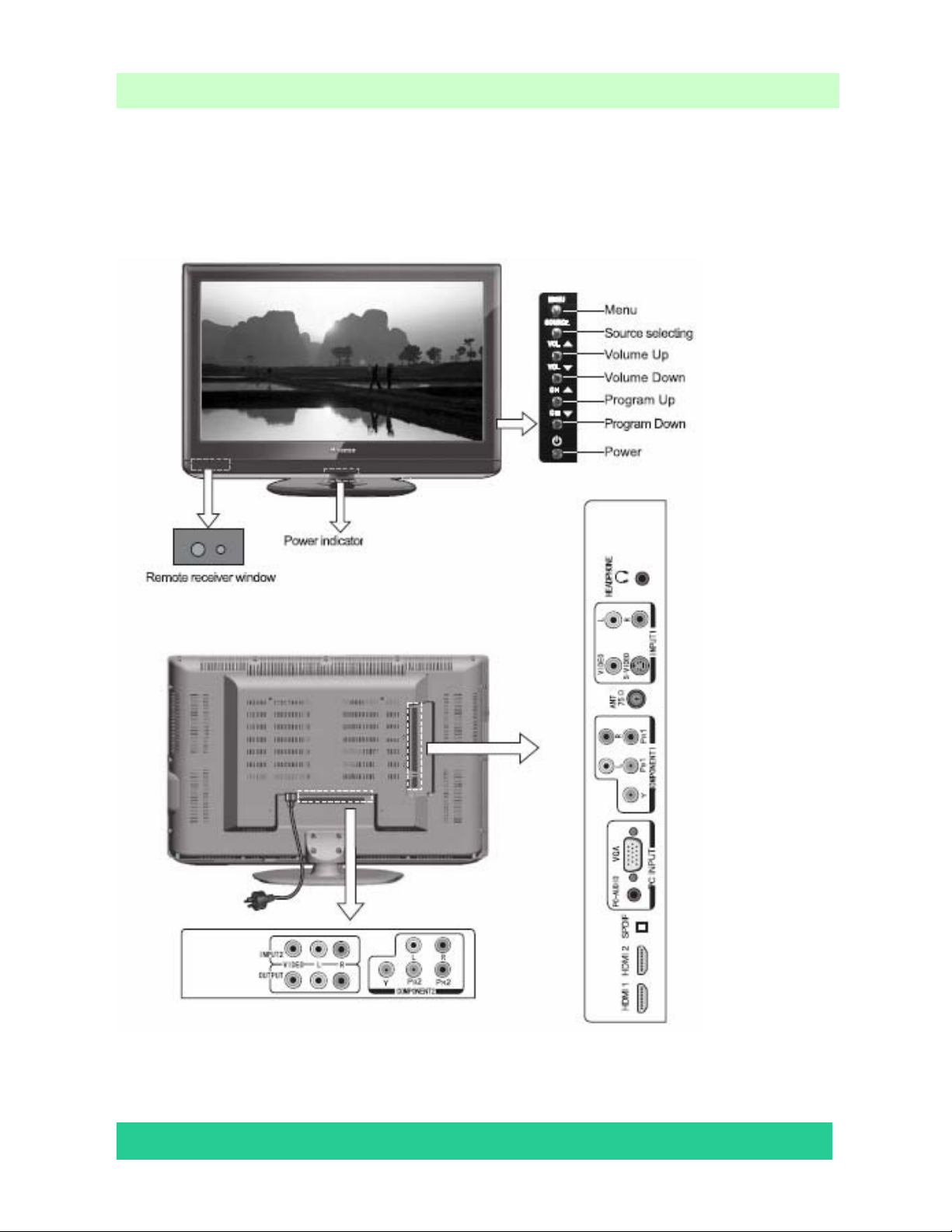
2. Product Function Specifications
2.1 Product Function
Note: The above figures are reference only, please refer to the actual units to determine the
appearances.
Hisense Confidential
- 10 -
Page 11
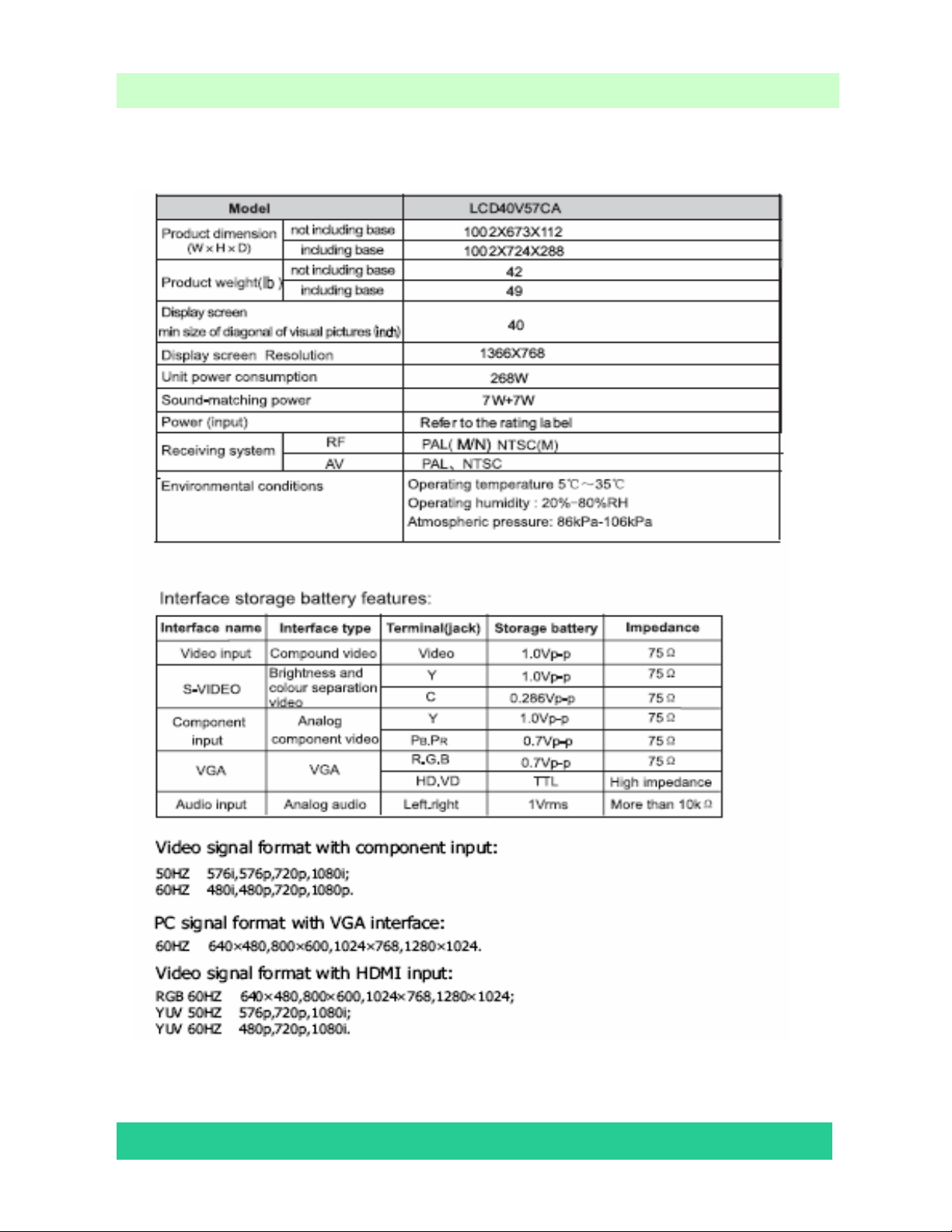
2.2 Specifications
LCD TV Service Manual
Hisense Confidential
- 11 -
Page 12
LCD TV Service Manual
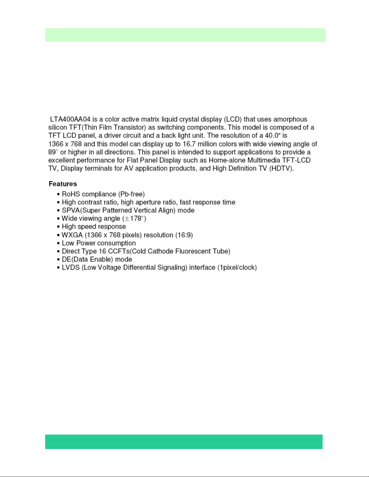
3. LCD Panel Spec
3.1 General Description
SN:1050558
Hisense Confidential
- 12 -
Page 13
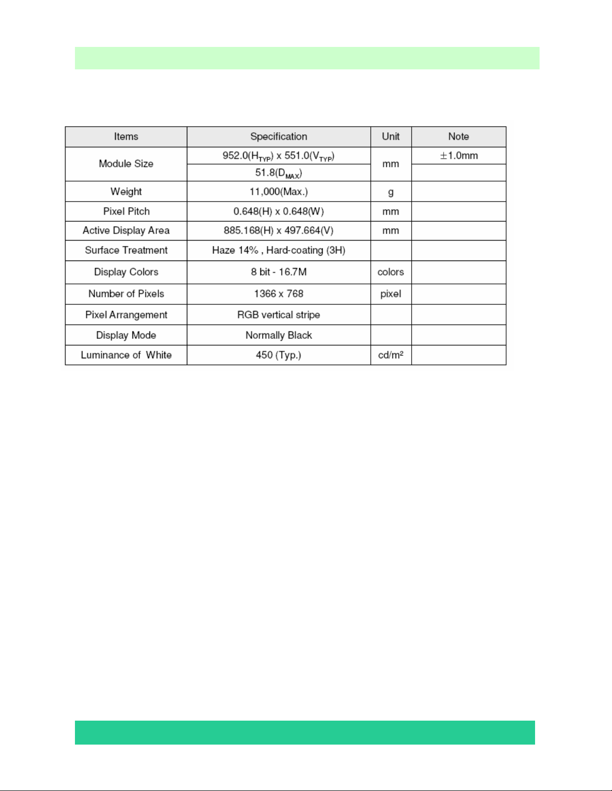
3.2 General Features
LCD TV Service Manual
Hisense Confidential
- 13 -
Page 14
(5)
LCD TV Service Manual
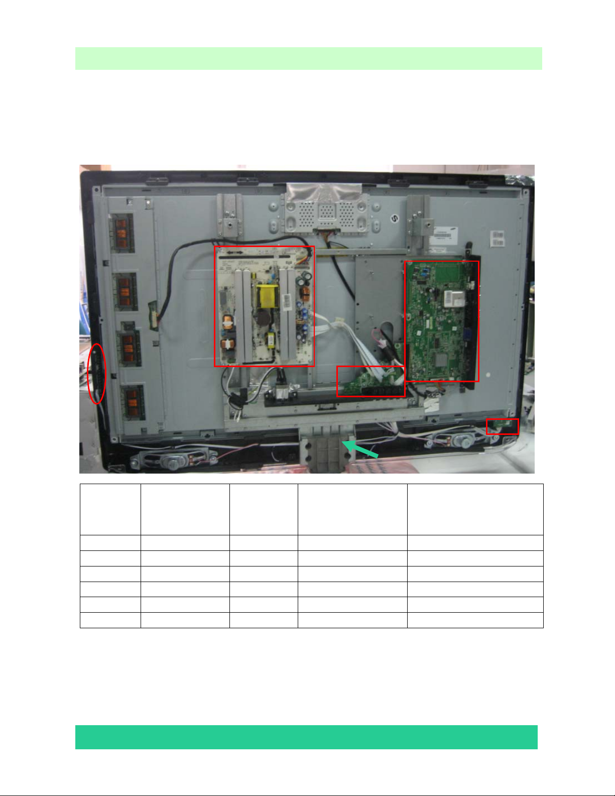
4. Chassis Layout and Overall Wiring Diagrams
4.1 Chassis Layout
(2)
(1)
(4
No Description Part No
(1) Main BD
(2) Power BD
(3) Terminal BD
(4) Keypad PCA
(5) IR Board
(6) luminophor
(3)
(6)
Type/Model PCB/ Model
116622 RSAG2.908.1102-15/ROH
113358 RSAG2.908.982-4/ROH
116706 RSAG2.908.1153-3
113354 RSAG2.908.1088/ROH
112613 RSAG2.908.1029/ROH
1046574 B-700-500
RSAG7.820.1138VER.D/ROH
RSAG7.820.968VER.H/ROH
RSAG7.820.1126VerB/ROH
RSAG7.820.1101VER.B/ROH
RSAG7.820.996VER.C/ROH
Not PCB
Hisense Confidential
- 14 -
Page 15
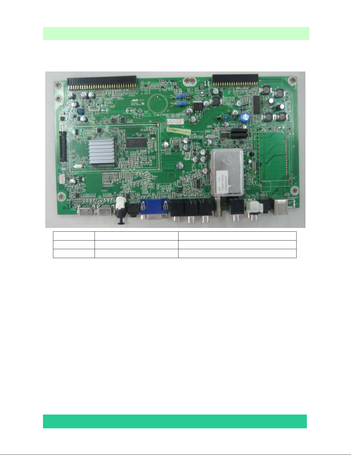
4.2 Main BD
CON8
LCD TV Service Manual
CON10
Location No.
CON10 PH2.54X8.5 2X30P 90\ROH connect Main BD and Terminal BD
CON8 FF-HX19-10\ROH LVDS
SPECIFICATION
Description
Hisense Confidential
- 15 -
Page 16
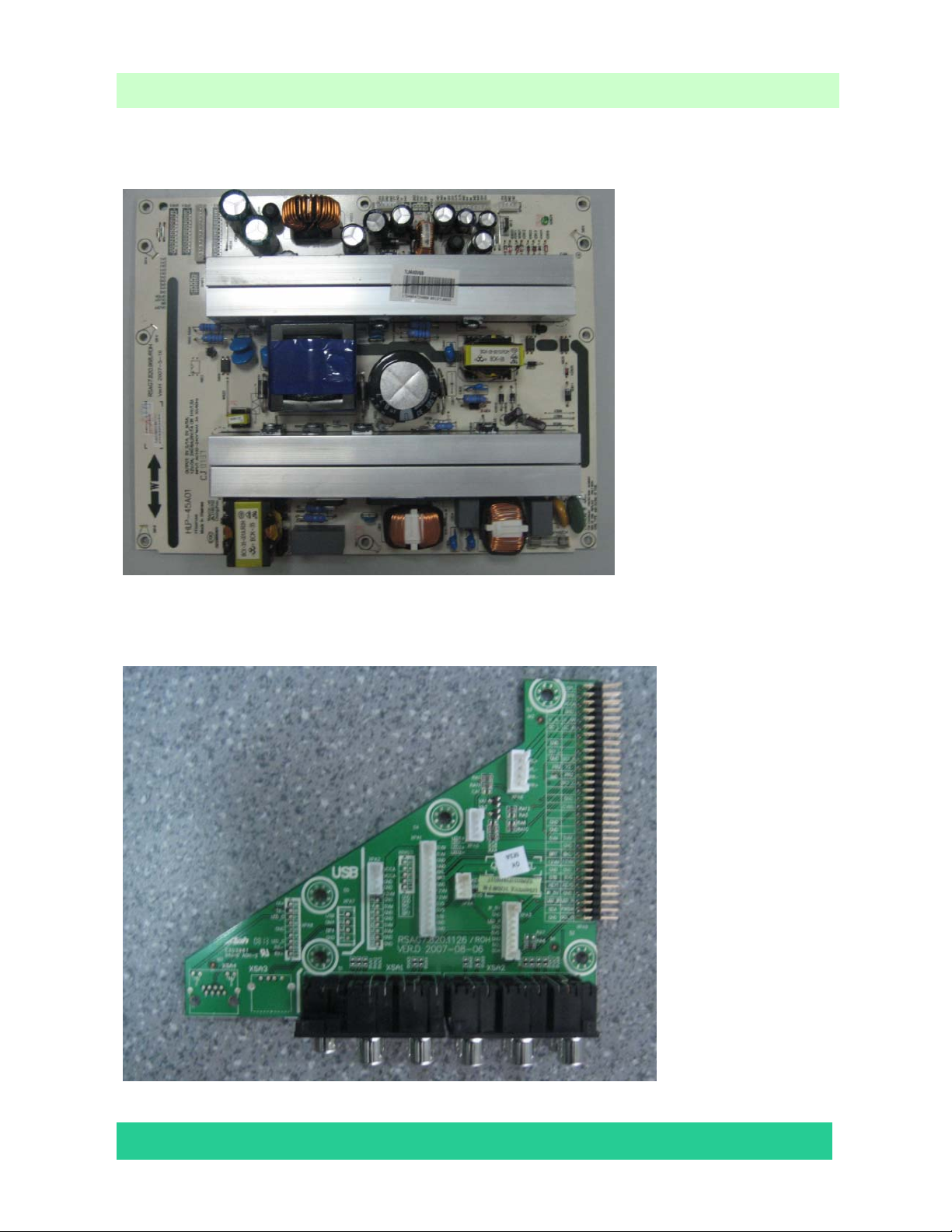
4.3 Power BD
LCD TV Service Manual
4.4 Terminal Board
Hisense Confidential
- 16 -
Page 17
LCD TV Service Manual
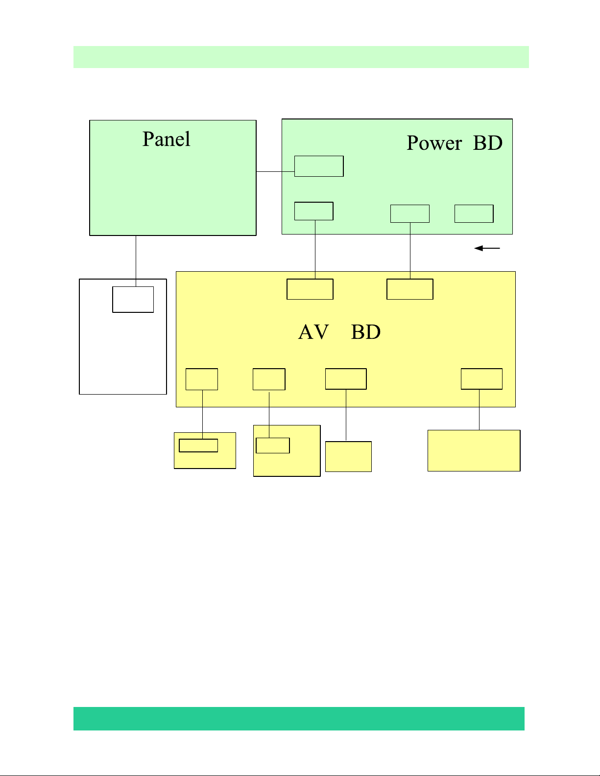
4.4 Wires and Cables Overall Wiring Diagrams
CON8
Main BD
(7)
XPA4
(5) (6)
3 Pin
xpk1
Key BD
(2)
XPA3
8pin
XP113
IR BD
XP809
XP808
4Pin
XPA2
(4)
XPA6
Speakers
(8)
XP812
14Pin
(3)
XPA1
XP801
3pin
(1)
XPA5
(9)
luminophor
Hisense Confidential
- 17 -
Page 18

No DESCRIPTION SPECIFICATION NOTE
Main Power TJC2-3Y-350-2\ROH Power Inlet-->Power BD XP801
1
LCD TV Service Manual
2
Back light power to panel
5V,12V power and communication
3
between Terminal BD and power BD
Audio amplify TJC10T-4Y-250\ROH Power BD XP808<--> Terminal BD XPA2
4
Buttons TJC10T-3Y-1100\ROH Terminal BD XPA4<--> Key BD XPK1
5
IR TJC10T-8Y-700\ROH Terminal BD XPA3<-->IR BD XP113
6
LVDS signal HX2-2X15KLB600P-SAM\ROH Main BD CON8<-->Panel
7
Audio( input/output) TJC3H-4Y-500-900\ROH Terminal BD XPA6<--> Speaker
8
9
luminophor
HX-3006B550\ROH Power BD XP809<--> Panel backlight port
TJC10T-14Y-250\ROH Power BD XP812<--> Terminal BD XPA1
B-700-500 Terminal BD XPA5<-->Luminophor
Hisense Confidential
- 18 -
Page 19

LCD TV Service Manual
5. Factory/Service OSD Menu and Adjustment
5.1 To enter the Factory OSD Menu
a. With factory RC (remote control)
1. Press “M” button and enter factory mode.
2. Press “Menu” button and enter factory OSD menu.
3 . Press “CH+”/“CH-” button select the function menu, press “VOL+”/“VOL-” enter the
selected function menu. Press “VOL+”/“VOL-” button adjust values in the menu.
4. Press “M” button exit factory mode in the factory OSD menu.
When TV outgoing factory,user can not enter factory OSD menu with Factory Remote
b. With user’s RC
1. Power TV On
2. Press Menu button and call up User OSD Menu
3. Select Sound-> Balance
4. When Balance value is “0”,Enter 0->5->3 ->2 in sequence.
Note: If necessary, re-do number keys.
5. Factory OSD appears.
6. Press the standby button then AC turn off and restart the TV, which can ex it factory OSD
menu.
5.2 Factory OSD Menu
The Factory OSD Menu comprises Factory Menu and Design Menu .
5.2.1、Factory Menu
Factory Menu
White Balance
Auto Test
Auto Calibration
LOGO
OSD Language
Country
Option
Factory Init
Test Pattern
Version:
Hisense Confidential
- 19 -
White Balance
R DRV 8
G DRV 10
B DRV 10
R CUT 136
G CUT 130
B CUT 121
BRIGHT_H 80
CONTRAST _H 80
BRIGHT_L 40
CONTRAST_L 40
Page 20

LCD TV Service Manual
Auto Calibration
Auto Color
Color Temp. Standard
RED COLOR 136
GREEN COLOR 130
BLUE COLOR 121
Option
SOURCE TV
BRIGHT 0 10
BRIGHT 50 100
BRIGHT 100 150
CONTRAST 0 60
CONTRAST 50 100
CONTRAST 100 150
TOFAC M
HDMI Cable Standard
DQS PHASE 3
LOGO
NULL
HISENSE
WELCOME
Factory Init
QingDao
HuangDao
Guiyang
shunde
Hungary
France
Australia
CLEAR PROTECTLY
CLEAR UNPROTECTLY
Turkey
Hisense Confidential
- 20 -
Page 21

LCD TV Service Manual
Test Pattern
BLUE
5.2.2、Design Menu
Design Menu
Picture Mode
Sound Mode
Sound Settings
Power Save
PIP Option
EMI
MOVESHARPNESS
LipSync
Version
Version:
LCD40V57CA_VER1.00.200806X
Panel Type:
SAM 40 (1366*768)
FLASH :
PS25P40
Hisense Confidential
- 21 -
Page 22

LCD TV Service Manual
Picture Mode
Standard Brightness 50
Contrast 50
Colour 50
Bright Brightness 60
Contrast 60
Colour 55
Soft Brightness 45
Contrast 45
Colour 45
Sound Settings
VOLUME 0 128
VOLUME 1 79
VOLUME 20 27
VOLUME 40 23
VOLUME 100 8
TVPRE SCALER 6
VOLUME SCALER 0
Sound Mode
Standard 120Hz 12
500Hz 10
1.5KHz 11
5KHz 8
10KHz 15
Music 120Hz 19
500Hz 11
1.5KHz 12
5KHz 14
10KHz 20
Speech 120Hz 4
500Hz 10
1.5KHz 12
5KHz 7
10KHz 5
Note:
The abov e “Factory/Service OSD Menu” are reference only, please refer to the actual units
to determine the appearances.
Hisense Confidential
- 22 -
Page 23

LCD TV Service Manual
6. Software Upgrading
The software is upgraded by a burning tool- ISP_TOOL4.0.9, which can burn the
program file“*.bin”to the main board of the unit
6.1 Get ready for upgrading
6.1.1 Install the ISP_TOOL4.0.9-------only for the first time update.
1、 Port Setting:
Choose “system”option from the “control panel”
Hisense Confidential
- 23 -
Page 24

Click the “system” icon as the following
Choose the “hardware” option from the dialog window
LCD TV Service Manual
Hisense Confidential
- 24 -
Page 25

Click“device management” icon as the following
Choose the port (COM and LPT1)
LCD TV Service Manual
Choose the ECP print port (LPT1)
Hisense Confidential
- 25 -
Page 26

Click the port of print (LPT1)as the following
LCD TV Service Manual
Choose “port setting”option as the following
Hisense Confidential
- 26 -
Page 27

2、 Find the folder where the ISP_TOOL4.0.9 lies in.
There are three folders/files in this folder together.
DLPORTIO.dll and FTD2XX.DLL must be in the same folder
LCD TV Service Manual
Double click the ISP_TOOL4.0.9 icon, and then a dialog window will show as below .
Hisense Confidential
- 27 -
Page 28

Click the Config button. And then a dialog window will show as below.
Port Type setting is LPT1
Base Addr setting is 0x378
Draw
Speed setting is 99
As following
on the front of “pin 1 switch UART/I2c”
LCD TV Service Manual
Choose“SDA in”and setting “PIN” is “PIN10”。
Notes:
Do not draw
As following
on the front of “Reverse High”。
Hisense Confidential
- 28 -
Page 29

Choose “SCL in”and setting “PIN” is “PIN11”。
Notes:
Do not draw
As following
Choose “SDA out”and setting “PIN” is “PIN4”
Notes:
Draw
As following。
on the front of “Reverse High”。
on the front of “Reverse High”。
LCD TV Service Manual
Choose “SCL out”and setting “PIN” is “PIN2”
Notes:
Draw
As following
on the front of “Reverse High”
Hisense Confidential
- 29 -
Page 30

After having finished all above, clicking the “Apply ”button to complete the configuration。
LCD TV Service Manual
6.1.2 Hardware connecting
You can update the software through a special tool (as following)
Hisense Confidential
- 30 -
Page 31

Connect the Debug board to the TV use VGA interface, the other parallel port to the
computer, just as the following。
LCD TV Service Manual
Hisense Confidential
- 31 -
Page 32

LCD TV Service Manual
6.2 Upgrading with the ISP_TOOL4.0.9
6.2.1 Double click the ISP_TOOL4.0.9 icon and a dialog window will show as following。
Click the“Read ”button。
Hisense Confidential
- 32 -
Page 33

Choose the update file from the folder。
LCD TV Service Manual
Hisense Confidential
- 33 -
Page 34

The update file has been chosen successfully。
Click the“Auto”button and choose parameters as following。
Click the“Run”button
LCD TV Service Manual
Click the“connect”button,then show a dialog box as following。
Hisense Confidential
- 34 -
Page 35

If show above then click the“Run”button again and again,till show the following dialog
window。
LCD TV Service Manual
Hisense Confidential
- 35 -
Page 36

LCD TV Service Manual
The above appears on the screen-the word “program ok”shows in the information
displaying window,indicating upgrading is over。
6.2.2 After the update is over. Must Confirm the software Version in the Version Menu.
If the update is successful, enter Factory Init Menu and select “Clear Unprotectly”
a. Press VOL+ button to clear the EEPROM data.
b. When the “Clear Unprotectly ” b utton becomes white, turn off the power.
c. Restart the TV.
Hisense Confidential
- 36 -
Page 37

LCD TV Service Manual
7. Troubleshooting
7.1 Troubleshooting for Remote Control
Remote control does not work
YES
Try new batteries
Replace battery
NO
Replace RC
YES
Replace remote control
NO
Check IR receiver
Change Led & IR board
NO
Change Led & IR cable
YES
YES
Replace Led & IR BD
Replace Led & IR cable
NO
Replace main board
Hisense Confidential
- 37 -
Page 38

LCD TV Service Manual
7.2 Troubleshooting for Function Key
Buttons does not work
Check switches
YES
Replace tact switch
NO
Check key board
YES
Replace Key BD
NO
Check Key BD cable
Change Key BD cable
YES
OK
NO
Replace main board
Hisense Confidential
- 38 -
Page 39

7.3 TV won’t Power On
LCD TV Service Manual
TV won’t power on
Is LED light?
NO
Check Power
Inlet
YES
Make Sure Power
source is live
YES
NO
BLUE
RED
OSD?
NO
YES
Check signal
Source
YES
NO
Check Power
Cord
NO
Try Power on by
RC and Button
Neither
works
Replace Main
BD
YES
Only
one works
Both
Work
Replace
Power Cord
Check/replace IR
BD or Keypad
PCA
NO
Replace Panel
Replace Main BD
OK
YES
Power on
NO
Replace Power BD
YES
OK
Hisense Confidential
- 39 -
Page 40

LCD TV Service Manual
7.4 Troubleshooting for Audio
No sound
Check connecter
YES
Reconnect
NO
Check speaker wire
NO
Check speaker set
YES
YES
Replace speaker wir e
Replace speaker set
NO
Replace main board
YES
OK
Hisense Confidential
- 40 -
Page 41

LCD TV Service Manual
7.5 Troubleshooting for TV/VGA/HDMI input
No picture on the screen
Check Signal Source
NO
Make sure signal
source is available
Check connect
YES
Reconnect
NO
Check cable
YES
Replace cable
NO
Replace main board
Hisense Confidential
- 41 -
Page 42

LCD TV Service Manual
7.6 Troubleshooting for YPbPr input
No picture on the sc reen
Check Source work or not
YES
Check connect
NO
Check Wires (Green Blue, Red)
NO
Replace main board
NO
YES
YES
Check Source Device
Reconnect
Replace wires
Hisense Confidential
- 42 -
Page 43

LCD TV Service Manual
7.7 Troubleshooting for Video/S-Video/ SCART input
No picture on the screen
Check Source work or not
YES
NO
Check Signal Source
Check connect
YES
Reconnect
NO
Check Cable/ Wires
YES
Replace Cable/Wires
NO
Check SCA RT BD
YES
Replace SCART BD
NO
Replace main board
Hisense Confidential
- 43 -
Page 44

LCD TV Service Manual
8. Explode View and explode BOM List
Explode BOM List:
LCD40V57CA
No. Part Name Num. Code No. Remark
1 lamp bar unit 1 B-700-500
2 LCD PANEL 1 LTA400AA04
3 IR Board Unit 1 RSAG2.908.102
4 Key Board Unit 1 RSAG2.908.108
5 Main Board Unit 1 RSAG2.908.1101-15
6 Power Board Unit 1 RSAG2.908.982-4
7 Bracket Unit 1 RSAG6.150.349
8 Terminal bracket 1 RSAG8.041.182
9 front cover 1 RSAG8.074.467
10 Back cover 1 RSAG8.074.468
11 bracket 1 RSAG8.078.480
12 bracket 1 RSAG8.078.481
13 Terminal bracket 1 RSAG8.081.312
14 key 1 RSAG8.335.067
15 baffle 1 RSAG8.634.047
16 Lens led 1 RSAG8.640.056
17 ornament 1 RSAG8.647.247
18 base unit 1 WG6.121.052
19 speaker 2 YDT415E-10W8R-F
20 Screw 23 SJ2836-87 M3X8
21 Screw 2 GB/T 818-2000 M4X8
22 Screw 37 SJ2824-87 ST4X14F
23 Screw 4 SJ2825-87 ST3X12C
24 Screw 7 SJ2832-87 ST3X10
25 Screw 4 SJ2838-87 ST4X16C.II
26 terminal board unit 1 RSAG2.908.1153-3
27 Terminal bracket 1 RSAG8.041.182
28 scutcheon 1 RSAG8.804.3233
29 bracket 15 RSAG8.078.485
30 cover board 1 RSAG8.634.057
31 power tie 1 RSAG8.667.014
32 scutcheon 1 RSAG8.804.317
33 Screw 4 GB/T 818-2000 M6X16
Hisense Confidential
- 44 -
Page 45

9. Schematic circuit diagram
LCD TV Service Manual
Hisense Confidential
- 45 -
Page 46

LCD40V57CA
Page 47

5
POWER-ON/OFF10
Q34
D D
Q34
R337 4.7KR337 4.7K
C
C
SOT
SOT
23
23
3904
3904
E
B
E
B
R338
R338
132
4.7K
4.7K
Vcc3.3for MST6X89BL
analog
4
ADJ
OUT
ADJ
OUT
IN
C21
C21
0.1uF
0.1uF
IN
3
2
1
C360
C360
C22
C22
10uF
10uF
0.1uF
0.1uF
+3.3Vstb
L17 10uHL17 10uH
C361
C361
10uF
10uF
+3.3V for
VDDP
C C
5Vstb
C20
C20
C413
C413
0.1uF
100uF/16V
100uF/16V
0.1uF
C359
C359
10uF
10uF
AMS1117-3.3
AMS1117-3.3
L12 10uHL12 10uH
U5
U5
R336NCR336
NC
5Vstb
Normal: L
Standby:H
PW_CTL
PW_CTL 2
Vcc3.3for MST6X89BL
analog
Pin99, Pin165,
Pin183, Pin194,
Pin207, Pin221,
Pin235,
C61
C61
C357
C357
0.1uF
0.1uF
10uF
10uF
C66
C66
0.1uF
0.1uF
C67
C67
0.1uF
0.1uF
4
R341
R347 10R/2WR347 10R/2W
R341
100uF/16V
100uF/16V
10R/2W
10R/2W
CA58
CA58
C111
C111
0.1uF
0.1uF
1
2.5V for MST6X89BL
and DDRAM
AMS1117-2.5
AMS1117-2.5
5Vstb
L20 10uHL20 10uH
C69
C69
0.1uF
0.1uF
C65
C65
0.1uF
0.1uF
C68
C68
0.1uF
0.1uF
VDDP
C70
C70
0.1uF
0.1uF
+5V
C31
C31
0.1uF
0.1uF
C379
C379
10uF
10uF
L13 10uHL13 10uH
U19
U19
3
+5VA+12V
2
VOUT
VIN
GND
LM7805
LM7805
3
U8
U8
C24
C24
0.1uF
0.1uF
ADJ
ADJ
1
100uF/16V
100uF/16V
4
OUT
OUT
IN
IN
2
3
C374
C374
10uF
10uF
CA59
CA59
C25
C25
0.1uF
0.1uF
C112
C112
0.1uF
0.1uF
+2.5VM
C375
C375
10uF
10uF
ON_PANEL
ON_PANEL2
ON_PBACK2
PWM02
ON_PBACK
PWM0
+5V
2
+12V
+5V
5Vstb
5Vstb
R21 0R21 0
R17 NCR17 NC
D46
D46
SMB5818
SMB5818
R15 10KR15 10K
R5
1
4.7KR54.7K
C15
C15
0.1uF
0.1uF
1
L2
L2
NC/600(4.5X3.2)
NC/600(4.5X3.2)
L6
L6
600(4.5X3.2)
600(4.5X3.2)
L9NCL9
NC
Q2
3904Q23904
2 3
R18NCR18
NC
R13
R13
4.7K
4.7K
1
Q5
NC(3904)Q5NC(3904)
2 3
R16 47KR16 47K
R6
4.7KR64.7K
R91KR9
1K
2 3
1
Q3
3904Q33904
1
LCD Power
VPANEL_IN
1
2
3
4
C2
0.1uFC20.1uF
SAMSUNG panel 0~3.3V R34 Connect
LG/CMO/AU panel 0~5V,R34 NC
BL-ON/OFF
R14 1KR14 1K
R34
R34
NC/10K
NC/10K
BL-ADJUST
C14
C14
2.2uF
2.2uF
5Vstb
R2
10KR210K
C1
0.1uFC10.1uF
R3 1KR3 1K
Q1
2 3
3904Q13904
R12
R12
4.7K
4.7K
R11 0R11 0
Q4
3904Q43904
2 3
U2
IRF7314U2IRF7314
S1
G1
S2
G2
1
D1
D1
D2
D2
VCC-Panel
8
7
6
5
BL-ON/OFF 10
BL-ADJUST 10
C3
0.1uFC30.1uF
Vcc3.3for MST6X89BL
analog
AMS1117-3.3
AMS1117-3.3
5Vstb
L15 10uHL15 10uH
+5V
B B
+3.3AVDD for
AVDDA
+3.3Vstb
A A
L14 10uHL14 10uH
C40
C40
C384
C384
0.1uF
0.1uF
10uF
10uF
L23 FBL23 FB
+3.3AVDD AVDD_MemPLL
L18 FBL18 FB
4
U6
U6
ADJ
OUT
ADJ
OUT
IN
IN
3
2
C33
C33
0.1uF
0.1uF
1
C385
C385
10uF
10uF
C34
C34
0.1uF
0.1uF
+3.3AVDD
C386
C386
10uF
10uF
Pin14, Pin39, Pin58,Pin254
AVDDA
C23
C23
C287
C287
C58
C58
C362
C362
0.1uF
0.1uF
10uF
10uF
3.3V for
AVDDPLL2
C371
C371
10uF
10uF
5
0.1uF
0.1uF
C47
C47
0.1uF
0.1uF
0.1uF
0.1uF
Pin136
C289
C289
0.1uF
0.1uF
+3.3V for
VDD_MPLL
+3.3Vstb AVDD_MPLL
L24 FBL24 FB
+3.3AVDD
for AVDD_SIF
+3.3AVDD
+3.3AVDD
C370
C370
10uF
10uF
10nF
10nF
L19 10uHL19 10uH
+3.3AVDD for
AVDD_AU
L22 10uHL22 10uH
C372
C372
10uF
10uF
C373
C373
10uF
10uF
C60
C60
C62
C62
0.1uF
0.1uF
1 2
AVDD_SIF
Pin63
C49
C49
0.1uF
0.1uF
AVDD_AU
Pin70 Pin108, Pin114,
C51
C51
0.1uF
0.1uF
4
2.5V for DDRAM
+2.5VM +2.5V_DMC
L21 FBL21 FB
C376
C376
10uF
10uF
+2.5VM
L25 FBL25 FB
+2.5V_DMQ
C377
C377
10uF
10uF
+2.5V for MST6X89BL
L16 FBL16 FB
C378
C378
10uF
10uF
C35
C35
0.1uF
0.1uF
C50
C50
0.1uF
0.1uF
C63
C63
0.1uF
0.1uF
C36
C36
0.1uF
0.1uF
5Vstb
L79
C404
C404
100uF/16V
100uF/16V
L79
4.7uH
4.7uH
5Vstb
VCC-1.2V
C410
C410
C409
C409
100uF/16V
100uF/16V
+2.5MVDD+2.5VM
C37
C37
C38
C38
C39
C39
0.1uF
0.1uF
0.1uF
0.1uF
0.1uF
0.1uF
3
100P
100P
Pin119, Pin135, P147
D10
D10
C403
C403
100N
100N
IN4148
IN4148
5Vstb
C401
C401
10N
10N
R48 0R48 0
D30
D30
SMB5818
SMB5818
VCC-1.2V
2
U13
U13
MP2270
MP2270
MP2270
MP2270
1
BS
2
NC
3
SW
4
NC
5
IN
R479
R479
20K
20K
L8 600(4.5X3.2)L8 600(4.5X3.2)
C380
C380
10uF
10uF
R418
R418
47K
47K
11
GND
10
FB
9
NC
8
GND
7
NC
6
EN
C26
C26
0.1uF
0.1uF
Title
Title
Title
Size Document Number Rev
Size Document Number Rev
Size Document Number Rev
A3
A3
A3
Date: Sheet
Date: Sheet
Date: Sheet
C411
C411
100N
100N
VDDC
C29
C29
C28
C28
C27
C27
0.1uF
0.1uF
0.1uF
0.1uF
0.1uF
0.1uF
深圳市高新区南区科技南十路国际技术创新研究院C座4楼
深圳市高新区南区科技南十路国际技术创新研究院C座4楼
深圳市高新区南区科技南十路国际技术创新研究院C座4楼
power
power
power
MST6X89BL 01A
MST6X89BL 01A
MST6X89BL 01A
R481
R481
82K
82K
C30
C30
Pin99, Pin146, Pin182,
Pin195, Pin242
0.1uF
0.1uF
TEL:0755-26996895 FAX:0755-26996830
TEL:0755-26996895 FAX:0755-26996830
TEL:0755-26996895 FAX:0755-26996830
111Monday, December 17, 2007
111Monday, December 17, 2007
111Monday, December 17, 2007
1
of
of
of
Page 48

5
VDDP
3
R26
R26
2
D54
D54
BAV99
+3.3AVDDAVDDA
R234
R234
R235
R235
10K
10K
10K
DTV_PBIN/SC1-Bin+11
DTV_YIN/SC1-Gin+11
DTV_SOG/SC1-SOG11
DTV_PRIN/SC1-Rin+11
C436
C436
4.7uF
4.7uF
PVR-Lin/SC1-Lout
PVR-Rin/SC1-Rout
ALout/SC2-Lout
ARout/SC2-Rout
AMP-L
AMP-R
I2C_SDA
I2C_SCL
TXD0
RXD0
KEY0
KEY1
SC2-FSIN
R394
R394
4.7K
4.7K
RXD0
TXD0
10K
TX1CLK-3
TX1CLK+3
B1_TX0-3
B1_TX0+3
G1_TX1-3
G1_TX1+3
R1_TX2-3
R1_TX2+3
HDMI1_SDA3
HDMI1_SCL3
HDMI1_HPDCTRL3
TX2CLK-3
TX2CLK+3
B2_TX0-3
B2_TX0+3
G2_TX1-3
G2_TX1+3
R2_TX2-3
R2_TX2+3
HDMI2_SDA3
HDMI2_SCL3
HDMI2_HPDCTRL3
SC1-FSIN11
SC1-FBIN11
HS_RGB4
VS_RGB4
PB+5
DMP_SOG5
Y+5
PR+5
HDTV_PBin5
HDTV_SOG5
HDTV_Yin5
HDTV_PRin5
SV1-Cin6
SV1-Yin6
SC2-Cin111
SC2-Yin111
AV2-Vin/SC2-Vin16
SC1-Vin111
AV1-Vin+6
AV1-Vin-6
TV1-Vin+6
TV1-Vin-6
CVBSOut16
CVBSOut06
TV-SIFP7
TV-SIFM7
C435
C435
C213
C213
1uF
1uF
10uF
10uF
C271
C271
R345
R345
R406
R406
C270
C270
C188
C188
2.2nF
2.2nF
22K
22K
22K
22K
2.2nF
2.2nF
2.2nF
2.2nF
+3.3Vstb
R460
R460
10K
10K
R462
R462
10K
10K
5
D D
C C
B B
A A
TJC10-4A
TJC10-4A
HDMI1_HPDCTRL
HDMI2_HPDCTRL
DVI/HDMI
INPUT
SCART
INPUT
VGA/DMP
INPUT
HDTV
INPUT
VIDEO
INPUT
AUDIO
INPUT
PVR-Lin/SC1-Lout6
PVR-Rin/SC1-Rout6
ALout/SC2-Lout6
ARout/SC2-Rout6
AMP-L8
AMP-R8
AUDIO
OUTPUT
TXD04
RXD04
SC2-FSIN11
5Vstb
R384
R384
5Vstb
CN10
CN10
1
4.7K
4.7K
2
3
4
BAV99
10K
10K
1
R170 1KR170 1K
C206
C206
10uF
10uF
TX1CLKTX1CLK+
B1_TX0B1_TX0+
G1_TX1G1_TX1+
R1_TX2R1_TX2+
HDMI1_SDA
HDMI1_SCL
HDMI1_HPDCTRL
TX2CLK-
TX2CLK+
B2_TX0B2_TX0+
G2_TX1G2_TX1+
R2_TX2R2_TX2+
HDMI2_SDA
HDMI2_SCL
HDMI2_HPDCTRL
C812 0.1uFC812 0.1uF
C814
C814
DTV_PBIN/SC1-Bin+
DTV_YIN/SC1-Gin+
DTV_SOG/SC1-SOG SOGIN0
DTV_PRIN/SC1-Rin+
SC1-FSIN
SC1-FBIN
HS_RGB
VS_RGB
PB+
DMP_SOG
Y+
PR+
HDTV_PBin
HDTV_SOG
HDTV_Yin
HDTV_PRin
SV1-Cin
SC2-Cin1
SC2-Yin1
SC1-Vin1
AV1-Vin+ CVBS1AV1-Vin+
TV1-Vin+
TV1-VinCVBSOut0
C437
C437
MUX-Lin19
MUX-Rin19
0.1uF
0.1uF
AV1+S1-Lin6
AV1+S1-Rin6
SC1-Lin111
SC1-Rin111
AV2-Lin/SC2-Lin16
AV2-Rin/SC2-Rin16
RP35
RP35
5678
5678
RP100X4
RP100X4
R352
R352
R272
R272
C172
C172
C154
C154
C176
C176
R293
R293
22K
22K
22K
22K
2.2nF
2.2nF
10nF
10nF
10nF
10nF
22K
22K
RP37
RP37
RP100X4
RP100X4
+12V
R53 47R53 47
PWM2
R442
R442
10K
10K
PWM0
PWM0 1
PWM1
PWM2
PWM3
R456
R456
10K
10K
CA110
CA110
100uF/16V
100uF/16V
Q14
Q14
1
3906
3906
SYS_RST
R27 1KR27 1K
3 2
C263
C263
R172
R172
27pF
27pF
10K
10K
C356
C356
27pF
27pF
12MHz for USB
TX1CLK-
AVDDA
TX1CLK+
B1_TX0B1_TX0+
R454
R454
G1_TX1G1_TX1+
R1_TX2R1_TX2+
390_1%
390_1%
HDMI1_HPDCTRL
HDMI1_SDA
HDMI1_SCL
TX2CLK-
TX2CLK+
B2_TX0B2_TX0+
G2_TX1-
G2_TX1+
R2_TX2-
R2_TX2+
HDMI2_HPDCTRL
HDMI2_SDA
HDMI2_SCL
C358 0.1uFC358 0.1uF
C813NCC813
NC
0.1uF
0.1uF
AV1+S1-Lin
AV1+S1-Rin
SC1-Lin1
SC1-Rin1
AV2-Lin/SC2-Lin1 AUL3
AV2-Rin/SC2-Rin1
4321
4321
RP36
RP36
RP100X4
RP100X4
R351
R351
22K
22K
5678
5678
L28 100uHL28 100uH
R51 4.7KR51 4.7K
0.1uF
0.1uF
C815
C815
0.1uF
0.1uF
C816
C816
DTV_PBIN/SC1-Bin+
C182 47nFC182 47nF
DTV_YIN/SC1-Gin+
C183 47nFC183 47nF
DTV_SOG/SC1-SOG
C178 47nFC178 47nF
C153 1nFC153 1nF
SC1-FSIN
SC1-FBIN
HS_RGB
VS_RGB
PB+
C133 47nFC133 47nF
DMP_SOG
C136 1nFC136 1nF
Y+
C134 47nFC134 47nF
PR+
C135 47nFC135 47nF
HDTV_PBin
C157 47nFC157 47nF
HDTV_SOG
C159 1nFC159 1nF
HDTV_Yin
C158 47nFC158 47nF
HDTV_PRin
C156 47nFC156 47nF
SV1-Cin
C316 47nFC316 47nF
SV1-YinSV1-Yin
C317 47nFC317 47nF
C323 47nFC323 47nF
C324 47nFC324 47nF
C312 47nFC312 47nF
SC1-Vin1
C311 47nFC311 47nF
C320 47nFC320 47nF
C322 47nFC322 47nF
TV1-Vin+
C308 47nFC308 47nF
TV1-Vin-
C214 47nFC214 47nF
CVBSOut1CVBSOut1
CVBSOut0
TV-SIFP SIF0P
C440 0.1uFC440 0.1uF
TV-SIFM
C441 0.1uFC441 0.1uF
AUVREF
AUVRADP
AUVRADN
MUX-Lin1
C332 2.2uFC332 2.2uF
MUX-Rin1
C333 2.2uFC333 2.2uF
C334 2.2uFC334 2.2uF
C335 2.2uFC335 2.2uF
R663 0R663 0
C434 0.1uFC434 0.1uF
C336 2.2uFC336 2.2uF
C337 2.2uFC337 2.2uF
C339 2.2uFC339 2.2uF
C338 2.2uFC338 2.2uF
LINE_OUT_0L
LINE_OUT_0R
LINE_OUT_1L
LINE_OUT_1R
DAC_OUT_0L
4321
5678
4321
5678
DAC_OUT_0R
DAC_OUT_1L
DAC_OUT_1R
4321
4321
D42
D42
Q44
Q44
2SC1815
2SC1815
PWM1
R52 33KR52 33K
CL=20pf of XTAL
Y4
6MHZY46MHZ
1 2
10
12
13
15
16
18
19
20
21
22
23
252
253
255
256
VCLAMP
26
REFP
27
REFM
28
VCOM3VCOM3
33
VCOM2
35
BIN0P
34
GIN0P
36
37
RIN0PDTV_PRIN/SC1-Rin+
38
41
42
24
25
BIN1P
29
SOGIN1
30
GIN1P
31
RIN1P
32
43
BIN2P
44
SOGIN2
45
GIN2P
46
RIN2P
47
C1
48
Y1
49
C0SC2-Cin1
50
Y0SC2-Yin1
51
CVBS3AV2-Vin/SC2-Vin1AV2-Vin/SC2-Vin1
52
CVBS2
53
54
VCOM1AV1-Vin-AV1-Vin-
55
CVBS0
56
VCOM0
57
59
60
62
64
SIFM
65
69
68
67
AUL0
71
AUR0
72
AUL1
73
AUR1
74
AUCOM
75
AUL2
76
AUR2
77
78
AUR3
79
80
81
82
83
84
85
86
87
88
177
178
179
180
171
172
173
174
40V
1N4148
1N4148
CA11
CA11
+
+
10uF/50V
10uF/50V
9
1
2
4
5
6
7
8
RXACKN
RXACKP
RXA0N
RXA0P
RXA1N
RXA1P
RXA2N
RXA2P
HPLUGA
REXT
DDCDA_DA
DDCDA_CK
RXBCKN
RXBCKP
RXB0N
RXB0P
RXB1N
RXB1P
RXB2N
RXB2P
HPLUGB
DDCDB_DA
DDCDB_CK
VCLAMP
REFP
REFM
VCOM3
VCOM2
BIN0P
GIN0P
SOGIN0
RIN0P
HSYNC0
VSYNC0
HSYNC1
VSYNC1
BIN1P
SOGIN1
GIN1P
RIN1P
VSYNC2
BIN2P
SOGIN2
GIN2P
RIN2P
C1
Y1
C0
Y0
CVBS3
CVBS2
CVBS1
VCOM1
CVBS0
VCOM0
CVBSOUT1
CVBSOUT0
SIF0P
SIF1P
SIFM
AUVREF
AUVRADP
AUVRADN
AUL0
AUR0
AUL1
AUR1
AUCOM
AUL2
AUR2
AUL3
AUR3
AUMONO
AUOUTL3
AUOUTR3
AUOUTL2
AUOUTR2
AUOUTL1
AUOUTR1
AUOUTL0
AUOUTR0
DDCR_DA
DDCR_CK
DDCA_DA
DDCA_CK
SAR0
SAR1
SAR2
SAR3
+3.3Vstb
R464NCR464
NC
C364
C364
0.1uF
0.1uF
R4461MR446
1M
SPI_CZ
SPI_DO
WP_Flash
250
XIN
4
C150
C150
AVDD_AU
AVDDA
14
254
AVDD_DVI
AVDD_DVI
39
58
AVDD_ADC
AVDD_ADC
VDDC
101
149
185
193
240
VDDC
VDDC
VDDC
VDDC
VDDC
6X89BL
6X89BL
1nF
1nF
AVDD_SIF
70
63
249
248
XOUT
AVDD_AU
AVDD_SIF
HWRESET
VDDP
165
183
VDDP
VDDP99VDDP
+2.5MVDD
194
207
221
235
108
VDDP
VDDP
VDDP
VDDP
VDDM
U41
U41
MST6X89BL
GND
GND
GND
GND
GND
GND
GND
SCK
SDI
SCZ
PWM0/MCUCFG0
PWM1/MCUCFG1
PWM3/MCUCFG3
PWM2/MCUCFG2
175
176
192
191
PWM2
PWM3
PWM0
PWM1
C365100pF C365100pF
L67 FBL67 FB
C352
C352
10uF
10uF
U42
U42
PMC25L040/MX25L4005 PMC25L080/MX25L8005
1
CE#
VDD
2
SO
HOLD#
3
WP#
SCK
VSS4SI
EN25F40
EN25F40
4
SDO
IRIN
167
168
169
170
182
SDI
SDO
SCZ
SCK
5678
5678
C387NC/10pF C387NC/10pF
R453100 R453100
4321
4321
SPI_CK
SPI_DI
SPI_CZ
SPI_DO
IR
C363
C363
0.1uF
0.1uF
SPI_CZ
8
SPI_DO
7
SPI_CK
WP_Flash SPI_CK
6
SPI_DI
5
3
RP19
RP19
RP100X4
RP100X4
GND
GND
GND
40
61
1
2
3
66
100
105
113
U44
U44
CE#
SO
WP#
VSS4SI
NC/EN25F80
NC/EN25F80
134
HOLD#
GND
148
VDD
SCK
11
17
AVDD_MemPLL
114
119
135
VDDM
VDDM
VDDM
GND
GND
GND
166
184
208
8
7
6
5
147
VDDM
GND
GND
222
241
SPI_DI
AVDD_MPLL
136
251
AVDD_MPLL
AVDD_MEMPLL
GND
257
3
R706 NCR706 NC
96
98
97
GPIOF[9]
GPIOF[8]
AD[5]
AD[6]
GPIOB[4]/UART1_RX
AD[1]
AD[2]
AD[3]
AD[4]
AD[0]
159
160
186
155
156
157
158
154
When use URAT1,P12,P13 Cann't be used again
189
190
188
187
USB_DP
USB_DM
GPIOF[0]89GPIOF[1]90GPIOF[2]91GPIOF[3]92GPIOF[4]93GPIOF[5]94GPIOF[6]95GPIOF[7]
OTG_CID
OTG_VBUS
247
DI[13]
246
DI[12]
245
DI[11]
244
DI[10]
243
DI[9]
242
DI[8]
239
DI[7]
238
DI[6]
237
DI[5]
236
DI[4]
234
DI[3]
233
DI[2]
232
DI[1]
231
DI[0]
230
IVSYNC
229
IHSYNC
228
IDE
227
ICLK
LVSYNC/GPIOE[0]
LVHSYNC/GPIOE[1]
AD[7]
WRZ
161
163
162
226
225
224
LDE/GPIOE[2]
223
LCK/GPIOE[3]
220
LVB0M
219
LVB0P
218
LVB1M
217
LVB1P
216
LVB2M
215
LVB2P
214
LVBCKM
213
LVBCKP
212
LVB3M
211
LVB3P
210
LVB4M/NC
209
LVB4P/NC
206
LVA0M
205
LVA0P
204
LVA1M
203
LVA1P
202
LVA2M
201
LVA2P
200
LVACKM
199
LVACKP
198
LVA3M
197
LVA3P
196
LA4M/NC
195
LVA4P/NC
123
MDATA[0]
122
MDATA[1]
121
MDATA[2]
120
MDATA[3]
118
MDATA[4]
117
MDATA[5]
116
MDATA[6]
115
MDATA[7]
112
MDATA[8]
111
MDATA[9]
110
MDATA[10]
109
MDATA[11]
107
MDATA[12]
106
MDATA[13]
104
MDATA[14]
103
MDATA[15]
130
MCLK
129
MCLKZ
128
MCLKE
127
MVREF
126
UDQM
125
LDQM
124
DQS[0]
102
DQS[1]
133
RASZ
137
CASZ
138
WEZ
131
BARD[1]
132
BARD[0]
153
MADR[11]
152
MADR[10]
151
MADR[9]
150
MADR[8]
146
MADR[7]
145
MADR[6]
144
MADR[5]
143
MADR[4]
142
MADR[3]
141
MADR[2]
140
MADR[1]
139
MADR[0]
ALE
INT
RDZ
164
181
GPIOD OTG_HOST_DET
R448 100R448 100
P42
R467 0R467 0
P41
R468 0R468 0
P40
P16
P15 HDCEC
P14
P11
P10
IO_USB_Only
3
R762NCR762
NC
MVREF
R449 100R449 100
R450 100R450 100
R452 100R452 100
R483 100R483 100
R485 22R485 22
R486 22R486 22
R487 22R487 22
5Vstb
R755
R755
10K
10K
VBUS
RP4.7KX4
RP4.7KX4
HD-VSW1
LEDR
LEDB
SPDIF
HD-VSW0
A-SW1A-SW1
A-SW0
HPDET
ON_PANEL
ON_PBACK
WP_KEY
WP_EEP
PW_CTL
TXD1
RXD1
BRI_EXT/DIS/DISPEN
OTG_OC_DET
5678
5678
5678
5678
5678
5678
5678
5678
5678
5678
5678
5678
5678
5678
5678
5678
R148
R148
R756
R756
10K
10K
10K
10K
4321
4321
4321
4321
4321
4321
4321
4321
4321
4321
4321
4321
4321
4321
4321
4321
RP38
RP38
5678
5678
4321
4321
OTG_HOST_DET
RXO0RXO0+
RXO1RXO1+
RXO2RXO2+
RXOCRXOC+
RXO3RXO3+
RXO4RXO4+
RXE0RXE0+
RXE1RXE1+
RXE2RXE2+
RXECRXEC+
RXE3RXE3+
RXE4RXE4+
MDATA0
RP28
RP28
RP100X4
RP100X4
MDATA1
MDATA2
MDATA3
MDATA4
RP29
RP29
RP100X4
RP100X4
MDATA5
MDATA6
MDATA7
MDATA8
RP30
RP30
RP100X4
RP100X4
MDATA9
MDATA10
MDATA11
MDATA12
RP31
RP31
RP100X4
RP100X4
MDATA13
MDATA14
MDATA15
MCLK+
RP32
RP32
RP33X4
RP33X4
MCLKCKE
UDQM
LDQM
DQS0
DQS1
RASZ
CASZ
WEZ
BA1
BA0
AR11
RP39
RP39
RP100X4
RP100X4
AR10
AR9
AR8
AR7
RP40
RP40
RP100X4
RP100X4
AR6
AR5
AR4
AR3
RP41
RP41
RP100X4
RP100X4
AR2
AR1
AR0
+3.3Vstb
5678
5678
RP24
RP24
RP4.7KX4
RP4.7KX4
4321
4321
5678
5678
4321
4321
+3.3Vstb
RP34
RP34
5678
5678
4321
4321
RP4.7KX4
RP4.7KX4
RP25
RP25
RP4.7KX4
RP4.7KX4
SCL3/IO3
SDA3/IO4
SDA2/AI
AMP-MUTE
SCL_EXT
SDA_EXT
ON_USB
RP33
RP33
5678
5678
4321
4321
RP4.7KX4
RP4.7KX4
A-SW1 9
A-SW0 9
HPDET 8
ON_PANEL 1
ON_PBACK 1
WP_KEY 3
PW_CTL 1
TXD1 10
RXD1 10
SCL3/IO3 10
SDA3/IO4 10
HDCEC 3
AMP-MUTE 8
SCL_EXT 7,10
SDA_EXT 7,10
ON_USB 10
HD-VSW1 5
SPDIF 2
HD-VSW0 5
+3.3Vstb
RP26
RP26
5678
5678
4321
4321
RP4.7KX4
RP4.7KX4
ANTPWR_ON/OFF
AD[5] or WRZ Pin is for
HDMI CEC funciton
control using.
2
+3.3Vstb
R102 NC/4.7KR102 NC/4.7K
+3.3Vstb
R333
R333
R329
R329
R328
NC/4.7K
NC/4.7K
I2C_SDA
I2C_SCL
IO1
IO1 10
IO2
IO2 10
ANTPWR_ON/OFF 7
SCL_EXT SDA_EXT
SCL2/LVDS_SL
BRI_OUT
MDATA15
MDATA14
MDATA13
MDATA12
MDATA11
MDATA10
MDATA9
MDATA8
DQS1
UDQM
WEZ
CASZ
RASZ
BA0
BA1 AR9
AR10
AR0
AR2 AR5
2
R328
NC/4.7K
NC/4.7K
NC/0
NC/0
R327
R327
IIC LEVEL SHIFTER
NC/0
NC/0
1
NC/2N7002
NC/2N7002
Q23
Q23
32
R321 0R321 0
R322 0R322 0
VBUS
R707 15KR707 15K
CA10
CA10
C46
C46
0.1uF
0.1uF
100uF/16V
100uF/16V
VCC-Panel
2
R767 NCR767 NC
R766 NCR766 NC
+2.5V_DMC +2.5V_DMQ
C142
C142
0.1uF
0.1uF
+2.5V_DMC +2.5V_DMQ
4
6
8
14
RXO0+
16
RXO1+
18
RXO2+
20
RXOC+
RXO3+
24
RXO4+
26
28
RXE0+
30
RXE1+
32
RXE2+
34
RXEC+
RXE3+
38
RXE4+
40
C140
C140
C122
C122
0.1uF
0.1uF
0.1uF
0.1uF
U12
U12
1
MVDD
2
DQ0
3
VDDQ
4
DQ1
5
DQ2
6
VSSQ
7
DQ3
8
DQ4
9
VDDQ
10
DQ5
11
DQ6
12
VSSQ
13
DQ7
14
NC
15
VDDQ
16
LDQS
17
NC
18
MVDD
19
NC
20
LDM
21
WE
22
CAS
23
RAS
24
CS
25
NC
26
BA0
27
BA1
28
A10/AP
29
A0
30
A1
31
A2
32
A3
33
MVDD
HY5DU281622ET-4
HY5DU281622ET-4
+2.5V_DMQ +2.5MVDD
R209
R209
FSVREF MVREF
10K
10K
R243
R243
C121
C121
0.1uF
0.1uF
10K
10K
EEP_SDA
1
NC/2N7002
NC/2N7002
Q24
Q24
EEP_SCL
32
OTG_OC_DETOTG_OC_DET
R701
R701
100K
100K
CN8
CN8
VCC
VCC
GND
GND
LVDS_SL/SCL10AI/SDA
BRI_OUT12BRI_EXT/DIS
GND
TXA0+
TXA1+
TXA2+
TXAC+22TXACTXA3+
TXA4+
GND
TXB0+
TXB1+
TXB2+
TXBC+36TXBCTXB3+
TXB4+
C138
C138
C141
C141
0.1uF
0.1uF
0.1uF
0.1uF
66
VSS
65
DQ15
64
VSSQ
63
DQ14
62
DQ13
61
VDDQ
60
DQ12
59
DQ11
58
VSSQ
57
DQ10
56
DQ9
55
VDDQ
54
DQ8
53
NC
52
VSSQ
51
UDQS
50
NC
49
VREF
48
VSS
47
UDM
46
CLK
45
CLK
44
CKE
43
NC
42
NC
41
A11
40
A9
39
A8
38
A7
37
A6
36
A5
35
A4
34
VSS
R655
R655
10K
10K
R654
R654
C120
C120
1nF
1nF
10K
10K
VCC
VCC
GND
GND
GND
TXA0TXA1TXA2-
TXA3TXA4-
GND
TXB0TXB1TXB2-
TXB3TXB4-
40P-2X20
40P-2X20
C685
C685
1nF
1nF
C137
C137
0.1uF
0.1uF
MCLKMCLK+
CKE
R104 4.7KR104 4.7K
R103 4.7KR103 4.7K
U21
U21
1
A0
2
A1
3
A2
GND4SDA
24C04
24C04
1
3
R765 NCR765 NC
5
R763 NCR763 NC
7
R764 NCR764 NC
9
11
13
RXO0-
15
RXO1-
17
RXO2-
19
RXOC-
21
RXO3-
23
RXO4-
25
27
RXE0-
29
RXE1-
31
RXE2-
33
RXEC-
35
RXE3-
37
RXE4-
39
R782 NCR782 NC
BRI_OUT
C123
C123
C139
C139
0.1uF
0.1uF
0.1uF
0.1uF
MDATA0
MDATA1
MDATA2
MDATA3
MDATA4
MDATA5
MDATA6
MDATA7
DQS0
FSVREF
LDQM
R208
R208
150_1%
150_1%
AR11
AR8
AR7
AR6AR1
AR4AR3
KEY0
KEY1
C117
C117
C684
C684
100pF
100pF
0.1uF
0.1uF
Title
Title
Title
<Title>
<Title>
<Title>
Size Document Number Rev
Size Document Number Rev
Size Document Number Rev
MST6X89BL <RevCode>
A2
MST6X89BL <RevCode>
A2
MST6X89BL <RevCode>
A2
Date: Sheet
Date: Sheet
Date: Sheet
U43
U43
1
A0
2
A1
3
A2
GND4SDA
24C64
24C64
VCC
WP
SCL
LEDR
LEDB
C116
C116
1000pF
1000pF
R692
R692
15K
15K
1
R477
R477
0/NC
0/NC
VCC
WP
SCL
+3.3Vstb
8
7
6
5
BRI_EXT/DIS/DISPEN
SCL2/LVDS_SL
R135 4.7KR135 4.7K
R159 0R159 0
R158 4.7KR158 4.7K
R431 100R431 100
R428 1KR428 1K
R434 1KR434 1K
R656
R656
C73
C73
1000pF
1000pF
15K
15K
INPAQ_VPORT
INPAQ_VPORT
1
5Vstb
R4760R476
0
R475
R475
4.7K
4.7K
8
7
6
5
SDA_OUT8
SCL_OUT8
R478
R478
0/NC
0/NC
R484
R484
WP_KEY
4.7K
4.7K
EEP_SCL
EEP_SDA
SDA2/AI
R268
R268
BRI_OUT
R269NCR269
+3.3Vstb VCC-Panel
R278NCR278
NC
R270
R270
27K
27K
R271
R271
10K
10K
5Vstb
R413
R413
4.7K
4.7K
Q46
Q46
1
3904
3904
2 3
5Vstb
R524
R524
4.7K
4.7K
Q48
Q48
1
3904
3904
2 3
+3.3Vstb
R430
R430
8.2K
8.2K
D132
D132
INPAQ_VPORT
INPAQ_VPORT
1 2
D401
D401
IN4148/NC
IN4148/NC
C306
C306
0.1uF
0.1uF
WP_EEP
SDA_OUT
SCL_OUT
5Vstb
R4800R480
0
EEP_SCL 10
EEP_SDA 10
+3.3Vstb
4.7K
4.7K
NC
LED_R
LED_B
IR_SYNCIR
KEY0-inKEY0-in
KEY1-in
D133
D133
1 2
INPAQ_VPORT
INPAQ_VPORT
R470
R470
4.7K
4.7K
R319 NCR319 NC
R320 NCR320 NC
R433
R433
8.2K
8.2K
D131
D131
1 2
211Wednesday, December 19, 2007
211Wednesday, December 19, 2007
211Wednesday, December 19, 2007
R471
R471
4.7K
4.7K
EEP_SCL
EEP_SDA
D402
D402
IN4148/NC
IN4148/NC
LED_R 10
LED_B 10
IR_SYNC 10
KEY0-in 10
KEY1-in 10
of
of
of
Page 49

5
HDMI1/5V
R781KR78
1K
HDMI1-RX2+
HDMI1-RX2HDMI1-RX1+
HDMI1-RX1HDMI1-RX0+
HDMI1-RX0HDMI1-RXC+
HDMI1-RXC-
HDMI1-HPD
HDMI1-DDC-SCL
HDMI1-DDC-SDA
D98
D98
1 2
INPAQ_EGA
INPAQ_EGA
INPAQ_VPORT
INPAQ_VPORT
1 2
P1
P1
20
21
22
D D
23
24
C C
DATA2+
DATA2 SHIELD
DATA2-
DATA1+
GND1
DATA1 SHIELD
DAT1A-
GND2
DATA0+
DATA0 SHIELD
GND3
DATA0-
GND4
CLK SHIELD
GND5
DDC/CEC GND
+5V POWER
HOT PLUG
HDMI_J
HDMI_J
CLK+
CLK-
CEC
NC
SCL
SDA
1
2
3
4
5
6
7
8
9
10
11
12
13
14
15
16
17
18
19
CEC
4
D11
D11
INPAQ_VPORT
INPAQ_VPORT
D12
D12
1 2
INPAQ_EGA
INPAQ_EGA
+5VA
1
2
D100
D100
1 2
D13
D13
1 2
INPAQ_EGA
INPAQ_EGA
D19
D19
3
BAT54C
BAT54C
Q8
Q8
C
C
23
23
SOT
SOT
B
B
132
1 2
INPAQ_EGA
INPAQ_EGA
R79
R79
10K
10K
D20
D20
5.6V
5.6V
E
E
1 2
3904
3904
D14
D14
INPAQ_EGA
INPAQ_EGA
R80
R80
10K
10K
D21
D21
5.6V
5.6V
1 2
D15
D15
1 2
R82 100R82 100
R83 100R83 100
R87 1KR87 1K
1 2
INPAQ_EGA
INPAQ_EGA
3
D16
D16
D17
D17
1 2
INPAQ_EGA
INPAQ_EGA
R81
R81
4.7K
4.7K
HDMI1_SCL
HDMI1_SDA
HDMI1_HPDCTRL
R310 10R310 10
R311 10R311 10
R312 10R312 10
R313 10R313 10
R314 10R314 10
R315 10R315 10
R696 10R696 10
R697 10R697 10
D18
D18
1 2
INPAQ_EGA
INPAQ_EGA
U14
U14
8
VCC
7
WP
6
SCL
5
R85 NCR85 NC
SDA
24C02
24C02
GND
R1_TX2+
R1_TX2G1_TX1+
G1_TX1B1_TX0+
B1_TX0TX1CLK+
TX1CLK-
WP_KEY
1
NC
2
NC
3
NC
4
HDMI1_SCL 2
HDMI1_SDA 2
HDMI1_HPDCTRL 2
WP_KEY 2
C124
C124
0.1uF
0.1uF
2
R1_TX2+ 2
R1_TX2- 2
G1_TX1+ 2
G1_TX1- 2
B1_TX0+ 2
B1_TX0- 2
TX1CLK+ 2
TX1CLK- 2
U46
U46
CEC
R664 0R664 0
HDCEC2
HDCEC
R665
R665
NC/1K
NC/1K
NC/FSA2156
NC/FSA2156
1
A
2
GND
3
B
R667 27KR667 27K
For CEC Leakage Protect
1
V+
NC
SEL
+3.3AVDD
R666
R666
6
5
10K
10K
4
P2
P2
20
21
22
23
B B
24
A A
DATA2+
DATA2 SHIELD
DATA2-
DATA1+
GND1
DATA1 SHIELD
DAT1A-
GND2
DATA0+
DATA0 SHIELD
GND3
DATA0-
GND4
CLK SHIELD
GND5
DDC/CEC GND
+5V POWER
HOT PLUG
HDMI_J
HDMI_J
CLK+
CLK-
CEC
NC
SCL
SDA
1
2
3
4
5
6
7
8
9
10
11
12
13
14
15
16
17
18
19
5
CEC
HDMI2-RX2+
HDMI2-RX2HDMI2-RX1+
HDMI2-RX1HDMI2-RX0+
HDMI2-RX0HDMI2-RXC+
HDMI2-RXC-
INPAQ_VPORT
INPAQ_VPORT
HDMI2/5V
R891KR89
1K
HDMI2-HPD
HDMI2-DDC-SCL
HDMI2-DDC-SDA
D102
D102
1 2
INPAQ_EGA
INPAQ_EGA
D38
D38
1 2
INPAQ_EGA
INPAQ_EGA
5Vstb
1
2
INPAQ_VPORT
INPAQ_VPORT
D37
D37
1 2
D103
D103
1 2
4
D22
D22
1 2
INPAQ_EGA
INPAQ_EGA
D34
D34
3
BAT54C
BAT54C
Q13
Q13
C
C
23
23
SOT
SOT
B
B
132
1 2
INPAQ_EGA
INPAQ_EGA
R93
R93
10K
10K
D36
D36
5.6V
5.6V
E
E
1 2
3904
3904
D24
D24
INPAQ_EGA
INPAQ_EGA
R138
R138
10K
10K
D35
D35
5.6V
5.6V
1 2
D25
D25
1 2
R94 100R94 100
R161 100R161 100
R137 1KR137 1K
1 2
INPAQ_EGA
INPAQ_EGA
D32
D26
D26
D32
1 2
INPAQ_EGA
INPAQ_EGA
R152
R152
4.7K
4.7K
HDMI2_SCL
HDMI2_SDA
HDMI2_HPDCTRL
3
R354 10R354 10
R350 10R350 10
R340 10R340 10
R356 10R356 10
R383 10R383 10
R385 10R385 10
R353 10R353 10
R355 10R355 10
D33
D33
1 2
INPAQ_EGA
INPAQ_EGA
U20
U20
8
VCC
7
WP
6
SCL
5
R160 NCR160 NC
SDA
24C02
24C02
GND
R2_TX2+
R2_TX2G2_TX1+
G2_TX1B2_TX0+
B2_TX0TX2CLK+
TX2CLK-
WP_KEY
1
NC
2
NC
3
NC
4
HDMI2_SCL 2
HDMI2_SDA 2
HDMI2_HPDCTRL 2
C132
C132
0.1uF
0.1uF
WP_KEY 2
R2_TX2+ 2
R2_TX2- 2
G2_TX1+ 2
G2_TX1- 2
B2_TX0+ 2
B2_TX0- 2
TX2CLK+ 2
TX2CLK- 2
深圳市高新区南区科技南十路国际技术创新研究院C座4楼
深圳市高新区南区科技南十路国际技术创新研究院C座4楼
深圳市高新区南区科技南十路国际技术创新研究院C座4楼
TEL:0755-26996895 FAX:0755-26996830
TEL:0755-26996895 FAX:0755-26996830
TEL:0755-26996895 FAX:0755-26996830
Title
Title
Title
HDMI
HDMI
HDMI
Size Document Number Rev
Size Document Number Rev
Size Document Number Rev
MST6X89BL 01A
A4
MST6X89BL 01A
A4
MST6X89BL 01A
A4
Date: Sheet
Date: Sheet
Date: Sheet
2
311Tuesday, December 18, 2007
311Tuesday, December 18, 2007
311Tuesday, December 18, 2007
of
of
of
1
Page 50

5
P3
P3
D D
VGA AUDIO
VGA AUDIO
7
D41
D41
6
1
2
3
IN4148
IN4148
PC-L
PC-R
INPAQ_VPORT
INPAQ_VPORT
+5VA VGA/5V
P5
15
5
10
14
4
9
13
C C
12
3
8
2
7
11
1
6
16
17
VGAP5VGA
R111 100RR111 100R
B B
VGA-SDA
4
D86
D86
1 2
INPAQ_VPORT
INPAQ_VPORT
R113 100RR113 100R
VGA-B+
VGA-G+
VGA-R+
TXD0
VGA-HS
VGA-VS
R396
R396
D87
D87
R397
R397
1 2
INPAQ_VPORT
INPAQ_VPORT
TXD0 2
10K
10K
10K
10K
RXD0
D95
D95
1 2
1 2
INPAQ_VPORT
INPAQ_VPORT
D27
D27
C260
C260
R294
R294
560pF
560pF
12K
12K
RXD0 2
D96
D96
INPAQ_VPORT
INPAQ_VPORT
1 2
D28
D28
D97
D97
3
R295
R295
C259
C259
12K
12K
560pF
560pF
L38 0L38 0
L39 0L39 0
L40 0L40 0
PC-Lin
PC-Rin
R9975R99
75
PC-Lin 9
PC-Rin 9
D99
D99
INPAQ_VPORT
INPAQ_VPORT
R107
R107
R10075R100
75
1 2
R10175R101
75
C143NCC143
D101
D101
INPAQ_VPORT
INPAQ_VPORT
1 2
C198 10uFC198 10uF
C193 10uFC193 10uF
C274 10uFC274 10uF
R105 100R105 100
R106 100R106 100
R108
R108
C144NCC144
2
TXD0
RXD0
VGA/5V
+5VA
R297
R297
33k
33k
R298
R298
33k
33k
HS_RGB
VS_RGB
33k
33k
33k
33k
1
2
R316
R316
R317
R317
D23
D23
BAT54C
BAT54C
5VPI
R296
R296
33k
33k
R318
R318
33k
33k
HS_RGB 2
VS_RGB 2
VGA-DDC-5V
VGA_B
VGA_G
VGA_R
1
3
VGA_B 5
VGA_G 5
VGA_R 5
VGA-SCL
D29
D29
D31
D31
5.6V
5.6V
1 2
5.6V
5.6V
1 2
22K
22K
NC
22K
22K
NC
NC/5.6V
NC/5.6V
NC/5.6V
NC/5.6V
1 2
1 2
VGA-DDC-5V
R109
R112NCR112
C145
C145
NC/0.1uF
U16
U16
1
A A
NC
2
NC
3
NC
GND4SDA
VCC
VCLK
SCL
8
7
6
5
NC/24C02
NC/24C02
NC/0.1uF
NC
R114 NC/100R114 NC/100
R115 NC/100R115 NC/100
R109
R110
R110
NC4.7K
NC4.7K
NC/4.7K
NC/4.7K
VGA-SCL
VGA-SDA
Title
Title
Title
VGA
VGA
VGA
深圳市高新区南区科技南十路国际技术创新研究院C座4楼
深圳市高新区南区科技南十路国际技术创新研究院C座4楼
深圳市高新区南区科技南十路国际技术创新研究院C座4楼
TEL:0755-26996895 FAX:0755-26996830
TEL:0755-26996895 FAX:0755-26996830
TEL:0755-26996895 FAX:0755-26996830
R116 NC/4.7KR116 NC/4.7K
Size Document Number Rev
Size Document Number Rev
Size Document Number Rev
Date: Sheet
Date: Sheet
5
4
3
Date: Sheet
MST6X89BL 01A
A
MST6X89BL 01A
A
MST6X89BL 01A
A
411Wednesday, December 19, 2007
411Wednesday, December 19, 2007
411Wednesday, December 19, 2007
of
of
2
of
1
Page 51

5
4
3
2
1
U18
U18
PI5V330
PI5V330
U17
U17
NC/PI5V330
NC/PI5V330
R14475 R14475
VCC
GND
VCC
GND
C170NC C170NC
5VPI
C281
C281
10uF
10uF
R164
R164
33k
33k
R217
R217
33k
33k
HDTV_SOG
HDTV_Yin
HDTV_PBin
HDTV_PRin
R125 47R125 47
R126 470R126 470
R124 47R124 47
R123 47R123 47
DMP_Yin
DMP_PBin
DMP_PRin
HDTV_SOG 2
HDTV_Yin 2
HDTV_PBin 2
HDTV_PRin 2
Y+
DMP_SOG
PB+330-Pb2
PR+330-Pr2
Y+ 2
DMP_SOG 2
PB+ 2
PR+ 2
R150 470R150 470
330-Y1
R215
R215
33k
33k
R162
R162
33k
33k
330-Pb1
330-Pr1
33k
33k
R154 47R154 47
R153 47R153 47
R151 47R151 47
330-Y2
5VPI
R163
R163
R216
R216
33k
33k
4
DA
7
DB
9
DC
12
DD
16
C160
C160
0.1uF
0.1uF
8
15
EN
4
DA
7
DB
9
DC
12
DD
5VPI
16
C155
C155
0.1uF
0.1uF
8
15
EN
C169NC C169NC
R14375 R14375
R14275 R14275
HD2_YIN
HD2_PBIN
HD2_PRIN
DMP_Yin
DMP_PBin
DMP_PRin
L51 0L51 0
L52 0L52 0
L53 0L53 0
+5VA
L45 FBL45 FB
R75 NCR75 NC
R76 NCR76 NC
R77 NCR77 NC
2
S1A
5
S1B
11
S1C
14
S1D
3
S2A
6
S2B
10
S2C
13
S2D
1
IN
R84 NCR84 NC
R86 NCR86 NC
R88 NCR88 NC
2
S1A
5
S1B
11
S1C
14
S1D
3
S2A
6
S2B
10
S2C
13
S2D
1
IN
C171NC C171NC
C163NC C163NC
C166NC C166NC
HD2_Lin
HD2_Rin
R324
R324
12K
12K
HD1_Y1
HD1_Pb1
HD1_Pr1
C164NC C164NC
R13075 R13075
C175 10uFC175 10uF
C174 10uFC174 10uFL50 0L50 0
C275 10uFC275 10uF
R21275 R21275
HD1_Lin
HD1_Rin
C167 10uFC167 10uF
C168 10uFC168 10uF
C266 10uFC266 10uF
R13175 R13175
R155
R155
33k
33k
HD2_Lin 9
HD2_Rin 9
HD1_Lin 9
HD1_Rin 9
R121
R121
33k
33k
33k
33k
R132
R132
33k
33k
R122
R122
R117
R117
33k
33k
R157
R157
33k
33k
5VPI
33k
33k
R118
R118
R133
R133
33k
33k
R120
R120
33k
33k
HD2_YIN
HD2_PRIN
R156
R156
33k
33k
5VPI
R119
R119
33k
33k
HD1_YIN
HD1_PBIN
HD1_PRIN
R134
R134
33k
33k
HD1_YIN
HD1_PBIN
HD1_PRIN
HD-VSW0
HD-VSW02
VGA_G
VGA_G4
VGA_B
VGA_B4
VGA_R
VGA_R4
HD-VSW1
HD-VSW12
DMP_Y
DMP_Y10
DMP_PB10
DMP_PR10
DMP_PB
DMP_PR
白
红
红
D D
P7
P7
C C
左
左
绿
绿
中
中
蓝
蓝
右
右
红
红
B B
白
白
红
红
P9
P9
3
3
2
2
4
6
5
左
左
1
绿
绿
3
2
中
中
4
蓝
蓝
6
5
右
右
7
红
红
9
8
P6
P6
1
1
3
3
2
2
4
4
6
6
5
5
7
7
9
9
8
8
P8
P8
1
1
3
3
2
2
4
4
6
6
5
5
HD1_R
4
6
5
INPAQ_VPORT
INPAQ_VPORT
HD1_Y
1
3
2
HD1_Pb
4
6
5
HD1_Pr
7
9
8
INPAQ_VPORT
INPAQ_VPORT
HD2_Y HD2_Y1
HD2_Pb
D104
D104
1 2
INPAQ_VPORT
INPAQ_VPORT
INPAQ_VPORT
INPAQ_VPORT
HD2_L
HD2_R
D135
D135
1 2
INPAQ_VPORT
INPAQ_VPORT
HD1_L
1
1
白
D130
D130
1 2
D89
D89
1 2
INPAQ_VPORT
INPAQ_VPORT
D105
D105
1 2
INPAQ_VPORT
INPAQ_VPORT
R429 10KR429 10K
R388 10KR388 10K
D134
D134
1 2
INPAQ_VPORT
INPAQ_VPORT
R419 10KR419 10K
R387 10KR387 10K
D127
D127
1 2
INPAQ_VPORT
INPAQ_VPORT
D90
D90
1 2
1 2
INPAQ_VPORT
INPAQ_VPORT
L49 0L49 0
L54 0L54 0
D111
D111
1 2
C296
C296
560pF
560pF
C295
C295
560pF
560pF
L46 0L46 0
L47 0L47 0
L48 0L48 0
D91
D91
R325
R325
12K
12K
C290
R323
R323
12K
12K
C185NC C185NC
R18675 R18675
C290
560pF
560pF
C162NC C162NC
R12975 R12975
HD2_Pb1 HD2_PBIN
HD2_Pr1HD2_Pr
R18775 R18775
C165NC C165NC
R326
R326
C297
C297
12K
12K
560pF
560pF
DMP-R/DTV-R DMP-Rin/DTV-Rin
DMP-L/DTV-L10
A A
DMP-L/DTV-L DMP-Lin/DTV-Lin
5
R400 10KR400 10K
R378 10KR378 10K
C292
C292
560pF
560pF
R299
R299
12K
12K
C286
C286
560pF
560pF
R300
R300
12K
12K
DMP-Rin/DTV-Rin 9DMP-R/DTV-R10
DMP-Lin/DTV-Lin 9
4
深圳市高新区南区科技南十路国际技术创新研究院C座4楼
深圳市高新区南区科技南十路国际技术创新研究院C座4楼
深圳市高新区南区科技南十路国际技术创新研究院C座4楼
TEL:0755-26996895 FAX:0755-26996830
TEL:0755-26996895 FAX:0755-26996830
TEL:0755-26996895 FAX:0755-26996830
Title
Title
Title
Y,Pb,Pr Input
Y,Pb,Pr Input
Y,Pb,Pr Input
Size Document Number Rev
Size Document Number Rev
Size Document Number Rev
MST6X89BL 01A
A3
MST6X89BL 01A
A3
MST6X89BL 01A
A3
Date: Sheet
Date: Sheet
3
2
Date: Sheet
511Wednesday, December 19, 2007
511Wednesday, December 19, 2007
511Wednesday, December 19, 2007
of
of
1
of
Page 52

S-Video Input
Cin
Cin
P15
P15
Yin
Yin
GND
GND
GND
GND
GND
GND
P14B
P14B
左
左
8
SIGNAL
黄
黄
9
GND
下
下
中
中
10
SIGNAL
白
白
11
GND
右
右
12
SIGNAL
红
红
14
SIGNAL
13
GND
1
SV1-CinSV1-C
L62 0L62 0
D137
D137
C225
C225
NC/330pF
3
1
INPAQ_VPORT
INPAQ_VPORT
2
4
567
SV1-Y
INPAQ_VPORT
INPAQ_VPORT
AV1-VAV1-V
INPAQ_VPORT
INPAQ_VPORT
1 2
D138
D138
1 2
INPAQ_VPORT
INPAQ_VPORT
D107
D107
1 2
NC/330pF
L63 0L63 0
C215
C215
NC/330pF
NC/330pF
D136
D136
1 2
D106
D106
1 2
INPAQ_VPORT
INPAQ_VPORT
0
C186
C186
NC/330pF
NC/330pF
R392 10KR392 10K
R393 10KR393 10K
R180 47R180 47
R18175R181
C219
C219
NC/330pF
NC/330pF
75
R183 47R183 47
C217
C217
R18275R182
75
NC/330pF
NC/330pF
L610L61
R173 47R173 47
R17975R179
C189
C189
75
NC/330pF
NC/330pF
R17547R175
C318
C318
R306
R306
560pF
560pF
12K
12K
C319
C319
560pF
560pF
SV1-Cin 2
R669 47R669 47
0
C190
C190
NC/330pF
NC/330pF
L640L64
R668
R668
4.7k
4.7k
Q36
Q36
3904
3904
2 3
R67247R672
47
NC/330pF
NC/330pF
1
C191
C191
R670
R670
47k
47k
R671 10kR671 10k
R673
R673
8.2k
8.2k
R192 47R192 47
R19375R193
75
R195 47R195 47
TV1-Vin-
C276 2.2uFC276 2.2uF
TV1-Vin- 2
PVR-Lin/SC1-Lout
PVR-Lin/SC1-Lout 2
TV1-V TV1-Vin+
SV1-Yin
SV1-Yin 2
AV1-Vin+
AV1-Vin+ 2
AV1-Vin-
47
AV1-Vin- 2
AV1+S1-Lin
AV1+S1-Lin 2
AV1+S1-Rin
R307
R307
12K
12K
AV1+S1-Rin 2
TV Input
+12V
L60 FBL60 FB
TV1-V7 TV1-Vin+ 2
12VB
C344
C344
C817
C817
10uF
10uF
0.1uF
0.1uF
PVR_L/Scart1_L
SIGNAL
SIGNAL
SIGNAL
SIGNAL
A_Lout/Scart2_Lout
R214
R214
33K
33K
R213
R213
4.7K
4.7K
C313
C313
100uF/16V
100uF/16V
R246 33R246 33
100uF/16V
100uF/16V
CVBSOut1
C194
C194
AU_L/Scart2_L
AU_R/Scart2_R
CVBSOut1 2
C192
C192
0.1uF
0.1uF
R19975R199
PVR_R/Scart1_R
Note: The IC's
CVBSOUT level is
0.5Vp-p when input
signal is 1Vp-p, so
it must multiply
signal by four (GAIN
X 4) for 2Vp-p output
AU_L/Scart2_L
R194
R194
R196
R196
470
470
Q17
Q17
3906
3906
3 2
R198
R198
75
33K
33K
1
390
390
C307
C307
Q18
Q18
3904
3904
2 3
R202
R202
120
120
CVBSOut0
1
R201
R201
4.7K
4.7K
100uF/16V
100uF/16V
CVBSOut0 2
AU_R/Scart2_R
R407 100R407 100
1
2
GND
上
上
3
4
GND
5
7
6
GND
A_Rout/Scart2_Rout
A_Rout/Scart2_Rout
INPAQ_VPORT
INPAQ_VPORT
INPAQ_VPORT
INPAQ_VPORT
1 2
INPAQ_VPORT
INPAQ_VPORT
D120
D120
C519
C519
1nF
1nF
1 2
D121
D121
C520
C520
1nF
1nF
1 2
+12V
C238
C238
0.1uF
0.1uF
R22875R228
75
D139
D139
增加了一路视频输出给
DMP_VOUT10
DMP_VOUT
R2440R244
CN16
CN16
1
1
2
2
3
3
CON3
CON3
R2041KR204
1K
R408 100R408 100
R2051KR205
1K
Q22
Q22
1
3906
3906
3 2
R206
R206
390
390
DMP
0
R2420R242
C216 2.2uFC216 2.2uF
Location
Near RCA.
C218 2.2uFC218 2.2uF
R225
R225
470
470
Q21
Q21
1
3904
3904
2 3
R222
R222
120
120
+12V
0
R244靠近CN11;R242靠近CN16
1
R675 47R675 47
R681 47R681 47
R687 47R687 47
R674
R674
4.7k
4.7k
R676
R676
Q37
Q37
R677 10kR677 10k
47k
47k
1
3904
3904
2 3
R679
R679
R67847R678
8.2k
8.2k
47
R680
R680
4.7k
4.7k
R682
R682
Q45
Q45
47k
47k
R683 10kR683 10k
1
3904
3904
2 3
R685
R685
R68447R684
8.2k
8.2k
47
R686
R686
4.7k
4.7k
R688
R688
Q38
Q38
47k
47k
R689 10kR689 10k
1
3904
3904
2 3
R691
R691
R69047R690
8.2k
8.2k
47
PVR-Rin/SC1-Rout
C277 2.2uFC277 2.2uF
ALout/SC2-Lout
C348 2.2uFC348 2.2uF
ARout/SC2-Rout
C349 2.2uFC349 2.2uF
Title
Title
Title
Video input
Video input
Video input
Size Document Number Rev
Size Document Number Rev
Size Document Number Rev
MST6X89BL 01A
A2
MST6X89BL 01A
A2
MST6X89BL 01A
A2
Date: Sheet
Date: Sheet
Date: Sheet
PVR-Rin/SC1-Rout 2
ALout/SC2-Lout 2
ARout/SC2-Rout 2
深圳市高新区南区科技南十路国际技术创新研究院C座4楼
深圳市高新区南区科技南十路国际技术创新研究院C座4楼
深圳市高新区南区科技南十路国际技术创新研究院C座4楼
TEL:0755-26996895 FAX:0755-26996830
TEL:0755-26996895 FAX:0755-26996830
TEL:0755-26996895 FAX:0755-26996830
611Tuesday, December 18, 2007
611Tuesday, December 18, 2007
611Tuesday, December 18, 2007
of
of
of
A_Lout/Scart2_Lout11
P14A
P14A
左
左
黄
A A
SC2-Vin
AV2-V
1
1
黄
黄
3
3
2
2
中
中
白
白
右
右
红
红
AV2-L
4
4
6
6
5
5
AV2-R
7
7
9
9
8
8
P4
P4
PVR_Lin/Scart1_Lout10
PVR_Rin/Scart1_Rout10
SC2-Vin 11
SC2-Lin
SC2-Lin 11
INPAQ_VPORT
INPAQ_VPORT
SC2-Rin VOUT/SC2_VOUT
INPAQ_VPORT
INPAQ_VPORT
INPAQ_VPORT
INPAQ_VPORT
L580L58
0
D116
D116
1 2
SC2-Rin 11 VOUT/SC2_VOUT11
R374 10KR374 10K
D117
D117
1 2
R373 10KR373 10K
D118
D118
1 2
1 2
INPAQ_VPORT
INPAQ_VPORT
PVR_Rin/Scart1_Rout
1 2
INPAQ_VPORT
INPAQ_VPORT
D128
D128
D129
D129
C180
C180
NC/330pF
NC/330pF
C522
C522
1nF
1nF
C521
C521
1nF
1nF
C181
C181
NC/330pF
NC/330pF
C184
C184
560pF
560pF
C187
C187
560pF
560pF
R3461KR346
1K
R4091KR409
1K
R166 47R166 47
R16875R168
75
R174
R174
12K
12K
R188
R188
12K
12K
C345 2.2uFC345 2.2uF
C346 2.2uFC346 2.2uF
AV2-Vin/SC2-Vin1
AV2-Lin/SC2-Lin1
AV2-Rin/SC2-Rin1
PVR_L/Scart1_LPVR_Lin/Scart1_Lout
PVR_R/Scart1_R
AV2-Vin/SC2-Vin1 2
AV2-Lin/SC2-Lin1 2
AV2-Rin/SC2-Rin1 2
黄
中
中
白
白
右
右
红
红
A_Rout/Scart2_Rout11
Page 53

5
4
3
2
1
U23 PIN2 connected to PIN1 B/G,DK,I,L
U23 PIN2 connected to GND L'
R226
R226
4.7K
4.7K
4.7K
4.7K
D53 IN4148D53 IN4148
Q19
Q19
1
3904
3904
2 3
IN4148
IN4148
D59
10nF
10nF
C228
C228
10nF
10nF
C223
C223
R255
R255
2k2
2k2
4.7K
4.7K
D59
D55 IN4148D55 IN4148
R238
R238
5V-OUT
R382
R382
6.8K/8.2K
6.8K/8.2K
D63
D63
IN4148
IN4148
32
Q39
Q39
3904
3904
R362
R362
2.2K/6.8K
2.2K/6.8K
1
R260NCR260
NC
IN
1
2
ING
R399 100R399 100
R386NCR386
NC
3
IN
1
2
ING4OUT1
N9455
N9455
U23
U23
SAW
SAW
N6274
N6274
R223
R223
R233 10KR233 10K
R239NCR239
NC
U24
U24
OUT2
SAW
SAW
GND
3
OUT2
OUT1
GND
3
C222
C222
10nF
10nF
SIFPOUT
5V-OUT
R224
R224
4.7K
4.7K
C241
C241
10nF
10nF
5
5
4
R401
R401
4.7K
4.7K
5V-OUT
C257 10nFC257 10nF
U22
U22
24
VIF11VIF2
C173
C173
R250
R250
5.6K
5.6K
TDA9885&6
TDA9885&6
R3801KR380
1K
R3811KR381
1K
R720 NC/0R720 NC/0
10nF
10nF
22
SIF123SIF2
2
3
5V-OUT
R261
R261
330
330
OUT2
OUT1
C239
C239
390pF
390pF
R69810R698
10
1
C247
C247
21
AFC
FMPLL
4
AGND
I2C ADDRESS(R263 NC):
READ is 0X87
WRITE is 0X86
Y5
4MHzY54MHz
C236
C236
1.5nF
1.5nF
C148
C148
C224
C224
220nF
220nF
470nF
470nF
18
AGND
DGND7TOP
AGND
16
17
CVBS
NC(5)/VAGC(6)
AUD_OUT8SDA
9
C237
C237
1nF
1nF
C261
C261
0.1uF
0.1uF
2
20
19
VPP
VPLL
DEEM
AFD
5
6
C232
C232
C161
C161
470nF
470nF
10nF
10nF
32
Q40
Q40
3904
3904
R699 0/NCR699 0/NC
R379
R379
820
820
22pF
22pF
1 2
C242
C242
22pF
22pF
15
10
R241
R241
22K
22K
C234
C234
0.1uF
0.1uF
R259
R259
22K
22K
TV
R2361kR236
13
14
1k
NC
REF
TAGC
1
SCL
SIOMAD
11
12
R247
R247
NC/2K
NC/2K
TV
TV-SIFP 2
Title
Title
Title
Size Document Number Rev
Size Document Number Rev
Size Document Number Rev
B
B
B
Date: Sheet
Date: Sheet
Date: Sheet
5V-OUT
R257
R257
22K
22K
IF-AGC
CA32
CA32
C146
C146
R256
R256
100K
100K
AGND
32
Q20
Q20
3904
3904
R265
R265
220
220
R25875R258
75
TUNER
TUNER
TUNER
MST6X89BL 01A
MST6X89BL 01A
MST6X89BL 01A
+
+
0.1uF
0.1uF
100UF/16V
100UF/16V
L29
L29
+5VA5V-OUT
10uH
10uH
C235
C235
CA34
CA34
+
+
0.1uF
0.1uF
100uF/16V
100uF/16V
AGND
TV1-V
R25375R253
75
R248 100R248 100
R245 100R245 100
C227
C227
R249 100R249 100
5V-OUT
32
Q25
Q25
1
3904
3904
R2511kR251
1k
AGND
深圳市高新区南区科技南十路国际技术创新研究院C座4楼
深圳市高新区南区科技南十路国际技术创新研究院C座4楼
深圳市高新区南区科技南十路国际技术创新研究院C座4楼
TV1-V 6
SCL_EXT
SDA_EXT
SIFPOUT
TV-SIFM
AGND
R26675R266
75
C240
C240
0.1uF
0.1uF
TV-SIFM 2
SC1_VOUT
R252NCR252
NC
AGND
1
711Tuesday, December 18, 2007
711Tuesday, December 18, 2007
711Tuesday, December 18, 2007
0.1uF
0.1uF
TEL:0755-26996895 FAX:0755-26996830
TEL:0755-26996895 FAX:0755-26996830
TEL:0755-26996895 FAX:0755-26996830
SCL_EXT 2,10
SDA_EXT 2,10
SC1_VOUT 11
of
of
of
GND312GND213GND114GND415GND516GND617GND718GND8
AGC1NC12AS3SCL4SDA55VA65VB7NC3833V9NC410IFout
C151
0.1uF
0.1uF
33V40V
D56
D56
C33V1
C33V1
100K
100K
C1030
C1030
10nF
10nF
C1031
C1031
0.1uF
0.1uF
R1127
R1127
R/4.7K
R/4.7K
U15 TUNER_IFU15 TUNER_IF
R1134 R/NCR1134 R/NC
R1128 R/0R1128 R/0
R275
R275
+5VA
NC/10K
NC/10K
D D
L27 FBL27 FB
+5VA
R274
R274
NC/0R
NC/0R
U1101
U1101
C C
B B
TUNER/21P/DIP/TDQG4
TUNER/21P/DIP/TDQG4
+40VT
NC(RFAGC)
10uF/50V
10uF/50V
L26
L26
NC/FB
NC/FB
GND
GND
ANT_V
B1(+5V)
TU(30V)
GND
SCL
SDA
Analog IF
IF AGC
X'tal Out
GND
GND
CA33
CA33
C147
C147
0.1uF
0.1uF
NC
NC
NC
NC
AS
IF1
IF2
Th1
Th2
1
2
3
4
5
6
11
12
13
14
15
16
17
18
19
20
21
Th3
Th4
+
+
R2623KR262
3K
R264
R264
C1043
C1043
10nF
10nF
Analog_IF
IF1
IF2
Tuner
SDA3/IO4
SDA3/IO42
SCL3/IO32
A A
IO2
IO22
SDA_EXT
SCL3/IO3
SCL_EXT
R1140 100R1140 100
R1146 100R1146 100
R1142 100R1142 100
R1145 100R1145 100
R1141 100R1141 100
5
12
14
15
11
1
5
2
4
10
9
C221
C221
0.1uF
0.1uF
L1042 FBL1042 FB
R1129
R1129
NC/FUSE 2A
NC/FUSE 2A
L1041 FBL1041 FB
C1032
C1032
10uF
10uF
RF_AGC_OUT
R1138 R/100R1138 R/100
R1139 R/100R1139 R/100
U1102
U1102
X0
X1
X2
X3
Y0
VCC
Y1
GND
Y2
INH
Y3
VEE
A
B
74HC4052
74HC4052
19
CA29
CA29
1uF/50V
1uF/50V
C1041 1nFC1041 1nF
C1042 1nFC1042 1nF
13
X
3
Y
16
8
6
7
11
R240 100R240 100
R263 100R263 100
R273
R273
NC/75
NC/75
Q1102
Q1102
PMOS
PMOS
1
(可恢复)
(可恢复)
+5VA
RF_AGC_OUT 10
IF_TV
DVBIFP
DVBIFN
+5VA
C1044
C1044
0.1uF
0.1uF
AGND
23
R1131
R1131
R/10K
R/10K
R1130
R1130
R/47K
R/47K
Q1101
Q1101
3904
3904
C1037NCC1037
NC
R237 0R237 0
C149
C149
22pF
22pF
32
R1133
R1133
R/10K
R/10K
C1038NCC1038
NC
DVBIFP 10
DVBIFN 10
R1143
R1143
R/4.7K
R/4.7K
C1045
C1045
10uF
10uF
SDA_EXT
SCL_EXT
C230
C230
22pF
22pF
C1029
C1029
1
C1033
C1033
0.1uF
0.1uF
ANTPWR_ON/OFF
R1132 R/100R1132 R/100
R1135 R/100R1135 R/100
Close to tunter
+5VA
R1144
R1144
R/4.7K
R/4.7K
TUNER_SDA
TUNER_SCL
4
IF_TV
IF-AGC
10uF
10uF
R1137
R1137
R/4.7K
R/4.7K
C1040
C1040
10nF
10nF
R254 0R254 0C151
+5VA
L1040
L1040
FB/NC
FB/NC
R1136
R1136
R/10K
R/10K
ANTPWR_ON/OFF 2
TUNER_SCL
TUNER_SDA
IF_AGC_EXT
C1028
C1028
10nF
10nF
IF_AGC_EXT 10
Page 54

5
+12V6VBuf1
R437
OP_VCC1
U45A
U45A
84
OP_VCC1
84
R5030RR503
0R
R437
100
100
CA17
CA17
C341
C341
100uF/16V
100uF/16V
0.1uF
0.1uF
1
R402
R402
TL062
TL062
47K
47K
U45B
U45B
7
R403
R403
TL062
TL062
47K
47K
5Vstb
R499
R499
27K
27K
0R
PH-Rout
R502
R502
100R
100R
PH-Lout
CA16
CA16
100uF/16V
100uF/16V
R414
R414
R415 33KR415 33K
33K
33K
3
+
SCL_OUT
SDA_OUT
R509
R509
470R
470R
+
2
-
-
R455 47KR455 47K
C479 100pFC479 100pF
5
+
+
6
-
-
R459 47KR459 47K
C478 100pFC478 100pF
R5050RR505
R506
R506
470R
470R
AMP-L
C340 2.2uFC340 2.2uF
C343 2.2uFC343 2.2uF
P16P16
R439 10KR439 10K
C342
C342
1nF
1nF
R441 10KR441 10K
C179
C179
1nF
1nF
R
WR
WL
L
AGND
SCL_OUT2
3
4
2
1
5
SDA_OUT2
AMP-L2
D D
AMP-R
AMP-R2
C C
4
R458
R458
0/NC
0/NC
R463
R463
3K9
3K9
R443
R443
3K9
R457
R457
R444
R444
HPDET 2
HIGH: PLUG IN
LOW: NC
3K9
O/NC
O/NC
3K9
3K9
C347 4.7uFC347 4.7uF
C351
C351
1000P
1000P
C350 4.7uFC350 4.7uF
C354
C354
1000P
1000P
HPDETHPDET
C233
C233
10nF
10nF
1
OUT1
2
IN1-
3
IN1+
VSS4IN2+
U47
U47
PT2308
PT2308
OUT2
VDD
IN2-
+5V
8
7
6
5
R465
R465
10K
10K
CA25
CA25
100uF/16V
100uF/16V
R466
R466
10K
10K
R461
R461
3K9
3K9
CA20
CA20
100uF/16V
100uF/16V
CA22
CA22
100uF/16V
100uF/16V
CA26
CA26
10uF/50V
10uF/50V
3
R713 220R713 220
+12V
R714 NCR714 NC
VCC-A
PH-Lout
AMP-Lin
PH-Rout
AMP-Rin
AMP-Lin
AMP-Rin
R744
R744
TBD
TBD
R777
R777
10K
10K
R781
R781
10K
10K
C7061uC706
10K
10K
1u
R731
R731
C7121uC712
TBD
TBD
1u
C7231uC723
1u
C7291uC729
1u
+5V
R702 NCR702 NC
OUT1-
R726
R726
150K
R727
R727
R732
R732
10K
10K
R740
R740
10K
10K
R745
R745
10K
10K
150K
R728
R728
10K
10K
220p
220p
C709
C709
R733
R733
220p
220p
C713
C713
10K
10K
R736
R736
150K
150K
OUT1+
OUT2-
R738
R738
150K
150K
220p
220p
C724
C724
R746
R746
220p
220p
C730
C730
10K
10K
R748
R748
150K
150K
R7031KR703
1K
IN4148
IN4148
D701
D701
R717
R717
100K
100K
C731
C731
100u
100u
C702
C702
100n
100n
R729
R729
10K
10K
C711
C711
47p
47p
R734
R734
10K
10K
C717
C717
330n
330n
MUTE_TFA9810
R742
R742
R741
R741
10K
10K
10K
10K
C726
C726
R747
R747
100p
100p
10K
10K
OUT2+OUT2+
C703
C703
100n
100n
10
11
15
14
C700
C700
47uF/16V
47uF/16V
2
3
8
6
7
C701
C701
100n
100n
IN1P
IN1M
CDELAY
SO/OL
ENABLE
DIAG
TEST
IN2P
IN2M
2
D703
D703
10V/NC
10V/NC
1 2
R7090R709
0
Q701
Q701
3906
3906
D702
D702
IN4148/NC
IN4148/NC
R716 0R716 0
+12V
R752NCR752
VCC-A
NC
+5V
R708 NCR708 NC
VCC-A
R72510R725
10
13
9
NC
VDDA14VDDA2
TFA9810
TFA9810
VSSA15VSSA212VSSD1VSSD16VSSD17VSSD32VSSP130VSSP2
1K/NC
1K/NC
1
L700FBL700
FB
R704
R704
32
L701FBL701
FB
24
VDDP125VDDP2
19
OUT1P
BOOT1P
BOOT1M
OUT1M
STABI1
STABI2
OUT2P
BOOT2P
BOOT2M
OUT2M
IN4148
IN4148
D700
D700
C732
C732
100u
100u
U10
U10
R705
R705
47K
47K
C735
C735
47uF/16V
47uF/16V
26
27
29
28
31
18
23
22
20
21
D704
D704
AMP-MUTE MUTE_TFA9810
AMP-MUTE2
C733
C733
C704
C704
100u
100u
100n
100n
C708
C708
220n
220n
C716
C716
220n
220n
1u
C7181uC718
1u
C7191uC719
C721
C721
220n
220n
C728
C728
220n
220n
1
3
2
BAT54C
BAT54C
3
R718
R718
2
D705
D705
R719
BAV99
BAV99
C714
C714
470p
470p
C725
C725
470p
470p
R719
47K
47K
L702
L702
15uH
15uH
C7101uC710
1u
C7151uC715
1u
L703
L703
15uH
15uH
L704
L704
15uH
15uH
C7221uC722
1u
1u
C7271uC727
L705
L705
15uH
15uH
100K
100K
1
C705
C705
100n
100n
OUT1+OUT1+OUT1+OUT1+OUT1+OUT1+OUT1+OUT1+OUT1+OUT1+OUT1+OUT1+ SPL+SPL+
C707
C707
R73010R730
470p
470p
10
R73510R735
10
OUT1-OUT1-OUT1-OUT1-OUT1-OUT1-OUT1-OUT1-OUT1-OUT1-OUT1-OUT1-
OUT2+OUT2+OUT2+OUT2+OUT2+OUT2+OUT2+OUT2+OUT2+OUT2+OUT2+OUT2+ SPR+SPR+
R73910R739
C720
C720
10
470p
470p
R74310R743
10
OUT2-OUT2-OUT2-OUT2-OUT2-OUT2-OUT2-OUT2-OUT2-OUT2-OUT2-OUT2-
R724 1KR724 1K
2N3904
2N3904
1
R7371KR737
1K
Q700
Q700
R750
R750
47K/NC
47K/NC
C736
C736
1nF
1nF
SPL-SPL-
SPR-SPR-
B B
Shield for MST6X89BL AND DDR
CON24
CON24
1
2
3
4
Shield
Shield
A A
5
4
3
2
SPR+
SPRSPLSPL+
CN21
CN21
4
3
2
1
CON4
CON4
深圳市高新区南区科技南十路国际技术创新研究院C座4楼
深圳市高新区南区科技南十路国际技术创新研究院C座4楼
深圳市高新区南区科技南十路国际技术创新研究院C座4楼
TEL:0755-26996895 FAX:0755-26996830
TEL:0755-26996895 FAX:0755-26996830
Title
Title
Title
TDA71266
TDA71266
TDA71266
Size Document Number Rev
Size Document Number Rev
Size Document Number Rev
MST6X89BL 01A
A2
MST6X89BL 01A
A2
MST6X89BL 01A
A2
Date: Sheet
Date: Sheet
Date: Sheet
TEL:0755-26996895 FAX:0755-26996830
1
of
811Tuesday, December 18, 2007
of
811Tuesday, December 18, 2007
of
811Tuesday, December 18, 2007
Page 55

5
D D
4
3
2
1
+5VA
C321
C321
0.1uF
0.1uF
C355
C355
10uF
10uF
+5VA
MUX-Lin1
MUX-Rin1
MUX-Lin1 2
MUX-Rin1 2
R369 10KR369 10K
R364
R364
CA21
CA21
100uF/16V
100uF/16V
10K
12
14
15
11
10
1
5
2
4
9
U29
U29
X0
X1
X2
X3
Y0
Y1
Y2
Y3
A
B
74HC4052
74HC4052
10K
VCC
GND
VEE
13
X
3
Y
16
8
6
INH
7
R398 47KR398 47K
R391 47KR391 47K
A-SW0
A-SW1
R360 47KR360 47K
+5VA
R365
R365
10K
10K
R361 47KR361 47K
R366
R366
10K
10K
R363 47KR363 47K
R390 47KR390 47K
R331 100R331 100
R395 100R395 100
R332 47KR332 47K
R404 47KR404 47K
HD1_Lin
HD2_Lin
PC-Lin
DMP-Lin/DTV-Lin
HD1_Rin
HD2_Rin
PC-Rin
DMP-Rin/DTV-Rin
C392 2.2uFC392 2.2uF
C353 2.2uFC353 2.2uF
C381 2.2uFC381 2.2uF
C395 2.2uFC395 2.2uF
C393 2.2uFC393 2.2uF
C383 2.2uFC383 2.2uF
C400 2.2uFC400 2.2uF
C412 2.2uFC412 2.2uF
A-SW02
A-SW12
HD1_Lin5
HD2_Lin5
PC-Lin4
DMP-Lin/DTV-Lin5
HD1_Rin5
HD2_Rin5
PC-Rin4
C C
DMP-Rin/DTV-Rin5
SPIDF Ouput
L
NC
H
NO
U36
B B
SPDIF2
SPDIF SPDIF_RCAOUT
R339 330R339 330
R342 330R342 330
U36
1
NO
2
GND
NC3COM
TS5A3157DCKR
TS5A3157DCKR
R344 0R344 0
+5VA
R3431KR343
1K
R348NCR348
NC
IO1PVR_Lin1/SPDIF1
C3260C326
0
IO1 2PVR_Lin1/SPDIF110
6
IN
5
V+
4
R335 100R335 100
R334 100R334 100
C325
C325
0.1uF
0.1uF
P13
P13
IR Transmitter
IR Transmitter
8
KFO-TX13CB
KFO-TX13CB
GND
NC6NC7NC
+5VA
D126
D126
1 2
R4350R435
0
C279
C279
NC/100pF
NC/100pF
SPDIF_RCAOUT
1
Nin
2
Vcc
3
4
NC
5
NC
R432NCR432
INPAQ_VPORT
INPAQ_VPORT
NC
A A
深圳市高新区南区科技南十路国际技术创新研究院C座4楼
深圳市高新区南区科技南十路国际技术创新研究院C座4楼
深圳市高新区南区科技南十路国际技术创新研究院C座4楼
TEL:0755-26996895 FAX:0755-26996830
TEL:0755-26996895 FAX:0755-26996830
TEL:0755-26996895 FAX:0755-26996830
Title
Title
Title
Audio MUX
Audio MUX
Audio MUX
Size Document Number Rev
Size Document Number Rev
Size Document Number Rev
MST6X89BL 01A
A3
MST6X89BL 01A
A3
MST6X89BL 01A
A3
Date: Sheet
Date: Sheet
5
4
3
2
Date: Sheet
911Tuesday, December 18, 2007
911Tuesday, December 18, 2007
911Tuesday, December 18, 2007
of
of
1
of
Page 56

5
+5V+12V
5Vstb
CA63
CA63
CA64
CA62
CA62
100uF/16V
100uF/16V
100uF/16V
100uF/16V
CA64
100uF/16V
100uF/16V
4
3
2
1
D D
S2S2 S3S3
S1S1
T1T1
W1W1
QCLABELQCLABEL
TXLABELTXLABEL
C C
5Vstb
CN13
CN13
1
2
3
4
5
6
7
8
CON8
CON8
CN15
B B
A A
CN15
CON3
CON3
3
2
1
IR-in
IR-in
LED_R 2
LED_B 2
SCL_EXT 2,7
SDA_EXT 2,7
KEY1-in 2
KEY0-in 2
22pF
22pF
C74
C74
C72
C72
22pF
22pF
5
S4S4 S5S5
EEP_SCL2
+40VT
POWER-ON/OFF1
PVR_Lin1/SPDIF1
BL-ON/OFF1
BL-ON/OFF
+12V
BL-ADJUST1
+12V
+5V
SCL_EXT
SDA_EXT
4
PVR_Lin1/SPDIF19
5Vstb
5VSTB
R32
R32
4.7K
4.7K
C402
C402
47uF/16V
47uF/16V
VCC
INT
SCL
R178 1KR178 1K
8
7
6
5
D43
D43
R47
R47
10K
10K
3.3V
3.3V
1 2
U31
U31
GND_CPU
1
Y6
6MHZY66MHZ
1 2
2
X1
2
X2
3
VBACKJP
BAT13VBAT1
1
GND4SDA
DS1339
DS1339
3V
+5V
VCC-A
SCL_EXT 2,7
SDA_EXT 2,7
R508 0R508 0
10
11
12
13
14
1
2
3
4
5
6
7
8
9
10
11
12
13
1
2
3
4
5
6
7
8
9
CN14
CN14
CON13
CON13
CN12
CN12
CON14
CON14
R513 0R513 0
VBUS
L36 NCL36 NC
L35 NCL35 NC
L34 NCL34 NC
RXD12
IO12 IO2 2
SCL3/IO32
PVR_Rin/Scart1_Rout6
USB1_5V
DMP_Y5
DMP_PR5
DTV_PR11
DMP_VOUT6
R507 0R507 0
SCL3/IO3 SDA3/IO4
PVR_Lin/Scart1_Lout 6
+12V
CN11
CN11
2
USB3_5V
4
GND
6
USB2_5V
8
GND
10
USB1_5V
12
GND
14
MR_OUT
16
DMP_PR
DTV_PR
DMP_VOUT
IR-in_USB ON_USB
Y_OUT
18
PR_OUT
20
COM_PR
22
CVBS_IN
24
GND
26
TXD
28
REMOTE
30
GPIO1
32
SCL1
34
NC
36
VCC5V
38
GND
40
MR_IN
5Vstb
R55
R55
4.7K
4.7K
IR-in
IR-in
3
1K
1K
ML_OUT
PB_OUT
COM_PB
COM_Y
POWER_USB
VCC5V
R611KR61
R2771KR277
DM3
DP3
DP2
DM2
DP1
DM1
GND
GND
RXD
GPIO2
SDA1
GND
ML_IN
40P-2X20
40P-2X20
VCC_USB5V
DMP-L/DTV-LDMP-R/DTV-R
DMP_PBDMP_Y
DTV_PB
DTV_Y
R504 0R504 0
IO2IO1
PVR_Lin1/SPDIF1PVR_Rin/Scart1_Rout
IR_SYNC 2
DVBIFN
DVBIFP
RF_AGC_OUT
IF_AGC_EXT
DMP-L/DTV-L 5DMP-R/DTV-R5
DMP_PB 5
DTV_PB 11
DTV_Y 11
TXD1 2
ON_USB 2
5Vstb
5Vstb
DVBIFN 7
DVBIFP 7
RF_AGC_OUT 7
IF_AGC_EXT 7
R512 0R512 0
SDA3/IO4 2
2
EEP_SDA 2
MAX:3A
R45
R45
100/NC
100/NC
ON_USB2
R39 4.7KR39 4.7K
+5V
1
C44
C44
2 3
0.1uF
0.1uF
L7NCL7
NC
L77
L77
4.7uH
4.7uH
D2
100uF/16V
100uF/16V
SMB5818D2SMB5818
Title
Title
Title
Size Document Number Rev
Size Document Number Rev
Size Document Number Rev
A2
A2
A2
Date: Sheet
Date: Sheet
Date: Sheet
R43 4.7KR43 4.7K
R38 10KR38 10K
5Vstb
ON_USB
Q7
1
Q6
2 3
3904Q63904
3904Q73904
+12V
C369
C369
C389
C389
1.5nF
1.5nF
100uF/16V
100uF/16V
U11
U11
MP1583
MP1583
MP1583
MP1583
1
BS
C397
C397
2
IN
SW3COMP
100P
100P
4
GND
VCC_USB5V
C396
C396
C391
C391
100P
100P
深圳市高新区南区科技南十路国际技术创新研究院C座4楼
深圳市高新区南区科技南十路国际技术创新研究院C座4楼
深圳市高新区南区科技南十路国际技术创新研究院C座4楼
Interface
Interface
Interface
MST6X89BL 01A
MST6X89BL 01A
MST6X89BL 01A
8
SYN
7
EN
6
5
FB
GND
9
R451
R451
33K
33K
TEL:0755-26996895 FAX:0755-26996830
TEL:0755-26996895 FAX:0755-26996830
TEL:0755-26996895 FAX:0755-26996830
1
C390
C390
100P
100P
R445
R445
4.7K
4.7K
R447
R447
10K
10K
of
of
of
10 11Wednesday, December 19, 2007
10 11Wednesday, December 19, 2007
10 11Wednesday, December 19, 2007
+12V
R330
R330
200K
200K
R440
R440
100K
100K
1
3
5
7
9
11
13
15
17
19
21
23
25
27
29
31
33
ID
35
37
39
R561KR56
1K
Q10
Q10
1
3904
3904
IR_SYNC
2 3
R63
R63
4.7K
4.7K
R2791KR279
1K
Q42
Q42
1
3904
3904
IR-in_USB
2 3
R276
R276
4.7K
4.7K
Page 57

1
D110
D110
1 2
D122
D122
0
C197
C197
NC/330pF
NC/330pF
1 2
D123
D123
1 2
R376 10KR376 10K
D119
D119
1 2
D140
D140
1 2
D141
D141
1 2
D109
D109
1 2
INPAQ_VPORT
INPAQ_VPORT
L590L59
L66 0L66 0
C226
C226
NC/330pF
NC/330pF
L65 0L65 0
C220
C220
NC/330pF
NC/330pF
D108
D108
1 2
INPAQ_VPORT
INPAQ_VPORT
C199
C199
NC/330pF
NC/330pF
C195
C195
560pF
560pF
C196
C196
560pF
560pF
L56 0L56 0
L55 0L55 0
L57 0L57 0
R16975R169
75
R176
R176
12K
12K
R190
R190
12K
12K
NC/330pF
NC/330pF
C231
C231
C229
C229
NC/330pF
NC/330pF
R167 47R167 47
R149
R149
R200 47R200 47
R18475R184
75
R191 47R191 47
R18575R185
75
R14775 R14775
C177NC C177NC
NC/470
NC/470
SC2-Cin1SC2-Cin
SC2-Yin1
R14675 R14675
C201NC C201NC
DTV_SOG/SC1-SOG
SC1-Lin1SC1-Lin
SC1-Rin1
SC2-Cin1 2
SC2-Yin1 2
R136 47R136 47
R14047R140
R13947R139
R14575 R14575
C200NC C200NC
SC1-Vin1 2
DTV_SOG/SC1-SOG 2
SC1-Lin1 2
SC1-Rin1 2
R141
R141
47
47
470
470
DTV_SOG/SC1-SOG
DTV_PRIN/SC1-Rin+
DTV_YIN/SC1-Gin+
DTV_PBIN/SC1-Bin+SC1-B
SC1-FB
DTV_SOG/SC1-SOG 2
DTV_PRIN/SC1-Rin+ 2
DTV_YIN/SC1-Gin+ 2
DTV_PBIN/SC1-Bin+ 2
R389 8K2R389 8K2
D125
D125
1 2
INPAQ_VPORT
INPAQ_VPORT
R377 0R377 0R375 10KR375 10K
D124
D124
1 2
INPAQ_VPORT
INPAQ_VPORT
R410 8K2R410 8K2
D143
D143
1 2
INPAQ_VPORT
INPAQ_VPORT
SC1-FSINSC1-FS
C202
C202
R177
R177
1K5
1K5
0.1U
0.1U
SC1-FBIN
C203
C203
R20375R203
75
0.1U
0.1U
R211
R211
C204
C204
1K5
1K5
0.1U
0.1U
SC1-FBIN 2
SC2-FSINSC2-FS
SC2-FSIN 2
PVR_Rin/Scart1_Rout6
PVR_Lin/Scart1_Lout6
A_Rout/Scart2_Rout6
A_Lout/Scart2_Lout6
PVR_Rin/Scart1_Rout
SC1-Rin
PVR_Lin/Scart1_Lout
SC1-Lin
SC1-B
SC1-FS
SC1-G
SC1-R
SC1-FB
SC1_VOUT
SC1_VOUT7
SC1-Vin
A_Rout/Scart2_Rout
SC2-Rin
SC2-Rin6
A_Lout/Scart2_Lout
SC2-Lin
SC2-Lin6
SC2-FS
SC2-Cin
SC1-FSIN 2
SC2-Vin6DTV_PR10
VOUT/SC2_VOUT
SC2-Vin
SC2-Yin
VOUT/SC2_VOUT6
P11
P11
1
2
3
4
5
6
7
8
9
10
11
12
13
14
15
16
17
18
19
20
21
SCART1
SCART1
P12
P12
1
2
3
4
5
6
7
8
9
10
11
12
13
14
15
16
17
18
19
20
21
SCART2
SCART2
SC1-Vin SC1-Vin1
INPAQ_VPORT
INPAQ_VPORT
INPAQ_VPORT
INPAQ_VPORT
SC1-Rin
INPAQ_VPORT
INPAQ_VPORT
INPAQ_VPORT
INPAQ_VPORT
SC2-Yin
INPAQ_VPORT
INPAQ_VPORT
DTV_PR
SC1-R
DTV_Y
DTV_Y10
SC1-G
DTV_PB
DTV_PB10
INPAQ_VPORT
INPAQ_VPORT
A A
1
 Loading...