

SM7860
SM7860-51
SM7860-52
SM7860-53
SM7860-54
SM7860-55
SM7860-56
SM7860-57
SM7860-58
SM7860-61
SM7860-62
SM7860-63
SM7860-64
SM7860-65
SM7860-66
SM7860-67
SM7860-68
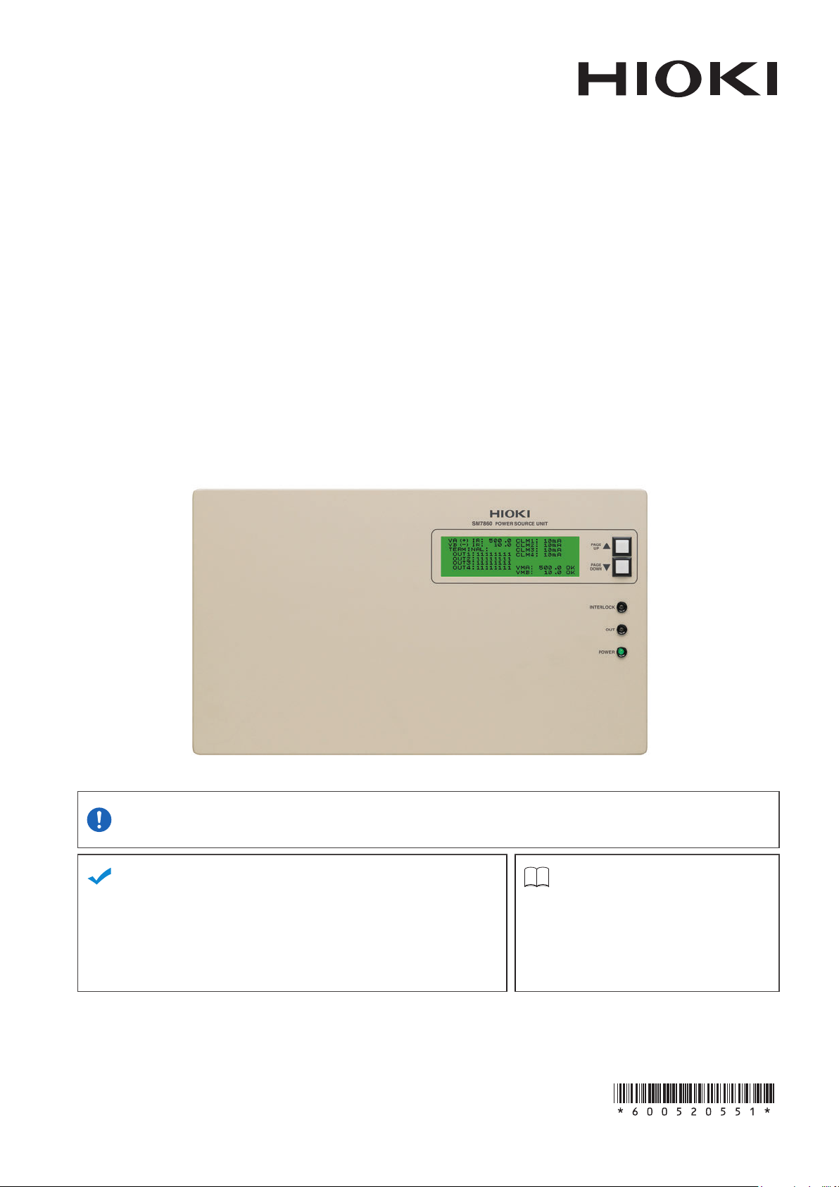
Instruction Manual
POWER SOURCE UNIT
Be sure to read this manual
before using the device
When using the device for the rst time Troubleshooting
Part Names and Functions
Screen Conguration
Installation and Connection Procedures
July 2018 Revised edition 1
SM7860J961-01 18-07H
p.
p.
p.
10
13
15
Safety Information
Troubleshooting
Error Display
p.
p.
p.
4
53
55
EN


Contents
Introduction
Notation
Verifying Package Contents
Safety Information
Operating Precautions
........................................................1
..............................................................2
............................3
............................................4
.....................................4
1 Overview 9
1.1 Product Overview and Features
1.2 Part Names and Functions
1.3 ScreenConguration
...........................13
...........9
.................10
2 Preparation and Supply
Power
2.1 Installation and Connection
Procedures
2.2 Connecting the Power Cord
2.3 Connecting the Device to the
Measuring Instrument
2.4 Inspection Before Operation
2.5 Turn ON/OFF the power
2.6 Operating Conditions Setting
2.7 Output Setting for the Device
Interlocked
15
............................................15
................16
..........................17
...............18
......................19
..............20
.............................................21
4 External Control 37
4.1 EXT I/O Connector and Signals
Connector Type and Signal Pinouts
Signal Functions
4.2 Timing Chart
4.3 Internal Circuitry
.......................................39
..........................................40
....................................44
.........37
...........38
5 Specications 45
5.1 GeneralSpecications
5.2 BasicSpecications
Graph description and operating
precautions
...............................................50
5.3 Input / Output Functions
.........................45
.............................46
......................52
6 Maintenance and Service 53
6.1 Troubleshooting
6.2 Error Display
6.3 Repairs, Inspections, and Cleaning
6.4 Replacing the Power Fuse
Warranty Certicate
....................................53
.........................................55
...55
..................56
3 Changing the Interface 23
3.1 Overview and Features of the
Interfaces
3.2 InterfaceSpecications
3.3 Connecting the Interface
Using the GP-IB Interface
Using the RS-232C Interface
3.4 ConguringtheCommunications
Protocol
ConguringGP-IBInterface
Communications
ConguringRS-232CInterface
Communications
3.5 Communication Method
Status Byte Register
Event Register
Error Register
3.6 Message List
3.7 ListenerSpecicationPrecautions
Input buffer size
Reading from the output buffer
...............................................23
.......................24
.....................26
GP-IB
..................................................27
GP-IB
...........................27
RS-232C
.................................30
..........................................31
...........................................33
.........................................34
........................................36
..............26
RS-232C
.......................28
.......................28
..................36
.....26
.....36
SM7860J961-01
i

Contents
ii
Introduction
Introduction
Thank you for purchasing the Hioki Model SM7860 series Power Source Unit.
To obtain maximum performance from the device over the long term, be sure to read this manual carefully
and keep it handy for future reference.
Target audience
This manual has been written for use by individuals who use the product in question or who teach
others to do so. It is assumed that the reader possesses basic electrical knowledge (equivalent to that of
someone who graduated from the electrical program at a technical high school).
Finding the product’s model number
You can nd the model number on the rear of the device.
Model Overview Supply voltage
SM7860-51 500 V × 32 channels 100 V to 110 V
SM7860-52 1000 V × 32 channels 100 V to 110 V
SM7860-53 500 V × 16 channels, −500 V × 16 channels 100 V to 110 V
SM7860-54 1000 V × 16 channels, −1000 V × 16 channels 100 V to 110 V
SM7860-55 500 V × 8 channels, −500 V × 8 channels, discharge × 16 channels 100 V to 110 V
SM7860-56 1000 V × 16 channels, −1000 V × 16 channels, discharge × 16 channels 100 V to 110 V
SM7860-57 10 V × 24 channels, discharge × 8 channels 100 V to 110 V
SM7860-58 500 V × 24 channels, discharge × 8 channels 100 V to 110 V
SM7860-61 500 V × 32 channels 220 V
SM7860-62 1000 V × 32 channels 220 V
SM7860-63 500 V × 16 channels, −500 V × 16 channels 220 V
SM7860-64 1000 V × 16 channels, −1000 V × 16 channels 220 V
SM7860-65 500 V × 8 channels, −500 V × 8 channels, discharge × 16 channels 220 V
SM7860-66 1000 V × 16 channels, −1000 V × 16 channels, discharge × 16 channels 220 V
SM7860-67 10 V × 24 channels, discharge × 8 channels 220 V
SM7860-68 500 V × 24 channels, discharge × 8 channels 220 V
1
Notation
Notation
Concerning Safety
In this document, the risk seriousness and the hazard levels are classied as follows.
DANGER
WARNING
CAUTION
IMPORTANT
Imminent risk of operator death or serious injury
Potential for operator death or serious injury
Potential for minor operator injury or device damage or malfunction
Indicates information related to the operation of the device or maintenance tasks
with which the operators must be fully familiar.
Prohibited actions
Actions that must be performed
Symbols Afxed to the Device
Precaution or hazard (See “Operating Precautions”.)
ON side of the power switch
OFF side of the power switch
AC (alternating current)
Grounding terminal
Others
*
p.
[ ]
ON
Additional information is presented below.
Indicates the location of reference information.
Key names are indicated in brackets.
Names and keys on the screen are shown in boldface.
Accuracy
We dene measurement tolerances in terms of f.s. (full scale), rdg. (reading), and dgt. (digit) values, with
the following meanings:
f.s. (maximum display value)
f.s.
rdg.
The maximum displayable value. This is usually the name of the currently
selected range.
rdg. (reading or displayed value)
The value currently being measured and indicated on the measuring device.
dgt. (resolution)
dgt.
The smallest displayable unit on a digital measuring device, i.e., the input value
that causes the digital display to show a “1” as the least-signicant digit.
2
Verifying Package Contents
Verifying Package Contents
When you receive the device, inspect it carefully to ensure that no damage occurred during shipping.
In particular, check the accessories, panel switches, and connectors. If damage is evident, or if it fails to
operate according to the specications, contact your authorized Hioki distributor or reseller.
Device and Accessories
Conrm that you have received the following items:
Model SM7860 series Power Source Unit
Power cord
Instruction Manual (This document)
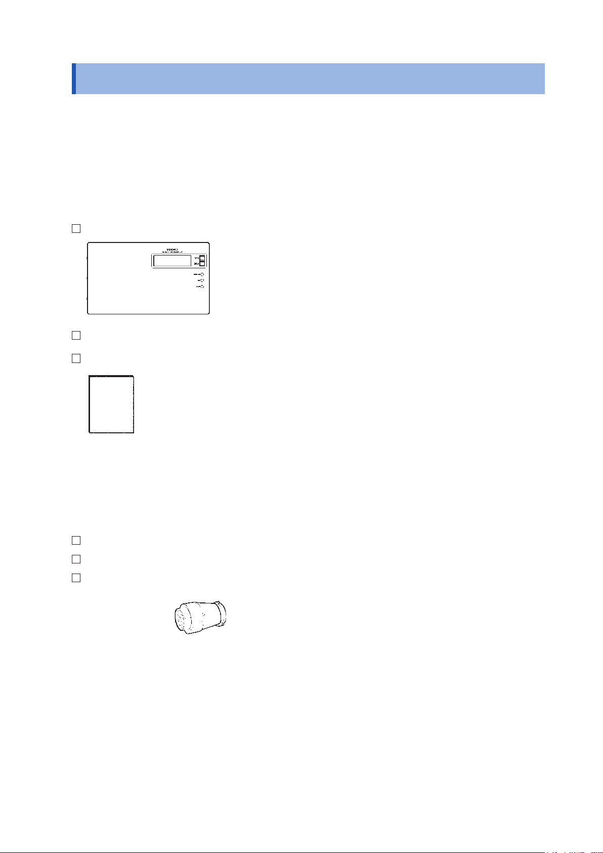
Options
The following options are available for the device. Contact your authorized Hioki distributor or reseller
when ordering.
Model 9637 RS-232C Cable (9pin-9pin/1.8 m) Cross
Model 9151-02 GP-IB Connector Cable 2 m
Model L2221 Connector Voltage output
3
Safety Information
Safety Information
Before using the device, be certain to carefully read the following safety notes.
DANGER
Mishandling during use could result in injury or death, as well as damage to the
device. Be certain that you understand the instructions and precautions in the
manual before use.
WARNING
• With regard to the electricity supply, there are risks of an electric shock,
heat generation, re, and arc ash due to a short-circuit. Individuals using
an electrical measuring device for the rst time should be supervised by a
technician who has experience in electrical measurement.
• Protective gear
This device is measured on a live line. To prevent an electric shock, use
appropriate protective insulation and adhere to applicable laws and regulations.
Operating Precautions
Follow these precautions to ensure safe operation and to obtain the full benets of the various functions.
Checks before use
DANGER
If the connection cord or the device is damaged, there is a risk of an electric
shock. Perform the following inspection before using the device:
• Check that the coatings of the connection cords are neither ripped nor torn and
that no metal parts are exposed. Using the device under such conditions could
result in an electric shock. Replace the connection cords with those specied
by our company.
• Verify that the device operates normally to ensure that no damage occurred
during storage or shipping. If you nd any damage, contact your authorized
Hioki distributor or reseller.
WARNING
To prevent an electric shock, conrm that the white or red portion (insulation
layer) inside the cable is not exposed. If a color inside the cable is exposed, do
not use the cable.
4
Installing the device
• Ventilation holes for heat radiation are provided on the side and rear panels of
the device. Leave sufcient space around the ventilation holes and install the
device with the holes unobstructed. Installation of the device with the ventilation
holes obstructed may cause a malfunction or a re.
• Unplugging the power cord kills power to the device. Be sure to provide enough
unobstructed space to unplug the power cord immediately in an emergency.
Installing the device in inappropriate locations may cause a malfunction of device
or may give rise to an accident. Avoid the following locations:
• Exposed to direct sunlight or high temperature
• Exposed to corrosive or combustible gases
• Exposed to a strong electromagnetic eld or electrostatic charge
• Near induction heating systems (such as high-frequency induction heating
systems and IH cooking equipment)
• Susceptible to vibration
• Exposed to water, oil, chemicals, or solvents
• Exposed to high humidity or condensation
• Exposed to high quantities of dust particles
Operating Precautions
WARNING
CAUTION
Failure to observe the following precaution may result in bodily injury.
• The device weighs approx. 47 kg (Model SM7860-57 and SM7860-67: approx. 34 kg).
It should be moved by at least two people, who should grip it using the handles on the
left and right sides. The center of gravity is located on the front side of the device.
• The device is heavy. When transporting it, follow your company’s workplace safety
standards to assure safety (for example, by wearing non-slip gloves and protective
footwear).
Do not place the device on an unstable table or inclined place. Dropping or knocking
down the device can cause injury or damage to the device.
5
Operating Precautions
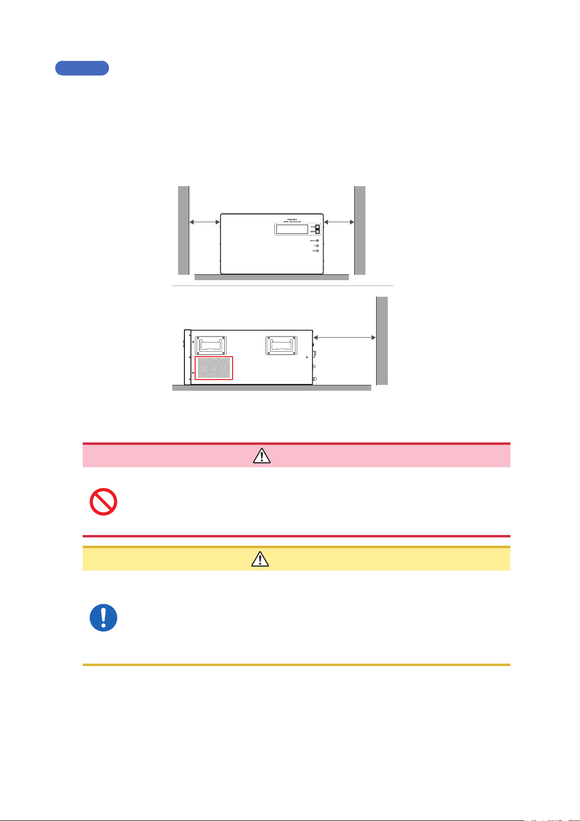
Installing
Prolonged operation in hot temperatures will shorten the device’s service life. Keep the ambient temperature
as low as possible.
• Avoid obstructing the ventilation holes.
• To prevent overheating, be sure to leave the specied clearances around the device.
• When rack-mounting the device, fans must be installed above or on top of the rack to ensure proper
ventilation. Be sure that the rack is adequately ventilated so that the internal temperature remains at or
below 40°C.
Handling the Device
• Do not use the device with circuits that exceed its ratings or specications.
Doing so may damage the device or cause it to become hot, resulting in a bodily
injury.
• Do not short-circuit two wires to be measured by bringing the cable into contact
with them. Arcs or such grave accidents are likely to occur.
50 mm or more
Prevent from
blocking
50 mm or more
100 mm or more
DANGER
CAUTION
Failure to observe the following precaution may result in bodily injury.
• The device weighs approx. 47 kg (Model SM7860-57 and SM7860-67: approx. 34 kg).
It should be moved by at least two people, who should grip it using the handles on the
left and right sides. The center of gravity is located on the front side of the device.
• The device is heavy. When transporting it, follow your company’s workplace safety
standards to assure safety (for example, by wearing non-slip gloves and protective
footwear).
6
Handling the Cords
If the insulation on a cord melts, the metal conductor may be exposed. Do not use
any cord whose metal conductor is exposed. Doing so could result in an electric
shock, burn, or other hazards.
To avoid damaging the power cord, grasp the plug, not the cord, when unplugging it
from the outlet or device.
To prevent cord damage, do not step on cords or pinch them between other objects. Do
not bend or pull on cables at their base.
IMPORTANT
Use only the specied connection cords. Use of any cable not specied by our company may
result in incorrect measurements due to poor connection or other reasons.
Operating Precautions
WARNING
CAUTION
To ensure accurate measurements
• Warm up the device an hour or more before use.
• The device should be calibrated once a year.
Transporting Precautions
• To ensure safe handling, when transporting the device, please use the original box and packing
materials, but do not use if the box is damaged or warped, or if the packing materials are in poor
condition or incomplete.
• When packing the device, make sure to disconnect power supply cords from the main device.
• When transporting, avoid dropping or other excessive impacts.
7

Operating Precautions
8

1
Overview
1.1 Product Overview and Features
The SM7860 series Power Source Unit is a power source designed for use with the SM7420 Super
Megohm Meter and SM7810‑20 Super MΩ HiTester. When used in conjunction with the SM7420 or
SM7810‑20, the SM7860 serves as an ideal power source for automatic testing and measurement of
capacitors.
Positive- and negative-polarity output / Multi-channel output
• The device supports multichannel systems with up to 32 channels.
• The output voltage can be set separately for two circuits, each consisting of 8 or 16 channels.
• The device provides both positive‑ and negative‑polarity power sources.
• It can be used to create an optimal testing line with the minimum necessary number of power sources.
Independent on/off output switching and current limitations for all channels
• Since each channel has its own output on/off switch, it is possible to control voltage application
without an external circuit (allowing charging and discharging).
• Use of semiconductor switches eliminates the need for maintenance.
• Ability to limit current for individual channels means the measurement of other channels won’t be
affected when a target workpiece has a short.
Variable output current limit value
• 500 V output model: The output current limit can be set as desired from 2 mA per channel to 50 mA
per channel.
• 1000 V output model: The output current limit can be set as desired from 2 mA per channel to 10 mA
per channel.
1000 V output voltage model
• The line includes a model that can generate output of up to ±1000 V.
High-current output at 50 mA/channel*
• The device can quickly charge high‑capacity MLCC (multi‑layer ceramic capacitor). Number of
charges can be reduced.
* For the 1000 V model, limited to 10 mA/channel.
Standard interfaces
• Devices ship standard with EXT. I/O, GP‑IB, and RS‑232C interfaces for sequencing. Interfaces are
used to congure and power the device.
Interlock function
• Since the device outputs measurement and charging voltages when measurement starts, erroneous
operation poses the risk of electric shock. An interlock function is used to ensure safe measurement.
Settings can be congured by sending signals via the device’s external I/O interface.
9
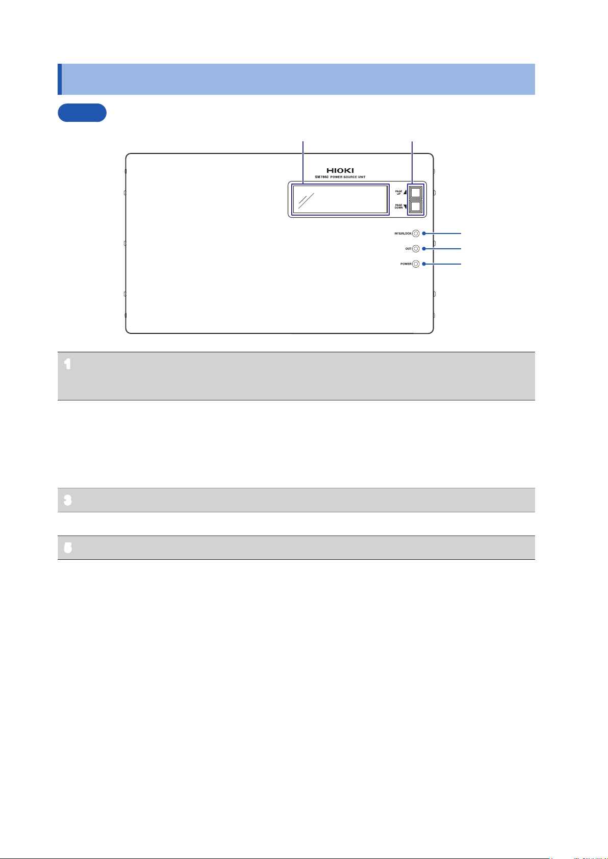
Part Names and Functions
1 2
3
4
5
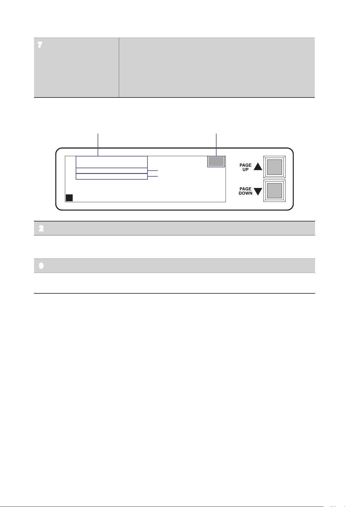
1.2 Part Names and Functions
Front
Display (LCD) The screen uses a 2‑page layout to display setting values
1
and setting status information.
Refer to “1.3 Screen Conguration” (p. 13)
Scroll keys
2
[PAGE UP▲], [PAGE DOWN▼]
Interlock indicator (INTERLOCK) Lights up when the interlock is on.
3
Voltage output indicator (OUT) Lights up when a voltage is being output.
4
Power indicator (POWER) Lights up when the device is on.
5
• Use to scroll the display (LCD).
Refer to “1.3 Screen Conguration” (p. 13)
• Used to assign the GP-IP address and to congure the
output setting for the device interlocked.
Refer to “Conguring GP-IB Interface Communications
GP-IB” (p. 27)
10
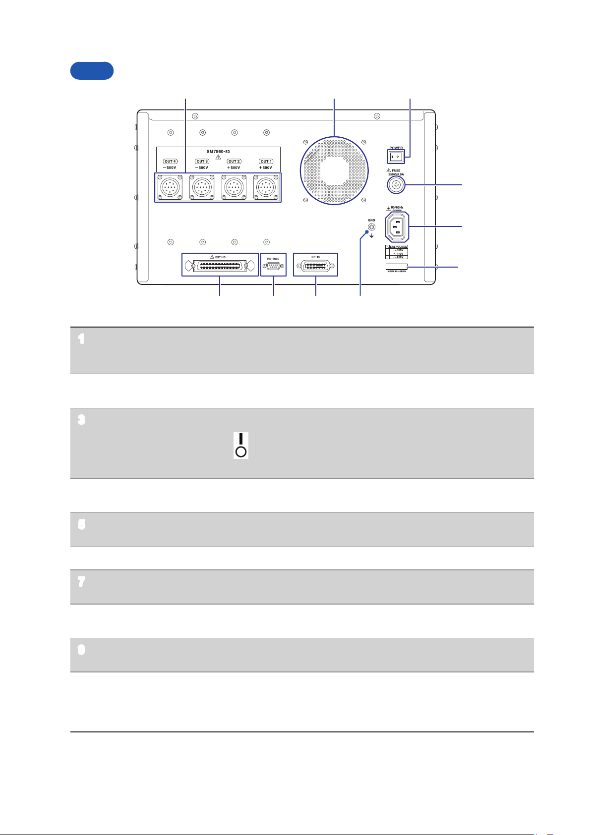
Rear
1 32
4
5
6 789
10
Part Names and Functions
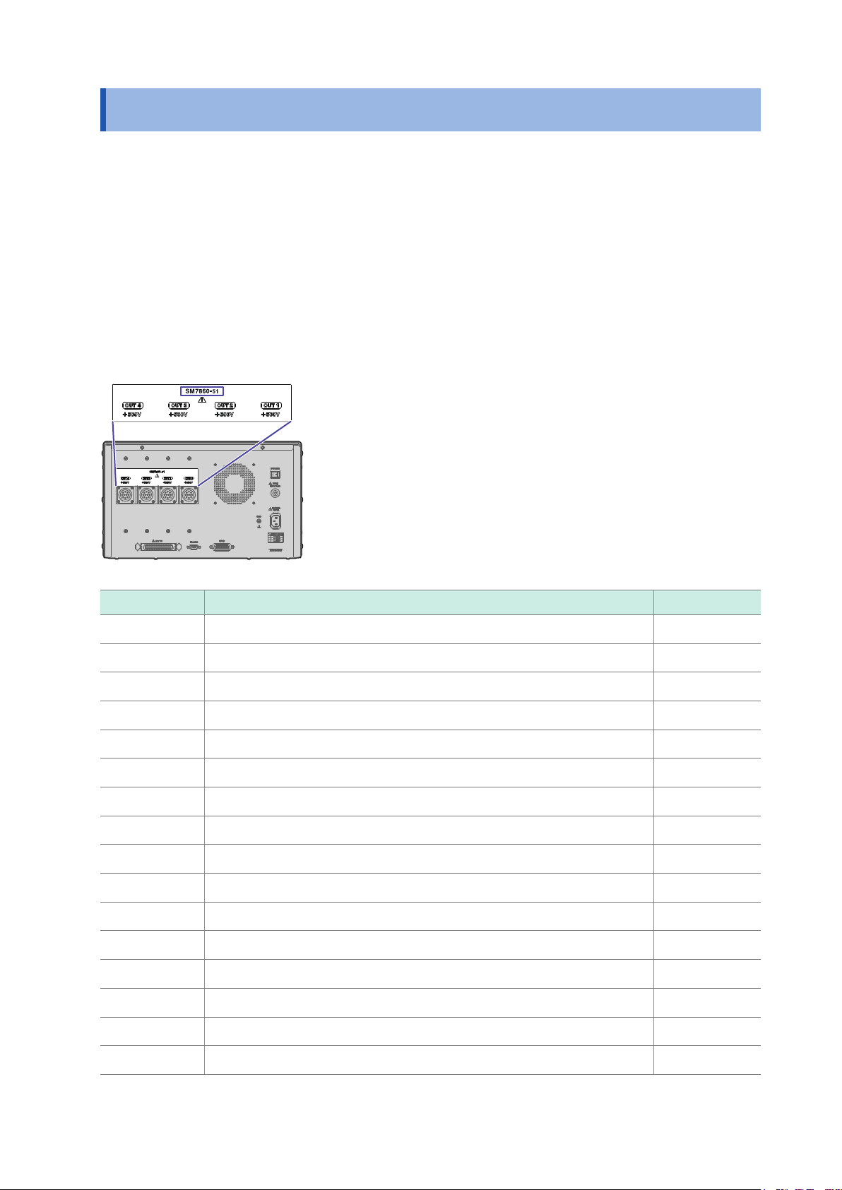
Voltage output terminal Voltage is output. Connect the optional Model L2221 Connector.
1
Ventilation holes Keep clear of obstructions.
2
Power switch (POWER) Turns the device on and off.
3
Fuse holder (FUSE) Fuse can be replaced.
4
Power inlet Connect the supplied power cord.
5
GND terminal Serves as the ground terminal. Connects to the device’s enclosure.
6
GP‑IB connector Connect to a PC when using the GP‑IB interface.
7
RS‑232C connector Connect to a PC when using the RS‑232C interface.
8
Refer to “2.3 Connecting the Device to the Measuring Instrument”
(p. 17)
Refer to “Installing” (p. 6)
: Power ON
: Power OFF
Refer to “2.5 Turn ON/OFF the power” (p. 19)
Refer to “6.4 Replacing the Power Fuse” (p. 56)
Refer to “2.2 Connecting the Power Cord” (p. 16)
Refer to “Using the GP-IB Interface GP-IB” (p. 26)
Refer to “Using the RS-232C Interface RS-232C” (p. 26)
EXT I/O connector The EXT I/O connector can be used to control the device.
9
Refer to “4 External Control” (p. 37)
Serial number The serial number consists of 9 digits. The rst two (from the left)
10
indicate the year of manufacture, and the next two indicate the
month of manufacture.
Required for production control. Do not peel off the label.
11
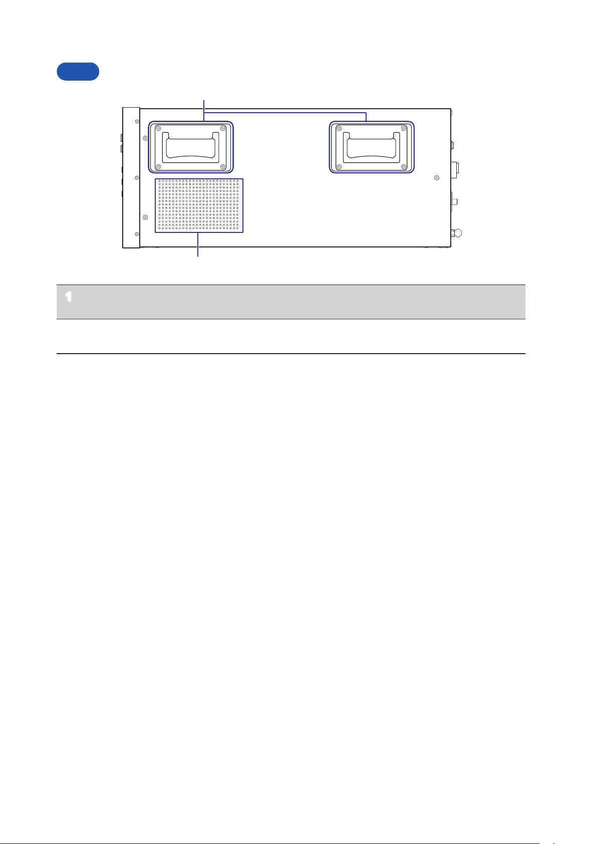
Part Names and Functions
1
2
Side
Handle (total of 4, located on the
1
left and right sides of the device)
Ventilation holes Keep clear of obstructions.
2
It should be moved by at least two people, who should grip
it using the handles on the left and right sides.
Refer to “Installing” (p. 6)
12
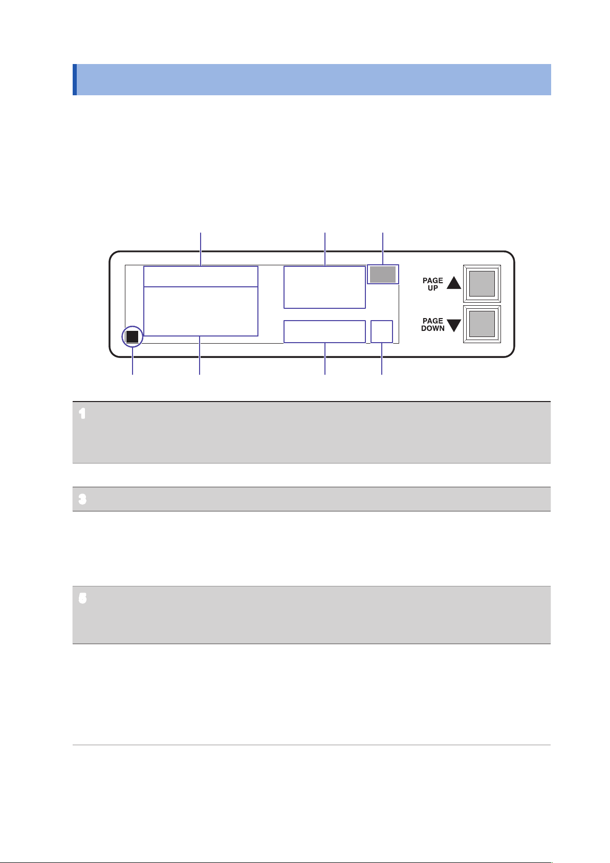
Screen Conguration
1
3 4 5 6
27
1.3 Screen Conguration
The display (LCD) consists of two display pages (Screen P1, Screen P2).
• Screen P1 is displayed when the device is turned on.
• The display pages can be scrolled using the scroll keys ([PAGE UP▲], [PAGE DOWN▼]) to the right of
the screen.
• You can select a display page directly by sending a “
interface. Refer to “3.6 Message List” (p. 34)
Screen P1: Displays output voltage settings
P1
PAG
” command from the GP-IB or RS-232C
VA (+) IR:1000.0
VB (+) IR: 250.0
TERMINAL:
OUT1:11100000
OUT2:11100000
OUT3:11100000
OUT4:11100000
L
Output voltage setting VA : Displays the power supply A circuit voltage setting.
1
VB : Displays the power supply B circuit voltage setting.
( Display example: VA (+) IR: 1000.0
Indicates that the power source’s A circuit is set to 1000.0 V.)
Temperature error display When a temperature error is detected, TEMP blinks.
2
Key lock display When the keys are locked, L is displayed.
3
Terminal output setting
4
state
Displays rows 1 through 8 of OUTn (where n indicates a value from 1
to 4), from left to right.
The setting is 0 or 1.
0 : High‑impedance
1 : ON
CLM1: 10mA
CLM2: 10mA
CLM3: 10mA
CLM4: 10mA
VMA: 1000.0
VMB: 250.0
TEMP
TEMP
OK
OK
Monitor voltage value VMA : Voltage monitor value for the power supply A circuit.
5
VMB : Voltage monitor value for the power supply B circuit.
The zero decimal point’s position is xed using zero suppression.
Voltage error alarm results
6
OK: The monitor voltage (5) error relative to the output voltage setting
(1) falls within the normal range relative to the voltage error alarm
setting (8, p. 14).
NG: The monitor voltage (5) error relative to the output voltage setting
(1) indicates an error relative to the voltage error alarm setting (8,
p. 14).
13
Screen Conguration
8
2
P2
Output current limit value CLM1 : OUT1 output current limit value setting display
7
CLM2 : OUT2 output current limit value setting display
CLM3 : OUT3 output current limit value setting display
CLM4 : OUT4 output current limit value setting display
The digit following CLM corresponds to OUT1 to 4.
( Display example: CLM1: 10mA
Indicates that the current output from OUT1 is limited to 10 mA.)
Screen P2: Displays alarms, the GP-IP address, and output setting for the device interlocked.
VA ALARM : 19
VB ALARM : 19
GPIB ADDR: 1
ILOCK DCHG: OFF
9
10
TEMP
TEMP
L
Temperature error display When a temperature error is detected, TEMP blinks.
2
Voltage error alarm setting VA ALARM : Power supply A circuit voltage error alarm setting ± (%)
8
VB ALARM : Power supply B circuit voltage error alarm setting ± (%)
GP‑IB address Refer to “Using the GP-IB Interface GP-IB” (p. 26)
9
Output setting for the
10
device interlocked
Refer to “2.7 Output Setting for the Device Interlocked” (p. 21)
14

2
Preparation and Supply Power
2.1 Installation and Connection Procedures
Be sure to read the “Operating Precautions” (p. 4) before installing and connecting the device.
3
4
6
Front Rear
Install the device. (p. 5)
1
Connect the power cord. (p. 16)
2
Connect the device to the measuring instrument. (p. 17)
3
Connect the external interface.
4
• Using the GP-IB or RS-232C interface (p. 23)
• Using the EXT I/O (p. 37)
Complete the pre-use inspection. (p. 18)
5
Be sure to inspect the device prior to use.
2
Turn the power on. (p. 19)
6
Make device settings. (p. 20)
7
(via the external interface)
Activate the power source.
8
15

Connecting the Power Cord
2.2 Connecting the Power Cord
WARNING
• Before turning the device on, make sure the supply voltage matches that indicated
on its power connector. Connection to an improper supply voltage may damage the
device and present an electrical hazard.
• To prevent an electric shock and to maintain the safety specications of this device,
connect the power cord provided only to an outlet.
• Before using the device, make sure that the insulation on the power cord is
undamaged and that no bare conductors are improperly exposed. Using the device in
such conditions could cause an electric shock, so replace the power cord with those
specied by our company.
CAUTION
To avoid damaging the power cord, grasp the plug, not the cord, when unplugging it from the
outlet or device.
Turn off the power before disconnecting the power cord.
Connection Method
1
Power inlet
2
Conrm that the device is turned off.
1
Conrm that the supply voltage
2
matches the device, and connect the
power cord to the power inlet on the
device.
Plug the power cord into the outlet.
3
This completes the process of
connecting the power cord.
16

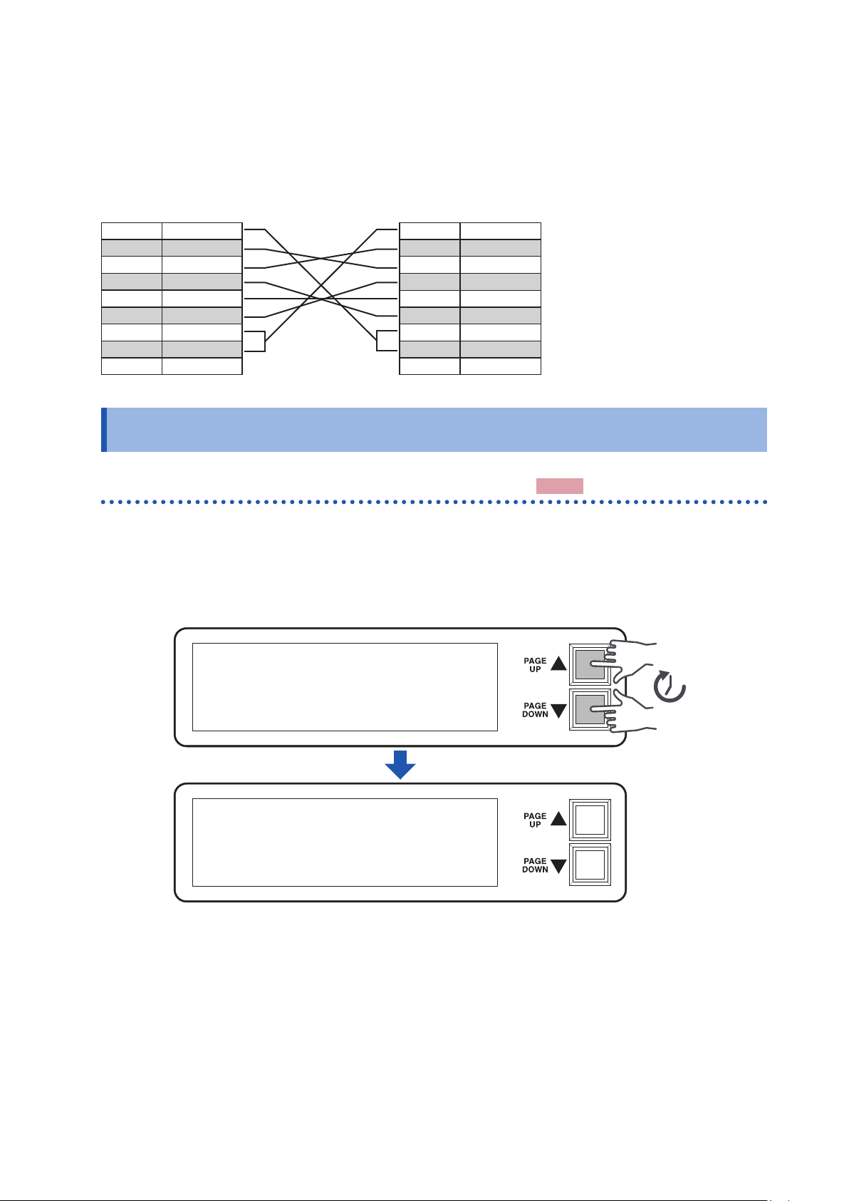
Connecting the Device to the Measuring Instrument
2.3 Connecting the Device to the Measuring Instrument
WARNING
To prevent an electric shock or damage to the equipment, always observe the following
precautions when connecting to voltage output terminal:
• Always turn off the device and any devices to be connected before connecting the
voltage output connectors.
CAUTION
To avoid damage to the device, be sure to observe the following precautions:
• Do not connect the device to a load with a charge in excess of the output voltage range.
• Do not connect the device to a load with a charge that has the opposite polarity of the output
voltage range.
• Do not connect the device to a load that has a charge when the device is turned off.
Connection Method
Conrm that the device is turned off.
1
Connect model L2221 Connector*1
OUT1
2
(optional) to the voltage output
terminal on the rear of the device.
This completes the process of
connecting the device to the
measuring instrument.
1
OUT2*
Circuit A
OUT3
Circuit B
OUT4*
Circuit B
1
2
*1: Refer to “Voltage output pin assignment specications” described below to modify the L2221 to
connect measurement targets.
Voltage output pin assignment
specications
3
2
1
Pin No.
1 CH1 CH1 CH1 CH1
2 CH2 CH2 CH2 CH2
3 CH3 CH3 CH3 CH3
Circuit A
2
7
10 8
9
456
4 CH4 CH4 CH4 CH4
5 CH5 CH5 CH5 CH5
6 CH6 CH6 CH6 CH6
7 CH7 CH7 CH7 CH7
8 CH8 CH8 CH8 CH8
9 NC NC NC NC
10 COM COM COM COM
*1: On the SM7860-55, -56, -65, and -66, serves as the discharging terminal.
*2: On the SM7860-55, -56, -57, -58, -65, -66, -67, and -68, serves as the
discharging terminal.
17

Inspection Before Operation
2.4 Inspection Before Operation
Verify that the device operates normally to ensure that no damage occurred during storage or shipping. If
you nd any damage, contact your authorized Hioki distributor or reseller.
Inspection of peripheral devices
• Is the power cord insulation torn, or
is any metal exposed?
• Is the connection cord insulation
torn, or is any metal exposed?
Not exposed
Inspection of device
Is there any damage on the device?
No
Does the supply voltage of your
power source match the supply
voltage indicated on the power
source inlet on the rear of the
device?
Exposed
Do not use them if they are damaged
because it may cause an electric shock.
(Replace with a new cord.)
Yes
If any, request repair.
No
Use of a supply voltage outside the
specied range may damage the device
or cause an electric shock.
Yes
The inspection is complete.
Please read the “Operating Precautions” (p. 4) before use.
18

2.5 Turn ON/OFF the power
WARNING
Before turning the device on, make sure the supply voltage matches that indicated on
its power connector. Connection to an improper supply voltage may damage the device
and present an electrical hazard.
When turning the device on and off, do not touch the voltage output terminals. Doing so
may cause an electric shock.
CAUTION
When turning the device on and off, do not connect a load to the voltage output terminals.
Turning the device on or off with a load connected may damage the load.
Turn on the power
Turn ON/OFF the power
Turn on the power switch.
The power indicator and display (LCD) on
the front of the device will light up.
Turn off the power
Before Starting Measurement
To obtain precise measurements, provide
about an hour warm-up after turning on the
power.
Turn off the power switch.
19

Operating Conditions Setting
2.6 Operating Conditions Setting
This section describes how to set the operating conditions according to the manner in which the device is
to be used. Settings are congured via either of the device’s external interfaces:
Refer to “3 Changing the Interface” (p. 23)
The device cannot be congured directly in a standalone manner.
Setting function Description of operation and settings Reference
Output voltage
Voltage error alarm
LCD display mode
Sets the output voltage.
Setup ranges: 1.0 V to 1000.0 V (0.1 V resolution)
Generates an alarm when the monitor voltage error relative to the output
voltage setting falls outside the set value range.
Setup ranges: ±2 to ±19% (1% resolution)
Turns the LCD display on and off.
OFF/ ON
p. 34
p. 34
p. 35
20

Output Setting for the Device Interlocked
3 s
2.7 Output Setting for the Device Interlocked
This section describes how to choose between an impedance state and a discharging state for the output
with the device interlocked.
This setting remains the same even after the device is initialized.
ILOCK DCHG: OFF High-impedance state (Default)
ILOCK DCHG: ON Discharging state
Press and hold both of the scroll keys ([PAGE UP▲] and [PAGE DOWN▼]) on the right of
1
the screen simultaneously for approx. 3 s.
(The address can be set from the P1 or P2 screen.)
The GP-IB-address assigning screen is displayed.
VA (+) IR:1000.0
VB (+) IR: 250.0
TERMINAL:
OUT1:11100000
OUT2:11100000
OUT3:11100000
OUT4:11100000
GPIB ADDR: 1
Press and hold both the scroll keys ([PAGE UP▲] and [PAGE DOWN▼]) again
2
CLM1: 10mA
CLM2: 10mA
CLM3: 10mA
CLM4: 10mA
VMA: 1000.0 OK
VMB: 250.0 OK
simultaneously for 3 s.
The setting screen for the output setting for the device interlocked is displayed.
Press either of the scroll keys ([PAGE UP▲] or [PAGE DOWN▼]).
3
The output state is switched.
ILOCK DCHG: OFF
ILOCK DCHG: ON
Turn off the device once you have nished conguring the settings.
4
21

Output Setting for the Device Interlocked
22

3
The mark shown below indicates that the following instructions are specic to the RS-232C or the GP-IB
interface. Instructions without these symbols are for both the RS-232C and the GP-IB interface.
Changing the Interface
GP-IB
RS-232C
Before communicating
When connecting a GP-IB or RS-232 cable, be sure to secure the connector in place with screws or other
appropriate hardware.
When issuing commands that contain data, make sure that the data is provided in the specied format.
1
2
3
: GP-IB interface only
: RS-232C interface only
Connect the cable. (p. 26)
Connect the device and controller (PC etc.) with a GP-IB connection cable or RS-232C interface
cable.
Set the communications protocol.
GP-IB
RS-232C
(p. 28)
Set the transmission format.
Enter a GP-IB address. (p. 27)
Set the device to the same communications protocol as the controller (PC etc.).
3.1 Overview and Features of the Interfaces
The device provides standard communication functionality in the form of GP-IB and RS-232C interfaces,
both of which can be used to control the device remotely and to transfer data.
GP-IB
This device is designed with reference to the following standard:
Reference standard IEEE 488.1-1987
23

Interface Specications
3.2 Interface Specications
Precautions
RS-232C and GP-IB communications cannot be used simultaneously.
(1) GP-IB Specications
• Electrical machinery specications: IEEE std. 488.1-1987 compliant
• Address setting: Can be set to talker/listener addresses 1 to 30.
Interface Functions
SH1 Source handshake functions (all)
AH1 Acceptor handshake functions (all)
T6 Basic talker functions
L4 Basic listener functions
SR1 Service request functions (all)
RL1 Remote/Local functions (all)
GP-IB
Serial poll function
Talk-only mode
The talker cancel function with MLA (My Listen Address)
Listen-only mode
The listener cancel function with MTA (My Talk Address)
: Available,
–
: Unavailable
–
–
PP0 Parallel poll function –
DC1 Device clear functions (all)
DT1 Device trigger functions (all)
C0 Controller function –
E2 Tri-state output
Operating code: ASCII codes
24

Interface Specications
(2) RS-232C Specications
Transfer method Communication method: Full duplex
Transmission rate 38400 bps xed
Data bit length 8 bits
Stop bit 1 bit
Parity bit None
Delimiter Transmit: CR+LF
Flow control No X ow control, no hardware ow control
Protocol TTY
Electrical
specication
Connector Male 9-pin D-sub, with #4-40 attachment screws,
RS-232C
Synchronization method: Asynchronous
Receive: CR, CR+LF
Input voltage level 5 V to 15 V: ON
−15 V to −5 V: OFF
Output voltage level +5 V or more: ON
−5 V or less: OFF
The I/O connector is a DTE (Data Terminal Equipment) conguration
Recommended cable: Model 9637 RS-232C Cable (9 pin-9 pin/1.8 m)
Refer to “3.3 Connecting the Interface” (p. 26)
Operating code: ASCII codes
25

Connecting the Interface
6 7 8 9
3.3 Connecting the Interface
WARNING
• To avoid equipment failure, do not disconnect the communications cable while
communications are in progress.
• Use a common ground for both the device and the PC. Using different ground circuits
will result in a potential difference between the device’s ground and the PC’s ground.
If the communications cable is connected while such a potential difference exists, it
may result in equipment malfunction or failure.
• Before connecting or disconnecting any communications cable, always turn off the
device and the PC. Failure to do so could result in equipment malfunction or damage.
• After connecting the communications cable, tighten the screws on the connector securely.
Failure to secure the connector could result in equipment malfunction or damage.
CAUTION
To avoid damage to the device, do not short-circuit the terminal and do not input voltage to the
terminal.
Using the GP-IB Interface
Connect the GP-IB cable to the GP-IB connector.
Recommended cable: Model 9151-02 GP-IB Connector Cable (2 m)
Using the RS-232C Interface
Connect the RS-232C cable to the RS-232C connector.
Recommended cable: Model 9637 RS-232C Cable (9 pin-9 pin/1.8 m)
GP-IB
RS-232C
1 2 3 4 5
Pin No.
1 DCD CF CD Carrier detect Unused
2 RxD BB RD Receive data
3 TxD BA SD Transmit data
4 DTR CD ER Data terminal ready Unused
5 GND AB SG Signal ground
6 DSR CC DR Data set ready Unused
7 RTS CA RS Request to send Unused
8 CTS CB CS Clear to send Unused
9 RI CE CI Ring indicator Unused
Common name EIA JIS
Signal Name
Signal Remarks
26
Conguring the Communications Protocol
3 s
When connecting the device to a PC
Use a crossover cable with female 9-pin D-sub connectors.
Crossover Wiring
Female 9-pin D-sub Female 9-pin D-sub Recommended cable:
SM7860 side
Pin No. Pin No.
DCD 1
RxD 2 2 RxD
TxD 3 3 TxD
DTR 4 4 DTR
GND 5 5 GND
DSR 6 6 DSR
RTS 7 7 RTS
CTS 8 8 CTS
RI 9 9 RI
PC/AT Enhanced
Graphics Adapter
1 DCD
Model 9637 RS-232C Cable (9 pin9 pin/1.8 m)
3.4 Conguring the Communications Protocol
Conguring GP-IB Interface Communications
GP-IB
Setting the GP-IB address
Press and hold both of the scroll keys ([PAGE UP▲] and [PAGE DOWN▼]) on the right of
1
the screen simultaneously for approx. 3 s.
(The address can be set from the P1 or P2 screen.)
The setting screen is displayed.
VA (+) IR:1000.0
VB (+) IR: 250.0
TERMINAL:
OUT1:11100000
OUT2:11100000
OUT3:11100000
OUT4:11100000
GPIB ADDR: 1
CLM1: 10mA
CLM2: 10mA
CLM3: 10mA
CLM4: 10mA
VMA: 1000.0 OK
VMB: 250.0 OK
Press either of the scroll keys ([PAGE UP▲] or [PAGE DOWN▼]), set the desired address.
2
(Valid setting range: 1 to 30)
Turn off the device once you have nished conguring the settings.
3
27

Communication Method
Conguring RS-232C Interface Communications
Set the communications protocol on the controller (PC, etc.) to the same communications settings. For
more information about how to congure these settings, refer to the controller’s instruction manual or
other documentation.
Communication conditions
Baud rate 38400 bps
Parity none
Stop bit 1 bit
Data 8 bits
Flow control none
Remote switching requests
Send the
RS-232C interface communications will not be available until the
RMT
command from the RS-232C interface.
RMT
RS-232C
command is sent.
3.5 Communication Method
Various messages are supported for controlling the device through the interfaces.
Messages can be either program messages, sent from the controller such as PC to the device, or
response messages, sent from the device to the controller.
Program message
Controller
Response message
Message types are further categorized as follows.
Messages
When issuing commands that contain data, make certain that the data is provided in the specied format.
Program messages
Response message
Device (SM7860)
Command message
Query message
28

Program Messages
1. Command Messages and Query Messages
Command Messages
Commands that control the device, for example to congure settings or reset the device.
Query Messages
Requests for responses relating to results of operation or measurement, or the state of device settings.
Query commands end with a question (?) mark.
2. Message delimiter (terminator)
This device recognizes the following input message delimiters:
LF with CR+EOI
LF with EOI
CR with EOI
EOI
CR+LF
LF
Response Messages
1. Response Messages
When a query message is received, its syntax is checked and a response message is generated.
2. Message delimiter (terminator)
The following three response message delimiters can be specied with the “
LF (initial setting)
CR+LF
EOI
DLM
” command:
Communication Method
Separators
1. Message Unit Separator
Multiple message can be written in one line by separating them with semicolons “ ; ”.
2. Header Separator
In a message consisting of both a header and data, the header is separated from the data by a space (ASCII
code 20H).
3. Data Separator
In a message containing multiple data items, commas “,” are required to separate the data items from one
another.
Data Formats
Query messages use the formats outlined in the table below. The format is selected according to the command.
Response Messages and Parameter Data Types
Data type Description Example Remarks
NR1 Integer 0, 1, 2, 3 etc. Setting items, etc.
NR2 Fixed-point decimal number +12.345, 400.0 etc. Primarily setting values
NR3 Floating-point decimal number +1.234±50 etc. Primarily settings and measured values
ASCII ASCII string XXXXXXXXXXXXXXXX Primarily device IDs
29
Communication Method
Status Byte Register
RS-232C
GP-IB
: RS-232C reads the status bytes to nd out the status of the device.
: The device adopts the IEEE488.1-1987 dened status model for parts related to the serial
polling performed by the service request function. A trigger for generating a service request is
called an event.
Overview of Service Request Occurrence
Standard event register information
Output queue data information
Service request
occurrence
bit 7 bit 6 bit 5 bit 4 bit 3 bit 2 bit 1 bit 0
ERR
↓ ↑ ↓ ↓ ↓ ↓ ↓ ↓
& → Logical
↑ ↑ ↑ ↑ ↑ ↑ ↑ ↑
bit 7 bit 6 bit 5 bit 4 bit 3 bit 2 bit 1 bit 0
ERR × ESB MAV DSB unused unused unused
RQS
MSS
sum
ESB M AV DSB unused unused unused Status Byte Register (STB)
← & & & & & &
Each of these bits corresponds
to a specic event register
Service Request Enable Register
(SRER)
The Status Byte Register contains information about the event registers and the output queue. Required
items are selected from this information by masking with the Service Request Enable Register. When any
bit selected by the mask is set, bit 6 (MSS; the Master Summary Status) of the Status Byte Register is
also set, which generates an SRQ (Service Request) message and dispatches a service request.
For RS-232C, bit 4 (MAV message available) of the status byte register is not set.
30

Communication Method
Status Byte Register (STB)
A status byte register is an 8-bit register output from the unit to the controller during serial polling. If even
one of the status byte register bits enabled by the service request enable register changes from “0” to
“1” the MSS bit becomes 1. At the same time, the RQS bit also becomes “1” and a service request is
generated.
The RQS bit is always synchronized with the service request and only read and simultaneously cleared
upon being serial polled. The MSS bit is only read by an “
is cleared by a command such as a “
Bit 7 ERR Unrecoverable error
CLS
” command.
∗
STB?
” query and is not cleared until the event
∗
Bit 6 RQS
MSS
Bit 5 ESB Standard Event Status (logical sum) bit
Bit 4 M AV Message available
Bit 3 DSB Event Status (logical sum) bit
Bit 2 – Unused
Bit 1 – Unused
Bit 0 – Unused
Set to “1” when a service request is dispatched.
This is the logical sum of the other bits of the Status Byte Register.
This is logical sum of the Standard Event Status Register.
Indicates that a message is present in the output queue.
This is the logical sum of Event Status Register.
Service Request Enable Register (SRER)
This register masks the Status Byte Register. Setting a bit of this register to “1” enables the corresponding
bit of the Status Byte Register to be used.
Event Register
Standard Event Status Register (SESR)
A standard event status register is an 8-bit register.
If any bit in the Standard Event Status Register is set to “1” (after masking by the Standard Event Status
Enable Register), bit 5 (ESB) of the Status Byte Register is set to “1”.
Refer to “Standard Event Status Enable Register (SESER)” (p. 32)
The standard event status register is cleared at the following times:
• When a “
• When a “
CLS
” command is executed
∗
ERR?
” command is executed
• When the device power is cycled
31

Communication Method
Bit 7 PON Power-On Flag
Set to “1” when the power is turned on, or upon recovery from an outage.
Bit 6 URQ User Request
Unused
Bit 5 CME Command error (The command to the message terminator is ignored.)
This bit is set to “1” when a received command contains a syntactic or semantic error:
• Program header error
• Incorrect number of data parameters
• Invalid parameter format
• Received a command not supported by the device
Bit 4 EXE Execution Error
This bit is set to “1” when a received command cannot be executed for some reason.
• The specied data value is outside of the set range
• The specied setting data cannot be set
• Execution is prevented by some other operation being performed
Bit 3 DDE Device-Dependent Error
This bit is set to “1” when a command cannot be executed due to some reason
other than a command error, a query error or an execution error.
• When the command cannot be executed because there is an internal anomaly
Bit 2 QYE Query Error (the output queue is cleared)
This bit is set to “1” when a query error is detected by the controller of the output queue.
• When an attempt has been made to read an empty output queue (GP-IB only)
• When the data overows the output queue
• When data in the output queue has been lost
Bit 1 RQC Request Control
Unused
Bit 0 OPC Operation Complete
This bit is set to “1” in response to an “
• It indicates the completion of operations of all messages up to the “
∗
OPC
” command.
∗
OPC
” command
Standard Event Status Enable Register (SESER)
Setting any bit of the Standard Event Status Enable Register to “1” enables access to the corresponding
bit of the Standard Event Status Register.
Standard Event Status Register (SESR) and Standard Event Status Enable Register (SESER)
bit 6 bit 5 bit 4
SRQ
MSS Standard Event Status Register (SESR)
ESB MAV
↑
Logical
sum
bit 7 bit 6 bit 5 bit 4 bit 3 bit 2 bit 1 bit 0
PON URQ CME EXE DDE QYE RQC OPC
↓ ↓ ↓ ↓ ↓ ↓ ↓ ↓
← & & & & & & & &
↑ ↑ ↑ ↑ ↑ ↑ ↑ ↑
bit 7 bit 6 bit 5 bit 4 bit 3 bit 2 bit 1 bit 0
PON URQ CME EXE DDE QYE RQC OPC
Standard Event Status Enable Register (SESER)
32

Communication Method
Error Register
The Error Register, which consists of 8 bits, manages error information. The contents of this register
are aggregated in the CME, EXE, DDE, and QYE bits of the Standard Event Status Register (no mask
processing is performed).
Error register-related message are listed below.
CLS
∗
ERR?
bit 7 bit 6 bit 5 bit 4 bit 3 bit 2 bit 1 bit 0
– MLE HDE DFE DRE CNE ISE BDE Error Register
PON URQ CME EXE DDE QYE RQC OPC Standard Event Status Register
bit 7 bit 6 bit 5 bit 4 bit 3 bit 2 bit 1 bit 0
MLE: Message Length Error HDE: Header Error
DFE: Data Format Error DRE: Data Range Error
CNE: Can Not Execute ISE: Internal communication Error
BDE: Environment Backup was Damaged (RAM)
Clears the following registers:
• Status Byte Register
• Standard Event Status Register
• Error Register
Queries and clears the Error Register.
Error Register structure
Bit No. Name Event/status indicated by set bit
Bit 7 – Unused
Bit 6 MLE Message Length Error
Set when the message length exceeds the allowable range.
The bit is reset after the register is read.
Bit 5 HDE Message Header Error
Set when an unrecognizable message header is received.
The bit is reset after the register is read.
Bit 4 DFE Data Format Error
Set when the number of parameters exceeds the stipulated number or when there is an
unrecognizable parameter.
The bit is reset after the register is read.
Bit 3 DRE Data Range Error
Set when a parameter falls outside the stipulated range.
The bit is reset after the register is read.
Bit 2 CNE Unexecutable command
Set when an unexecutable command is received.
The bit is reset after the register is read.
Bit 1 ISE Internal communication error
Set when an internal communication error occurs.
The bit is reset after the register is read.
Bit 0 BDE Environment backup was damaged
Set when data stored in the device’s backup RAM is corrupted.
The bit is reset after the register is read.
33

Message List
3.6 Message List
RS-232C-only commands are indicated by
RS-232C
. When using the RS-232C interface to send
commands, include a uniform wait time of 100 ms (excluding the following exceptions).
Command Description Format
Communication condition
RMT
Delimiter
DLM
DLM?
Output voltage setting
VAI
VAI?
VBI
VBI?
Remote switching request
Talker delimiter specication
d1 (delimiter specication: 0 to 2)
0: LF<EOI> Default
1: CRLF<EOI>
2: <EOI>
Note: This setting reverts to its default when the device is powered on.
A combination CR+LF is used as the RS-232C delimiter for both
data transmission and reception.
Delimiter query
The contents of responses are the same as the settings.
Circuit A output voltage setting
d1: 1.0 V to 1000.0 V
Note: Set as an absolute value.
The valid setting range varies with the model.
Circuit A output voltage setting query
The contents of responses are the same as the settings.
Circuit B output voltage setting
d1: 1.0 V to 1000.0 V
Note: Set as an absolute value.
The valid setting range varies with the model.
Circuit B output voltage setting query
The contents of responses are the same as the settings.
Output voltage setting range by model
RS-232C
[Format] RMT
[Format] DLM d1
[Format]
[Response]
[Format] VAI d1
[Format]
[Response]
[Format] VBI d1
[Format]
[Response]
d1: NR1
format
DLM?
d1
d1: NR2
format
VAI?
d1
d1: NR2
format
VBI?
d1
Alarm setting
ARM
ARM?
Model Lower limit (V) Upper limit (V)
SM7860-51, -61 1.0 500.0
SM7860-52, -62 250.0 1000.0
SM7860-53, -63 1.0 500.0
SM7860-54, -64 250.0 1000.0
SM7860-55, -65 1.0 500.0
SM7860-56, -66 250.0 1000.0
SM7860-57, -67 1.0 10.0
SM7860-58, -68 1.0 500.0
Voltage error alarm setting
d1: 2% to 19%, Circuit A voltage error alarm setting
d2: 2% to 19%, Circuit B voltage error alarm setting
Note: d1 or d2 can be omitted.
Voltage error alarm setting query
The contents of responses are the same as the settings.
[Format] ARM d1,d2
ARM d1
ARM ,d2
[Format]
[Response]
ARM?
d1,d2
34
Command Description Format
Voltage monitor
VMA?
VMB?
Output current limit
CLM
CLM?
LCD display mode
LCD
LCD?
PAG
Error information
ERR?
Others
RST
∗
IDN?
∗
SAV
∗
RCL
∗
CLS
∗
SRE
∗
SRE?
∗
STB?
∗
ESE
∗
Circuit A power supply voltage monitor value query [Format]
[Response]
Circuit B power supply voltage monitor value query [Format]
[Response]
OUT1 to OUT4[mA]: 2 to 50 mA
Note: The valid setting range varies by model.
Current limit setting value query [Format]
LCD display mode setting
d1 (Display mode: 0 to 1)
0: OFF (Display off)
1: ON (Display on)
LCD display mode query
The contents of responses are the same as the settings.
LCD display page specication
d1 (Page number: 0 to 1)
0: Output voltage setting, monitor voltage value, channel-specic output
setting state
1: Alarm setting, GP-IB address
Error information query
d1 (Error information: 0 to 127)
Note: Error information is cleared when the response is output.
Resets the device
Restore all the settings to the factory default (except for the output setting
for the device interlocked).
Device operation will be stopped.
Hardware ID query
Returns the device’s hardware ID as the response.
d1 (HIOKI, SM7860-5x, 0, 01.00) or d1 (HIOKI, SM7860-6x, 0, 01.00)
Save environmental data (output voltage setting, current limit value, and
alarm setting)
d1 (Environmental data no.: 0 to 3)
Recall environmental data
(output voltage setting, current limit value, and alarm setting)
d1 (Environmental data no.: 0 to 3)
Clear status register [Format]∗CLS
Sets the service request enable register.
d1 (0 to 255)
Service request enable register query
d1 (0 to 63, 128 to 191)
Note: Bit 6 is not set by
Status byte register query
d1 (0 to 255)
Sets the standard event status enable register.
d1 (0 to 255)
∗
SRE
.
[Format] CLM
[Response]
[Format] LCD d1
[Format]
[Response]
[Format] PAG d1
[Format]
[Response]
[Format]∗RST
[Format]
[Response]
[Format]∗SAV d1
[Format]∗RCL d1
[Format]∗SRE d1
[Format]
[Response]
[Format]
[Response]
[Format]∗ESE d1
VMA?
d1: NR2
format
VMB?
d1: NR2
format
d1,d2,d3,d4
CLM?
d1 to d4:
NR1 format
d1: NR1
format
LCD?
d1: NR1
format
d1: NR1
format
ERR?
d1: NR1
format
∗
d1: String
d1: NR1
format
d1: NR1
format
d1: NR1
format
∗
d1: NR1
format
∗
d1: NR1
format
d1: NR1
format
Message List
IDN?
SRE?
STB?
35

Listener Specication Precautions
Command Description Format
ESE?
∗
ESR?
∗
OPC
∗
OPC?
∗
CNF
CNF?
KLC
KLC?
Standard event status enable register query
The contents of responses are the same as the settings.
Standard event status register query
d1 (0 to 255)
Sets the standard event status register’s OPC bit after all ongoing
operations have completed.
This command is used to detect the completion of commands that involve
time-consuming processing.
Returns the value “1” when all ongoing operations have completed.
d1: 1
Operating environment setting
d1 (Interlock control enable/disable: 0 to 1)
0: CONNECT (Enables interlock)
1: CUTOFF (Disables interlock) Default
Operating environment query
The contents of responses are the same as the settings.
Key lock setting
d1 (0 to 1)
0: Key lock off
1: Key lock on
Key lock query
d1 (0 to 1)
The contents of responses are the same as the settings.
[Format]
[Response]
[Format]
[Response]
[Format]∗OPC
[Format]
[Response]
[Format] CNF d1
[Format]
[Response]
[Format] KLC d1
[Format]
[Response]
ESE?
∗
d1: NR1
format
ESR?
∗
d1: NR1
format
OPC?
∗
d1: NR1
format
d1: NR1
format
CNF?
d1
d1: NR1
format
KLC?
d1: NR1
format
3.7 Listener Specication Precautions
Input buffer size
Multiple command messages can be transferred at once by joining them with message separators. Since
the device provides an 128-byte input buffer, the device is unable to receive message strings in excess
of 127 characters in length. In this case, the entire command will be ignored (discarded), and the Error
Register’s MLE (Message Length Error) bit will be set.
Reading from the output buffer
The output buffer uses a FIFO design, with older data being read rst. Consequently, the read value may
differ from the expected value under certain circumstances, for example if no response is acquired after
issuing a query. Additionally, the output buffer is 511 bytes in size. If data in excess of 511 bytes is written
to the buffer, it will be discarded, and the Error Register’s QYE (Query Error) bit will be set.
36
4
This chapter describes how to use the EXT I/O connector on the rear of the device to control the device.
External Control
4.1 EXT I/O Connector and Signals
WARNING
To prevent an electric shock or damage to the equipment, always observe the
following precautions when connecting the cables to EXT I/O connector:
• Always turn off the device and any devices to be connected before making
connections.
• During operation, a wire becoming dislocated and contacting another conductive
object can be serious hazard. Use bail locks to secure the EXT I/O connector.
• Ensure that devices and systems to be connected to the EXT I/O connector are
properly isolated from one another.
CAUTION
To avoid damage to the device, observe the following cautions:
• Do not apply voltage or current to the EXT I/O connector that exceeds their ratings.
• When driving relays, be sure to install diodes to absorb counter-electromotive force.
Refer to “Connector Type and Signal Pinouts” (p. 38)
37

EXT I/O Connector and Signals
Connector Type and Signal Pinouts
Connector: 57RE-40500-730B (50 pin: DDK)
26 27 28 29 30 31 32 33 34 35 36 37 38 39 40 41 42 43 44 45 46 47 48 49 50
1 2 3 4 5 6 7 8 9 10 11 12 13 14 15 16 17 18 19 20 21 22 23 24 25
EXT I/O connector
Pin No. Signal name I/O Pin No. Signal name I/O
1
2
3
4
5
6
7
8
9
10
11
12
13
14
15
COM
EXT_DCV2 (+24V)
OUTPUT
OUT1 (1)_ON
OUT1 (3)_ON
OUT1 (5)_ON
OUT1 (7)_ON
OUT2 (1)_ON
OUT2 (3)_ON
OUT2 (5)_ON
OUT2 (7)_ON
OUT3 (1)_ON
OUT3 (3)_ON
OUT3 (5)_ON
OUT3 (7)_ON
– 26
Input 27
Input 28
Input 29
Input 30
Input 31
Input 32
Input 33
Input 34
Input 35
Input 36
Input 37
Input 38
Input 39
Input 40
COM
EXT_DCV2 (+24V)
INTERLOCK
OUT1 (2)_ON
OUT1 (4)_ON
OUT1 (6)_ON
OUT1 (8)_ON
OUT2 (2)_ON
OUT2 (4)_ON
OUT2 (6)_ON
OUT2 (8)_ON
OUT3 (2)_ON
OUT3 (4)_ON
OUT3 (6)_ON
OUT3 (8)_ON
–
Input
Input
Input
Input
Input
Input
Input
Input
Input
Input
Input
Input
Input
Input
16
17
18
19
20
21
22
23
24
25
OUT4 (1)_ON
OUT4 (3)_ON
OUT4 (5)_ON
OUT4 (7)_ON
(Reserved)
(Reserved)
(Reserved)
(Reserved)
ALARM
TEMP
Do not connect to reserved pins.
38
Input 41
Input 42
Input 43
Input 44
– 45
– 46
– 47
– 48
Output 49
– 50
OUT4 (2)_ON
OUT4 (4)_ON
OUT4 (6)_ON
OUT4 (8)_ON
(Reserved)
(Reserved)
(Reserved)
(Reserved)
BUSY
(Reserved)
Input
Input
Input
Input
–
–
–
–
Output
–

EXT I/O Connector and Signals
Signal Functions
Input Signals
EXT_DCV2 (+24V) External power source input
OUTPUT Output on/off setting
OUT1 (1)_ON to OUT1 (8)_ON Specic-channel on/off setting
OUT2 (1)_ON to OUT2 (8)_ON Specic-channel on/off setting
OUT3 (1)_ON to OUT3 (8)_ON Specic-channel on/off setting
OUT4 (1)_ON to OUT4 (8)_ON Specic-channel on/off setting
INTERLOCK When on, no voltage can be generated.
• The INTERLOCK signal cannot be used unless it has been enabled with the operating environment
setting (CNF=0).
• The device ships with this setting disabled (CNF=1).
Refer to “CNF” (p. 36)
• The output voltage cannot be changed while the OUTPUT signal is enabled.
Output Signals
ALARM Generated voltage alarm
BUSY Voltage being output
TEMP Temperature alarm
39

Timing Chart
Discharge *
O
O
O
O
e
e
e
t1 t2
4.2 Timing Chart
Each signal level indicates a corresponding voltage level.
EXT I/O connector
UT1 (1)_ON to (8)_ON
UT2 (1)_ON to (8)_ON
UT3 (1)_ON to (8)_ON
UT4 (1)_ON to (8)_ON
OUTPUT
t3 t7
BUSY
t5
t6 t9
ALARM
Previous ALARM result
New ALARM result
Voltage output terminal
OUT1 (CH1) to (CH8)
OUT2 (CH1) to (CH8)
OUT3 (CH1) to (CH8)
OUT4 (CH1) to (CH8)
Voltage output *
1
High-impedance High-impedanc
OUT3 (CH1) to (CH8)
OUT4 (CH1) to (CH8)
Voltage output *
2
High-impedance
OUT2 (CH1) to (CH8)
OUT4 (CH1) to (CH8)
3
High-impedance
t4 t8
t10
Discharge
High-impedanc
t11
High-impedanc
States of the voltage output terminals follow any one of the patterns with *1 through *3 depending on
models.
*1 SM7860-51, -52, -61, -62: OUT1 to OUT4
SM7860-53, -54, -63, -64: OUT1 to OUT2
SM7860-55, -56, -65, -66: OUT1
SM7860-57, -58, -67, -68: OUT1 to OUT3
*2 SM7860-53, -54, -63, -64: OUT3 to OUT4
SM7860-55, -56, -65, -66: OUT3
*3 SM7860-55, -56, -65, -66: OUT2, OUT4
SM7860-57, -58, -67, -68: OUT4
40

Timing Chart Interval Descriptions
Interval Description Duration
t1 Channel setup time 100 μs or more
t2 Channel hold time 200 μs or more
t3 Output on → Busy delay time 200 μs or less
t4 Output on → Voltage output delay time 600 μs or less
t5 Alarm delay time 3.5 ms or less
t6 Output pulse width 8 ms or more
t7 Output off → Busy delay time 800 μs or less
t8 Output off → Voltage output delay time 2.5 ms or less
t9 Output off time 4 ms or more
Timing Chart
t10 Output on → Discharging start delay time 1.2 ms or less
t11 Output off → Discharging complete delay time 1.1 ms or less
41
Timing Chart
When the output setting for the device interlocked is set to the discharging state
EXT I/O connector
INTERLOCK
Voltage output terminal
OUT1 (CH1) to (CH8)
OUT2 (CH1) to (CH8)
OUT3 (CH1) to (CH8)
OUT4 (CH1) to (CH8)
Internal voltage
Circuit A, B *
Circuit B *
1
2
OFF
Setting voltage
Setting voltage
t1
t2
ON
OFF
Setting voltage
0 V
0 V
Setting voltage
High-
impedance
Change
voltage
Discharge
Change
voltage
High-
impedance
The internal voltage follows either the pattern with *1 or that with *2 depending on models.
*1 SM7860-51, -52, -61, -62: OUT1 to OUT4
SM7860-53, -54, -63, -64: OUT1 to OUT2
SM7860-55, -56, -65, -66: OUT1
SM7860-57, -58, -67, -68: OUT1 to OUT3
*2 SM7860-53, -54, -63, -64: OUT3 to OUT4
SM7860-55, -56, -65, -66: OUT3
Interval Description Duration
t1 Time taken for the internal voltage to decrease from the
Not specied
specied voltage to 0 V
t2 Time taken for the internal voltage to increase from 0 V to
7 s or less*
3
the specied voltage
*3 The device does not accept any signals inputted into the EXT I/O connector during this period.
42

Timing Chart
When the output setting for the device interlocked is set to the high-impedance
state
EXT I/O connector
INTERLOCK
OUT1 (CH1) to (CH8)
OUT2 (CH1) to (CH8)
OUT3 (CH1) to (CH8)
OUT4 (CH1) to (CH8)
OFF
High-impedance
43

Internal Circuitry
4.3 Internal Circuitry
Input Circuit
24 V DC
EXT_DC2
Input signals
Input Signals
Output Circuit
Input method Photocoupler-isolated input
Input voltage Input voltage LOW: 0 V to 0.5 V, HIGH: 24 V±10%
SM7860 side
SM7860 side
External device side
5 V DC to 24 V DC
Output signals
COM
External device side
Output Signals
44
Output method Photocoupler-open collector output
Output voltage/
current
LOW < 0.5 V, HIGH > 5 V to 24 V (depends on external
voltage), Max. 5 mA

5
Specications
5.1 General Specications
Operating
environment
Operating
temperature and
humidity
Storage
temperature and
humidity
Power supply Rated supply voltage
Maximum rated
power
Interface RS-232C, GP-IB
Indoors, Pollution degree 2, up to 2000 m (6562 ft.)
0°C to 60°C (32°F to 140°F), 80% RH or less (no condensation)
−10°C to 55°C (14°F to 131°F), 80% RH or less (no condensation)
SM7860-51, -52, -53, -54, -55, -56, -57, -58: 100 V AC to 110 V AC
SM7860-61, -62, -63, -64, -65, -66, -67, -68: 220 V AC
(Voltage uctuations of ±10% from the rated supply voltage are taken into
account.)
Rated supply frequency: 50 Hz, 60 Hz
Anticipated transient overvoltage: 2500 V
860 VA
Dimensions Approx. 425W × 249H × 581D mm (16.73″W × 9.80″H × 22.87″D)
Mass Approx. 47 kg (1657.8 oz.) ( SM7860-51, -52, -53, -54, -55, -56, -58, -61, -62, -63,
-64, -65, -66, -68)
Approx. 34 kg (1199.3 oz.) (SM7860-57, -67)
Accessories See “Device and Accessories” (p. 3)
Options See “Options” (p. 3)
Replacement part Fuse: MF60NRF-8A (250V M 8.0A φ6.4×30 mm)
Product warranty
period
3 years
45

Basic Specications
5.2 Basic Specications
Conguration
Model Item Circuit A Circuit B
SM7860-51
SM7860-61
SM7860-52
SM7860-62
SM7860-53
SM7860-63
Maximum
output current
Output voltage
range
Channels OUT 1 (1) to (8) : Voltage output
Current limit ±(2 mA to 50 mA) /CH ±(2 mA to 50 mA) /CH
Maximum
output current
Output voltage
range
Channels OUT 1 (1) to (8) : Voltage output
Current limit ±(2 mA to 10 mA) /CH ±(2 mA to 10 mA) /CH
Maximum
output current
Output voltage
range
430 mA (200 VA) 430 mA (200 VA)
1.0 V to 500.0 V
(0.1 V resolution)
OUT 2 (1) to (8) : Voltage output
100 mA (100 VA) 100 mA (100 VA)
250.0 V to 1000.0 V
(0.1 V resolution)
OUT 2 (1) to (8) : Voltage output
430 mA (200 VA) 430 mA (200 VA)
1.0 V to 500.0 V
(0.1 V resolution)
1.0 V to 500.0 V
(0.1 V resolution)
OUT 3 (1) to (8) : Voltage output
OUT 4 (1) to (8) : Voltage output
250.0 V to 1000.0 V
(0.1 V resolution)
OUT 3 (1) to (8) : Voltage output
OUT 4 (1) to (8) : Voltage output
−1.0 V to −500.0 V
(0.1 V resolution)
SM7860-54
SM7860-64
SM7860-55
SM7860-65
Channels OUT 1 (1) to (8) : Voltage output
OUT 2 (1) to (8) : Voltage output
Current limit ±(2 mA to 50 mA) /CH ±(2 mA to 50 mA) /CH
Maximum
output current
Output voltage
range
Channels OUT 1 (1) to (8) : Voltage output
Current limit ±(2 mA to 10 mA) /CH ±(2 mA to 10 mA) /CH
Maximum
output current
Output voltage
range
Channels OUT 1 (1) to (8) : Voltage output
Current limit ±(2 mA to 50 mA) /CH ±(2 mA to 50 mA) /CH
100 mA (100 VA) 100 mA (100 VA)
250.0 V to 1000.0 V
(0.1 V resolution)
OUT 2 (1) to (8) : Voltage output
430 mA (200 VA) 430 mA (200 VA)
1.0 V to 500.0 V
(0.1 V resolution)
OUT 2 (1) to (8) : Discharge
OUT 3 (1) to (8) : Voltage output
OUT 4 (1) to (8) : Voltage output
−250.0 V to −1000.0 V
(0.1 V resolution)
OUT 3 (1) to (8) : Voltage output
OUT 4 (1) to (8) : Voltage output
−1.0 V to −500.0 V
(0.1 V resolution)
OUT 3 (1) to (8) : Voltage output
OUT 4 (1) to (8) : Discharge
46

Basic Specications
Model Item Circuit A Circuit B
SM7860-56
SM7860-66
SM7860-57
SM7860-67
SM7860-58
SM7860-68
Maximum
output current
Output voltage
range
Channels OUT 1 (1) to (8) : Voltage output
Current limit ±(2 mA to 10 mA) /CH ±(2 mA to 10 mA) /CH
Maximum
output current
Output voltage
range
Channels OUT 1 (1) to (8) : Voltage output
Current limit ±(2 mA to 50 mA) /CH ±(2 mA to 50 mA) /CH
Maximum
output current
Output voltage
range
100 mA (100 VA) 100 mA (100 VA)
250.0 V to 1000.0 V
(0.1 V resolution)
OUT 2 (1) to (8) : Discharge
430 mA (4 VA) 430 mA (4 VA)
1.0 V tp 10.0 V
(0.1 V resolution)
OUT 2 (1) to (8) : Voltage output
430 mA (200 VA) 430 mA (200 VA)
1.0 V to 500.0 V
(0.1 V resolution)
−250.0 V to −1000.0 V
(0.1 V resolution)
OUT 3 (1) to (8) : Voltage output
OUT 4 (1) to (8) : Discharge
1.0 V to 10.0 V
(0.1 V resolution)
OUT 3 (1) to (8) : Voltage output
OUT 4 (1) to (8) : Discharge
1.0 V to 500.0 V
(0.1 V resolution)
Channels OUT 1 (1) to (8) : Voltage output
OUT 2 (1) to (8) : Voltage output
Current limit ±(2 mA to 50 mA) /CH ±(2 mA to 50 mA) /CH
Maximum rated
voltage to earth
Output terminals Special round connector (support for 8 channels), withstand voltage of 1000 V,
LED indicator POWER, voltage output indicator, inter-lock
LCD screen P1: Output voltage setting, monitor voltage value, channel-specic output
Key
1000 V DC, maximum generated internal voltage of 1320 V DC
isolated channels
setting state
P2: Alarm setting, GP-IB address, output setting for the device interlocked
(for toggling display)
OUT 3 (1) to (8) : Voltage output
OUT 4 (1) to (8) : Discharge
47

Basic Specications
Functions Specication
Voltage output function
Operating method Sink/source (support for charging and discharging)
Output voltage setting
value
Generation control
Output on/off Can be set independently for each channel.
Voltage error alarm Operation: Alarm is generated when the monitor voltage falls outside the set
Current limit function
Limit method Current can be limited independently for each channel.
Limit value setting 2 mA to 50 mA (set in 1 mA increments; valid setting range varies by model)
Current limit direction Current can be limited in both directions.
Backup Function
Backup items Output voltage setting, alarm setting, GP-IB address
Voltage monitor function
Voltage monitor Measures and displays output voltage for each circuit.
Interlock function
1.0 V to 1000.0 V (set in 0.1 V increments; valid setting range varies by model)
Refer to “Conguration” (p. 46) in “5.2 Basic Specications”)
Output only when EXT I/O interface’s OUTPUT signal is on.
range.
Valid setting range : ±2% to ±19% (1% resolution)
Refer to “Conguration” (p. 46) in “5.2 Basic Specications”)
Operation Interlock is enabled when set to “on,” with low input, or when terminals are
shorted.
Measurement is disabled, including by device keys and communications
commands, when interlock is enabled.
Output setting function for the device interlocked
Operation The output setting with the device interlocked can be chosen between an
impedance state and a discharging state.
Setting procedure Cannot be set by sending commands.
Press and hold both the scroll keys ([PAGE UP▲] and [PAGE DOWN▼])
on the right of the screen simultaneously for 3 s.
The GP-IB-address assigning screen is displayed.
Press and hold both the scroll keys ([PAGE UP▲] and [PAGE DOWN▼])
again simultaneously for 3 s.
The setting screen is displayed.
Press either of the scroll keys ([PAGE UP▲] or [PAGE DOWN▼]) to set the
GP-IB-address and turn off the device to conrm the address you entered.
Supported model Hioki Model SM7420 Super Megohm Meter,
Hioki Model SM7810-20 Super M
HiTester
Ω
48
Accuracy Specications
10 100 1000
6.3 V 10 V 16 V 25 V 50 V 100 V4 V
Conditions of guaranteed accuracy
Guaranteed accuracy period 1 year
Basic Specications
Guaranteed accuracy period
1 year
after adjustment made by Hioki
Temperature and humidity for
23°C±5°C (73°F±9°F), 80% RH or less
guaranteed accuracy
Warm-up time at least an hour
Power supply frequency 50 Hz/60 Hz ±2 Hz
Voltage generation accuracy
Output voltage accuracy ±2% of setting ±0.5 V (no load)
Error between channels ±0.01 V or less (no load, between outputs from same circuit)
Voltage monitor accuracy ±2% of output voltage ±0.5 V
Current limit accuracy ±10% of setting ±1 mA
Limitations
Voltage application target Multi-layer ceramic capacitor
Number of charging channels Up to 8 channels/circuit
Operating conditions Charging interval must be greater than or equal to the time
calculated from the graphs shown in Figure 1 and Figure 2 below.
(Continuous charging is not supported.)
100.0
10.0
1.0
Capacitance [µF]
0.1
Applied voltage
Applied voltage 500 V
Applied voltage 250 V
Charging interval [ms]
Figure 1: Charging Interval by Applied Voltage and Capacitance
(SM7860-51, -53, -55, -57, -58, -61, -63, -65, -67, -68)
49

Basic Specications
100.0
Applied voltage 250 V
Applied voltage 500 V
10.0
Capacitance [µF]
1.0
0.1
10 100 1000
Charging interval [ms]
Applied voltage 1000 V
Figure 2: Charging Interval by Applied Voltage and Capacitance
(SM7860-52, -54, -56, -62, -64, -66)
Graph description and operating precautions
Since the SM7860 is designed to be embedded in an automated system in applications in which it
charges capacitors, it cannot be used with a continuous load.
Figures 1 and 2 dene the minimum cycle times at which this automated system can operate based on
the output voltage and capacitor capacitance.
For example, when charging a 25 V, 30 μF capacitor, a charge interval of approximately 37 ms can be
read from the point at which a line extending from the 30 μF position on the vertical axis intersects the
25 V line. This gure (37 ms) denes the minimum cycle for the automated system.
The time (T) representing the interval during the 37 ms for which the SM7860 charges the capacitor at the
full power of 50 mA or 10 mA can be calculated as follows:
T = C × V / I
C : Capacitor capacitance (μF)
V : Voltage (V)
I : Current (50 mA)
Using values of 25 V, 30 μF, and 50 mA yields:
T = 30 μF × 25 V / 50 mA
= 15 ms
50

The following diagram expresses this as a timing chart:
37 ms
Basic Specications
Automated system operation
Contact Contact
15 ms
Movement Movement
Charging current
Almost no current during this interval
During the 37 ms interval, the charging current ows for 15 ms, and almost no current ows for the
remaining 22 ms. If, for example, the automated system’s cycle time were 100 ms instead of 37 ms, the
charging current would ow for 15 ms, and almost no current would ow for the remaining 85 ms. This
operation describes the normal manner in which the SM7860 is used.
Using the device when there are shorted components:
If the capacitor being charged were shorted, for example due to defective insulation, the charging current
would ow for the entire contact interval, rather than just 15 ms. If the test run is expected to include
shorted components, check each component before initiating testing and avoid applying current if shorted.
• Design the system so that each of the 32 external input (EXT I/O) signals, from OUT1 (1)_ON to OUT4
(8)_ON, can be controlled (turned on and off) independently.
• When outputting voltage from the SM7860, check each capacitor for a short before initiating testing.
(Have the automated system store the results of checks performed before testing, for example using
capacitance measurement.)
• When a shorted component is encountered, turn the OUTX (X)_ON signal for the shorted component’s
channel off before turning the external input (EXT I/O) signal’s OUTPUT signal on.
Using the device when capacitors are not mounted by the automated system:
When capacitors are not properly mounted from the automated system’s part feeder, the architecture of
the system may cause the SM7860’s output to enter the shorted state. This issue can be addressed in the
same manner as described in “Using the device when there are shorted components” above.
51
Input / Output Functions
5.3 Input / Output Functions
GP-IB Interface
Data reception Output voltage setting, output on/off, voltage error alarm setting
Data transmission Setting read access, error description
RS-232C Interface
Data reception Output voltage setting, output on/off, voltage error alarm setting
Data transmission Setting read access, error description
Communication conditions: Refer to “RS-232C Specications RS-232C” (p. 25)
EXT I/O Specication
Input/Output signals
Input
Output
Electrical characteristics
Input Input method : Photocoupler-isolated input
OUTPUT
OUT 1 (1)_ON to OUT 1 (8)_ON
OUT 2 (1)_ON to OUT 2 (8)_ON
OUT 3 (1)_ON to OUT 3 (8)_ON
OUT 4 (1)_ON to OUT 4 (8)_ON
INTERLOCK
BUSY
ALARM
TEMP
Input on : Residual voltage 1 V or less
: Output on/off setting
: Specic-channel on/off setting
: Specic-channel on/off setting
: Specic-channel on/off setting
: Specic-channel on/off setting
: When on, no voltage can be generated.
: Voltage being output
: Generated voltage alarm
: Temperature alarm
Non-voltage contact input (with current sync/source
output support)
Input on: current 4 mA (reference value)
Input off : OPEN (breaking current 100 µA or less)
Output Output method : Photocoupler-open collector output (non-polar)
Output voltage/current : LOW < 0.5 V
HIGH > 5 V to 24 V (depends on external voltage)
Max. 5 mA
Connector
57RE-40500-730B (50 pin : DDK)
Pin conguration: Refer to “Connector Type and Signal Pinouts” (p. 38)
52

6
Maintenance and Service
6.1 Troubleshooting
If damage is suspected, check the “If the device malfunctions/before you have it repaired” section below before
contacting your authorized Hioki distributor or reseller.
If the device malfunctions/before you have it repaired
Symptom Cause Solution Reference
Neither the screen nor
LEDs light up, even when
the power is turned on.
The device isn’t accepting
key input.
Settings cannot be
congured from the GP‑IB
interface.
Settings cannot be
congured from the
RS-232C interface.
Is the power cord properly
connected?
Is the power supply fuse
installed?
Has the power supply fuse
been tripped?
Is the unit in the key-lock
state (indicated by the keylock display on the screen)?
Do the GP‑IB address
settings on the device and
controller differ?
Did you use the RS-232C
interface?
Did you send the
command?
Do the controller’s RS-232C
settings differ from the unit’s
communications conditions?
RMT
Connect the power cord.
Install the power supply fuse.
Replace the power supply fuse.
Cancel the key-lock state.
Set the correct GP‑IB address.
Turn the device off, wait several minutes,
and turn the device back on.
The GP‑IB interface cannot be used
immediately after the RS-232C interface is
used.
Send the
232C interface.
Change the controller’s RS-232C
communications settings.
RMT
command rst for the RS‑
p. 16
p. 56
p. 56
p. 13
p. 36
p. 14
p. 27
p. 24
p. 28
p. 24
p. 28
No voltage is being output
from the voltage output
terminal.
Did you use the GP‑IB
interface?
Are you using a straight
cable?
Is the interlock operating?
Is the interlock indicator lit
up?
Is the signal that turns
the output channel on
being input to the EXT I/O
connector?
Is the signal that turns output
on being input to the EXT
I/
O connector?
Does the voltage output
indicator light up when
output is turned on?
Turn the device off, wait several minutes,
and turn the device back on.
The RS-232C interface cannot be used
immediately after the GP‑IB interface is
used.
Use a cross cable.
The EXT I/O connector’s interlock input
signal is on. Check the reason that
interlock has been activated and rectify it.
Set the channel being used to on with the
input pins that turn each channel on and
off.
Set the input pin that turns output on and
off to on.
p. 24
p. 27
p. 10
p. 38
p. 38
p. 38
53

Troubleshooting
Symptom Cause Solution Reference
No voltage is being output
from the voltage output
terminal. The monitor
voltage shown on the
screen is 0.0 V, and the
abnormal voltage alarm
result is NG.
TEMP is ashing in
reverse video on the
screen, and a voltage is
no longer being output
from the voltage output
terminal.
ERROR:011 is being
shown in reverse video on
the screen, and a voltage
is no longer being output
from the voltage output
terminal.
ERROR:012 is being
shown in reverse video on
the screen, and a voltage
is no longer being output
from the voltage output
terminal.
The unit’s protective circuitry
may have been triggered
due to a failure.
The overheat protection
function has been activated.
Are the limitations listed
in the basic specications
being complied with?
The power supply A circuit’s
overcurrent protection
function has been activated.
Are the limitations listed
in the basic specications
being complied with?
The power supply B circuit’s
overcurrent protection
function has been activated.
Are the limitations listed
in the basic specications
being complied with?
Please contact your authorized Hioki
distributor or reseller.
Set the operating conditions so that the
limitations in the basic specications are
complied with.
While TEMP is displayed, all channels
will be turned off, and the ability to control
the unit from the interfaces and EXT I/O
connector is disabled. Once the internal
temperature decreases, the TEMP
indicator on the screen will turn off, and
you will once more be able to control the
unit. All channels will be turned off when
the unit resumes operation, so you will
need to recongure the output channels
for use.
Set the operating conditions so that the
limitations in the basic specications are
complied with.
All channels will turn off, and the device
will not accept control instructions from
either interface or the EXT I/O connector.
There is no way to recover from this state.
Turn the unit off, wait a short amount of
time, and then turn the unit back on.
p. 13
p. 13
p. 49
p. 13
p. 49
54

6.2 Error Display
When an error occurs, it will be displayed in the last row on the screen.
Error Display Description Remedy
ERROR:001 Call Service Center Backup data corrupt
Error Display
ERROR:002 Call Service Center Backup data write failure
ERROR:007 Call Service Center
ERROR:011 Call Service Center Power supply circuit A overcurrent Check “If the device malfunctions/
ERROR:012 Call Service Center Power supply circuit B overcurrent
Power source controller internal
communication failure
Please contact your authorized
Hioki distributor or reseller.
before you have it repaired”
(p. 53)
6.3 Repairs, Inspections, and Cleaning
WARNING
Touching any of the high-voltage points inside the device is very dangerous. Customers
are not allowed to modify, disassemble, or repair the device. Doing so may cause a re,
electric shock, or injury.
Cleaning
CAUTION
Clean the vents periodically to avoid blockage. If a vents becomes clogged, the devices
internal cooling is impeded, and damage may result.
• To clean the device, wipe it gently with a soft cloth moistened with water or mild detergent.
• Wipe the screen gently with a soft, dry cloth.
Disposal
Handle and dispose of the device in accordance with local regulations.
Calibrations
The calibration period varies depending on the status of the device or installation environment. We
recommend that the calibration period be determined in accordance with the status of the device or
installation environment.
Please contact your Hioki distributor to have your device periodically calibrated.
55

Replacing the Power Fuse
Replaceable Parts and Operating Lifetimes
The characteristics of some of the parts used in the product may deteriorate with extended use.
To ensure the product can be used over the long term, it is recommended to replace these parts on a
periodic basis. When replacing parts, please contact your authorized Hioki distributor or reseller.
The service life of parts varies with the operating environment and frequency of use.
Parts are not guaranteed to operate throughout the recommended replacement cycle.
Part name Recommended replacement cycle
Electrolytic Capacitors Approx. 10 years
LCD backlight Approx. 20,000 hours
Relay Approx. 1 million operations
6.4 Replacing the Power Fuse
• To avoid electric shock, turn off the power switch and disconnect the connection
cables before replacing the fuse.
• Replace the fuse only with one of the specied type, characteristics, rated current,
and rated voltage. Do not use fuses other than those specied (especially, do not use
a fuse with higher-rated current) or do not short circuit and use the fuse holder. Doing
so may damage the device and result in bodily injury.
Fuse type: MF60NRF-8A f6.4 mm×30 mm Normal-acting fuse
Prepare: Phillips head screwdriver
Turn off the power switch and disconnect the power cord.
1
WARNING
Fuse holder
56
Remove the fuse holder using the Phillips head screwdriver.
2
Remove the power fuse from the fuse holder.
3
Fuse: φ6.4 mm 30 mm, MF60NRF-8A f6.4 mm30 mm Normal-acting fuse
Insert a new power fuse with the specied rating into the fuse holder.
4
Insert the fuse holder into its original location and tighten the screw. (Use the Phillips
5
head screwdriver)
This completes the process of replacing the power fuse.


 Loading...