


HILTRON GMBH
Stuttgarter Strasse 4
71522 Backnang
Tel.: + 49 (0) 7191 962660
Fax: + 49 (0) 7191 970022
Ust-IdNr. DE 12822829
Manual_HCS3_SSPA_A.doc Page 1 of 59
Date: 13.05.2008 Rev.: A
MANUAL
for
the Controller
HCS3-SSPA

HILTRON GMBH
Stuttgarter Strasse 4
71522 Backnang
Tel.: + 49 (0) 7191 962660
Fax: + 49 (0) 7191 970022
Ust-IdNr. DE 12822829
Manual_HCS3_SSPA_A.doc Page 2 of 59
Date: 13.05.2008 Rev.: A
CE Declaration of Conformity
MANUFACTURER Hiltron GmbH
Stuttgarter Str.4,
D 71522 Backnang
MODEL NUMBER HCS
DESCRIPTION Hiltron Controller System
YEAR WHICH THE CE-MARK WAS AFFIXED 2007
DATE OF ISSUE 13 March 2008
PLACE OF ISSUE Backnang, Germany
Helmut Hayer
Quality Manager

HILTRON GMBH
Stuttgarter Strasse 4
71522 Backnang
Tel.: + 49 (0) 7191 962660
Fax: + 49 (0) 7191 970022
Ust-IdNr. DE 12822829
Manual_HCS3_SSPA_A.doc Page 3 of 59
Date: 13.05.2008 Rev.: A
The Hiltron Controller System HCS is considered as ITE equipment.
This Control Unit has been shown to comply with the following standard:
1. CE safety (according to CE Low Voltage Directive ) according to EN60950-1
2. CE EMC ( according to CE EMC Directive )
2.1 Emissions : EN 55022 Class B – ‘Limits and methods of measurement of radio interferences characteristics of Information Technology Equipment’.
2.2 Immunity : EN 50024 – ‘Information technology equipment immunity characteristics’.
2.3 Limits: EN61000-3-2 – ‘ Limits for harmonic current emissions (I=16A)’
2.4 Limits : EN61000-3-3 – ‘ Limitation of voltage fluctuation and flicker in low-voltage
supply systems for equipment I < = 16 A ‘
Extensive testing has been performed to ensure that the unit meets these specifications
when configured with any or all of its available hardware options.
To ensure that the Control Unit maintains compliance with
electromagnetic compatibility standards please observe the
following points:
The equipment must be operated with its cover on at all times. If it is necessary to remove
the cover for any reason, then you must ensure that the cover is correctly refitted before
normal operation.
For the base-band data interfaces, all ‘D’ type connectors must have grounding fingers on
the plug shell to guarantee continuous shielding. The back-shells must comply with the requirements of VDE 0871 and FCC 20708, providing at least 40 dB of attenuation from 30
MHz to 1 GHz. A good quality cable with a continuous outer shield , correctly grounded, must
be used.
Connections to IF interfaces must be made with appropriate coaxial cable and no connectors
shall be left without termination.

HILTRON GMBH
Stuttgarter Strasse 4
71522 Backnang
Tel.: + 49 (0) 7191 962660
Fax: + 49 (0) 7191 970022
Ust-IdNr. DE 12822829
Manual_HCS3_SSPA_A.doc Page 4 of 59
Date: 13.05.2008 Rev.: A
Table of Contents
1 Overview ...........................................................................................................................6
2
Design ...............................................................................................................................8
2.1 Mainframe................................................................................................................. 8
2.1.1 Schematic Diagram of the Controller....................................................................8
2.1.2 Technical Data...................................................................................................... 9
2.2 Display......................................................................................................................9
2.2.1 Technical Data...................................................................................................... 9
3
Card assignment .............................................................................................................10
3.1
Card assignment of HCS3-SSPA/HPA...................................................................10
4
Modules...........................................................................................................................11
4.1 Communication (COM) Card Module (HCS3. PSN) ...............................................11
4.1.1 Location of Module .............................................................................................11
4.1.2 Technical Data RS422........................................................................................11
4.1.3 Pin-out for 9-pin Sub-D Connector male.............................................................12
4.1.4 Input Interface Diagram / Electrical Diagram ......................................................12
4.1.5 Technical Data Ethernet ..................................................................................... 13
4.1.6 Pin-out for Ethernet Connector RJ45..................................................................13
4.1.7 Ethernet Interface Diagram.................................................................................13
4.2 Communication (COM) Card Module (HCS3.PSC) ................................................14
4.2.1 Location of Module .............................................................................................14
4.2.2 Technical Data.................................................................................................... 14
4.2.3 Pin-out of 9-pin Sub-D Connector male..............................................................15
4.2.4 Input Interface Diagram / Electrical Diagram ......................................................15
4.3 HCS3 SWI-Card Module.........................................................................................16
4.3.1 Location of Module .............................................................................................16
4.3.2 Technical Data:................................................................................................... 16
4.3.3 Pin-out 9-pin Sub- D- Connector female for SWI Module..................................16
4.3.4 Input Interface Diagram ...................................................................................... 17
4.4 HCS3.8CI-Card Module / Input to 8 Form C Contacts............................................18
4.4.1 Location of Module .............................................................................................18
4.4.2 Technical Data.................................................................................................... 18
4.4.3 Pin- Out 25-pin Sub- D- Connector female for 8CI Module ................................18
4.4.4 Input Interface Diagram ...................................................................................... 19
4.5 HCS3.OPK Card Module for 12 Outputs on Optical couplers ................................21
4.5.1 Location of Module .............................................................................................21
4.5.2 Technical Data.................................................................................................... 21
4.5.3 Pin- Assignment of the 25-pin SubD- Connector (male).....................................21
4.5.4 Output Interface Diagram ...................................................................................22
5
Operation of the Controller via Front Panel.....................................................................23
5.1 Main Screen of the Controller.................................................................................23
5.1.1 Main Screen in Automatic mode.........................................................................23

HILTRON GMBH
Stuttgarter Strasse 4
71522 Backnang
Tel.: + 49 (0) 7191 962660
Fax: + 49 (0) 7191 970022
Ust-IdNr. DE 12822829
Manual_HCS3_SSPA_A.doc Page 5 of 59
Date: 13.05.2008 Rev.: A
5.1.2
Main Screen in Manual mode .............................................................................24
5.1.3 Explanation of Icons ...........................................................................................24
5.2 Main Screen – Power Supply .................................................................................26
5.2.1 Explanation of Screen.........................................................................................27
5.2.2 Status Messages of a Power Supply Module .....................................................27
5.3 Main Menu..............................................................................................................28
5.3.1 Explanation of Screen.........................................................................................28
5.4 Screen - Display .....................................................................................................28
5.4.1 Explanation of Screen.........................................................................................29
6
Web-Interface for HCS3..................................................................................................30
6.1 View on the Web Interface .....................................................................................30
6.1.1 General Information ............................................................................................31
6.1.2 Explanation of Icons ...........................................................................................32
6.2 Redundancy Control...............................................................................................33
6.2.1 Redundant HPA..................................................................................................33
6.2.2 Nominal HPA ...................................................................................................... 36
6.3 Antenna / Load Control...........................................................................................40
6.4 Auxiliary Input .........................................................................................................43
6.5 Communication Card Module (HCS3.PSN & HCS3.PSC) .....................................47
6.6 System Control .......................................................................................................50
7
Setting the IP-Address .................................................................................................... 58

HILTRON GMBH
Stuttgarter Strasse 4
71522 Backnang
Tel.: + 49 (0) 7191 962660
Fax: + 49 (0) 7191 970022
Ust-IdNr. DE 12822829
Manual_HCS3_SSPA_A.doc Page 6 of 59
Date: 13.05.2008 Rev.: A
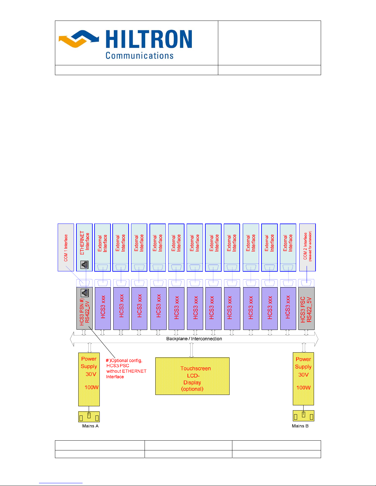
1 Overview
The controller HCS3 is a highly modular monitoring and control unit.
It comprises a 19”/2U modular mainframe with 13 interface connection slots designated A1 to
A13 located at the rear of the unit (refer to fig 1-1).
It can be equipped with two AC or DC power supplies for redundancy. The user interface
comprises a touch sensitive LCD display at the front panel and two communication card
modules type HCS3.PSC in slots A1 and A13 providing each a RS422 serial interface for
remote control. Alternatively, slot A1 can be equipped with a network interface card (NIC)
module type HCS3.PSN instead of HCS3.PSC providing both an Ethernet interface and a
serial interface. In addition, it is possible to renounce on the LCD display for cost reasons. In
this case, only remote control is available.
The remaining 11 interface connection slots (A2 to A12) can be equipped with different hotpluggable functional card modules like switch cards, I/O cards, signal I/O cards, etc whose
designation is HCS3.xxx where xxx defines the module type. This results in a very high flexibility. Thus, the controller is available in different versions by selection of the appropriate
functional card modules. The card modules are programmable to provide the functionality for
the various controller versions. Presently, the following versions are available:
1. Monitoring, control and power supply for fiber optic modules
2. Fiber optic N:1 switchover systems
3. LNB redundancy systems for C- and Ku-Band
4. HPA redundancy systems
5. Redundancy systems for DVB MPEG encoders/modulators/IRDs
6. Other applications for monitor&control
Each card module in the controller can be identified by its own ID-number used to access
and configure the module. Each HCS3 controller comes with an attached configuration sheet
showing the actual module configuration.

HILTRON GMBH
Stuttgarter Strasse 4
71522 Backnang
Tel.: + 49 (0) 7191 962660
Fax: + 49 (0) 7191 970022
Ust-IdNr. DE 12822829
Manual_HCS3_SSPA_A.doc Page 7 of 59
Date: 13.05.2008 Rev.: A
A1 A2 A3 A4 A5 A6 A7 A8 A9 A10 A12 A13A11
Power
Supply
A
Power
Supply
B
Fig 1-1: HCS3 controller, rear view
CONTROL UNIT HCS 3
HILTRON GMBH
Telecom Equipment
Fig 1-2: HCS3 controller, front view
HILTRON GMBH
Stuttgarter Strasse 4
71522 Backnang
Tel.: + 49 (0) 7191 962660
Fax: + 49 (0) 7191 970022
Ust-IdNr. DE 12822829
Manual_HCS3_SSPA_A.doc Page 8 of 59
Date: 13.05.2008 Rev.: A
2 Design
2.1 Mainframe
The mainframe of the HCS3 controller is a 19”/2U unit. Normally, front panel control is provided via a touch-sensitive LCD display type HCS3.TS. Alternatively, the controller can be
delivered without the LCD display.
As a standard, the controller is equipped with two hot-pluggable AC power supplies units with
IEC320 mains connectors located at the rear for power supply redundancy. As an option, DC
power supplies (24/48 VDC) are also available.
A sub chassis with a backplane interconnects all card modules via a serial bus. The following
bus lines are provided: data line, logic voltage +5V, supply voltage +26V and ground.
2.1.1 Schematic Diagram of the Controller
Fig 2.1.1-1: HCS3 Schematic Diagram

HILTRON GMBH
Stuttgarter Strasse 4
71522 Backnang
Tel.: + 49 (0) 7191 962660
Fax: + 49 (0) 7191 970022
Ust-IdNr. DE 12822829
Manual_HCS3_SSPA_A.doc Page 9 of 59
Date: 13.05.2008 Rev.: A
2.1.2 Technical Data
Size:
Width: 19“ rack-mountable
Height: 89 mm (3.5“, 2U)
Depth: 500 mm (20“, including connectors)
Temperature:
Operating: 0°C to +50°C
Non operating: -20°C to +80°C
Humidity:
Operating: 5% to 95% non condensing
Non operating: 0% to 100% non condensing
Power (per Input):
AC input: 95-245V; 47-63Hz; PFC
Consumption: max. 1A at 230V (dependent on configuration)
Max. Output Power (total): 90W
Serial Data Interfaces: (available on HCS3.PSC and HCS3.PSN)
RS422
Ethernet Interface: (only available if equipped with HCS3.PSN)
2.2 Display
The front panel LCD display (if fitted) is used for monitor and control of the controller and of
the devices connected thereto (e.g. fiber optic modules).
Rather than pressing buttons the operator has to touch the sensitive areas on the display.
The displayed icons and text based status messages vary with the specific configuration. By
means of a configuration program that comes with the controller the event handling, the sensitive areas and special text messages are widely configurable.
2.2.1 Technical Data
Size
Width: 128 Pixel LCD
Height: 64 Pixel LCD
Touch field 8 x 4 Pixel

HILTRON GMBH
Stuttgarter Strasse 4
71522 Backnang
Tel.: + 49 (0) 7191 962660
Fax: + 49 (0) 7191 970022
Ust-IdNr. DE 12822829
Manual_HCS3_SSPA_A.doc Page 10 of 59
Date: 13.05.2008 Rev.: A
3 Card assignment
The controller HCS3 is used to control redundant SSPA / HPA systems. Each module should
be plugged in to its dedicated location.
3.1 Card assignment of HCS3-SSPA/HPA
Each module should be plugged in to its dedicated location.
Card
Nr
Card Type Function Connect
A01 HCS3.PSN Supply and Communication. LAN
A02 HCS3.SWI HCS3 SWI-Card Module,
Control-Switch.
Switch01
A03 HCS3.SWI HCS3 SWI-Card Module,
Control-Switch.
Switch02
A04 HCS3.SWI HCS3 SWI-Card Module,
Control-Switch.
Switch03
A05 HCS3.SWI HCS3 SWI-Card Module,
Control-Switch.
Switch04
A06 HCS3.SWI HCS3 SWI-Card Module,
Control-Switch.
Switch05
A07 HCS3.SWI HCS3 SWI-Card Module,
Control-Switch.
Switch06
A08 HCS3.SWI HCS3 SWI-Card Module,
Control-Switch.
Switch07
A09 HCS3.SWI HCS3 SWI-Card Module,
Control-Switch.
Switch08
A10 HCS3.8CI Card Module for
Input of 8 Form C Contacts
A11 HCS3.OPK Card Module for
12 Outputs on Optical couplers
A12
A13 HCS3.PSC Supply and Communication.
The as-built configuration can be found in the attached separate HCS3 configuration
sheet

HILTRON GMBH
Stuttgarter Strasse 4
71522 Backnang
Tel.: + 49 (0) 7191 962660
Fax: + 49 (0) 7191 970022
Ust-IdNr. DE 12822829
Manual_HCS3_SSPA_A.doc Page 11 of 59
Date: 13.05.2008 Rev.: A
4 Modules
4.1 Communication (COM) Card Module (HCS3. PSN)
The COM card module type HCS3.PSN provides three functionalities.
1) Generates the internal DC voltage of 5V used as logic voltage.
2) Ethernet network interface card (NIC) to connect the controller to external network equipment like switches, hubs or computers.
3) Serial interface according to RS422 standard.
The Ethernet interface can be used in two ways:
• Web interface
• Remote control interface via UDP/IP protocol. It allows to integrate the controller in an
external network management system. The details of the remote control protocol are
published separately.
In most applications, the internal logic voltage and the 26V driver voltage shall be redundant.
Thus, two hot-pluggable COM card modules can be installed in each mainframe, type
HCS3.PSN or HCS3.PSC in slot A1 and type HCS3.PSC in slot A13. The 5V logic voltage as
well as the 26V driver voltage are constantly monitored
.
4.1.1 Location of Module
The modules are always located in:
¾ Slot A1: card module HCS3.PSN (with Ethernet and serial interface) or HCS3.PSC
(serial interface only)
4.1.2 Technical Data RS422
Communication Type RS422
Baud rate configurable
Data Bit configurable
Parity configurable
Stop bit configurable
The purpose of this serial interface is the connection of an extension module type RIO.8I
providing 8 digital inputs. Normally, it is not configured for serial remote control.

HILTRON GMBH
Stuttgarter Strasse 4
71522 Backnang
Tel.: + 49 (0) 7191 962660
Fax: + 49 (0) 7191 970022
Ust-IdNr. DE 12822829
Manual_HCS3_SSPA_A.doc Page 12 of 59
Date: 13.05.2008 Rev.: A
4.1.3 Pin-out for 9-pin Sub-D Connector male
Pin Function Comment
1 +5V Aux Voltage max. current 100mA
2 GND Connected with Pin 3+4
3 GND Connected with Pin 2+4
4 GND Connected with Pin 2+3
5 +5V Aux Voltage Connected with Pin 1
6 TX + RS 422
7 TX - RS 422
8 RX - RS 422
9 RX + RS 422
4.1.4 Input Interface Diagram / Electrical Diagram
VCC
RD
RO
DE
DI
GND
GND@2
A
B
Z
Y
14
2
3
4
5
7
6
12
11
10
9
IC2
MAX489
X1-9
X1-8
X1-7
X1-6

HILTRON GMBH
Stuttgarter Strasse 4
71522 Backnang
Tel.: + 49 (0) 7191 962660
Fax: + 49 (0) 7191 970022
Ust-IdNr. DE 12822829
Manual_HCS3_SSPA_A.doc Page 13 of 59
Date: 13.05.2008 Rev.: A
4.1.5 Technical Data Ethernet
Communication Type Ethernet
Bus interface IEEE802.3 (10BaseT)
Data transfer rate 10 Mbit/s
Connector RJ45
Max. length of cable 100m
4.1.6 Pin-out for Ethernet Connector RJ45
Pin Function Comment
1 TD+ Transmit +
2 TD- Transmit 3 RD+ Receive +
4 not used
5 not used
6 RD- Receive 7 not used
8 not used
4.1.7 Ethernet Interface Diagram

HILTRON GMBH
Stuttgarter Strasse 4
71522 Backnang
Tel.: + 49 (0) 7191 962660
Fax: + 49 (0) 7191 970022
Ust-IdNr. DE 12822829
Manual_HCS3_SSPA_A.doc Page 14 of 59
Date: 13.05.2008 Rev.: A
4.2 Communication (COM) Card Module (HCS3.PSC)
The COM card module type HCS3.PSC provides dual functionality.
1) Generates the internal DC voltage of 5V used as logic voltage.
2) Serial interface according to RS422 standard.
The serial interface can be used in two ways:
• Serial interface for configuration of the controller with a software called HCS3.Opto to
be installed on an external Windows PC connected to the controller via the serial interface. This is the method to configure the controller if the card module HCS3.PSN
with its Web interface is not available.
• Serial remote control interface if a module card HCS3.PSN with Ethernet interface is
not available. It allows to integrate the controller in an external network management
system. The details of the remote control protocol are published separately.
In most applications, the internal logic voltage and the 26V driver voltage shall be redundant.
Thus, two hot-pluggable COM card modules can be installed in each mainframe, type
HCS3.PSN or HCS3.PSC in slot A1 and type HCS3.PSC in slot A13. The 5V logic voltage as
well as the 26V driver voltage are constantly monitored
.
4.2.1 Location of Module
The modules are always located in:
¾ Slot A1: card module HCS3.PSN (with Ethernet and serial interface) or HCS3.PSC
(serial interface only)
¾ Slot A13: card module HCS3.PSC (serial interface only).
4.2.2 Technical Data
Communication Type RS422
Baud rate 9600 Baud
Data Bit 8 data
Parity no parity
Stop bit 1
Note:
The serial remote control interface is only available if the HCS3.PSN Ethernet commu-
nication card module is not fitted in slot A1.

HILTRON GMBH
Stuttgarter Strasse 4
71522 Backnang
Tel.: + 49 (0) 7191 962660
Fax: + 49 (0) 7191 970022
Ust-IdNr. DE 12822829
Manual_HCS3_SSPA_A.doc Page 15 of 59
Date: 13.05.2008 Rev.: A
4.2.3 Pin-out of 9-pin Sub-D Connector male
Pin Function Comment
1 +5V Aux Voltage max. current 100mA
2 GND Connected with Pin 3+4
3 GND Connected with Pin 2+4
4 GND Connected with Pin 2+3
5 +5V Aux Voltage Connected with Pin 1
6 TX + RS 422
7 TX - RS 422
8 RX - RS 422
9 RX + RS 422
4.2.4 Input Interface Diagram / Electrical Diagram
VCC
RD
RO
DE
DI
GND
GND@2
A
B
Z
Y
14
2
3
4
5
7
6
12
11
10
9
IC2
MAX489
X1-9
X1-8
X1-7
X1-6

HILTRON GMBH
Stuttgarter Strasse 4
71522 Backnang
Tel.: + 49 (0) 7191 962660
Fax: + 49 (0) 7191 970022
Ust-IdNr. DE 12822829
Manual_HCS3_SSPA_A.doc Page 16 of 59
Date: 13.05.2008 Rev.: A
4.3 HCS3 SWI-Card Module
The HCS3 SWI-Card Module is mainly be used as input/ output device for control and monitoring of Waveguide Switch SW
In total there are 4 actor outputs available which could be connected in parallel when higher
drive currents required.
4.3.1 Location of Module
The module is located in:
¾ See para. 3.1 Card assignment
4.3.2 Technical Data:
Actor Output: 26V 1A max
Measurement Input: 5%
4.3.3 Pin-out 9-pin Sub- D- Connector female for SWI Module
,0P
in
Function Comment Terminal Function
1 Input 1 Input Range 0..+50V D Sw-Pos A
2 Out 30V Supply for Sensors E Sw-Com
3 Ground GND B M-Com
4 Output 2 Actor Output 26V 1A max. C M-Pos B
5 Output 4 Actor Output 26V 1A max. A M-Pos A
6 Input 2 Input Range 0..+50V F Sw-Pos B
7 Ground GND B M-Com
8 Output 1 Actor Output 26V 1A max. C M-Pos B
9 Output 3 Actor Output 26V 1A max. A M-Pos A

HILTRON GMBH
Stuttgarter Strasse 4
71522 Backnang
Tel.: + 49 (0) 7191 962660
Fax: + 49 (0) 7191 970022
Ust-IdNr. DE 12822829
Manual_HCS3_SSPA_A.doc Page 17 of 59
Date: 13.05.2008 Rev.: A
4.3.4 Input Interface Diagram

HILTRON GMBH
Stuttgarter Strasse 4
71522 Backnang
Tel.: + 49 (0) 7191 962660
Fax: + 49 (0) 7191 970022
Ust-IdNr. DE 12822829
Manual_HCS3_SSPA_A.doc Page 18 of 59
Date: 13.05.2008 Rev.: A
4.4 HCS3.8CI-Card Module / Input to 8 Form C Contacts
The 8CI module provides a DC voltage of 26 V on the common pins via a protective resistor.
The input will be identified as active if the input voltage exceeds 12 V. The current is limited
to a maximum of 10 mA.
4.4.1 Location of Module
The module is located in:
¾ See para. 3.1 Card assignment
4.4.2 Technical Data
Input Voltage, max.: 26 V
Input active: > 10 V
4.4.3 Pin- Out 25-pin Sub- D- Connector female for 8CI Module
Pin Description Comment Function Address
1 NO Contact1
2 COMMON 1 Common X Redundancy
3 NC Contact1 Switch to X Redundancy CB.0
4 NO Contact2
5 COMMON 2 Common Y Redundancy
6 NC Contact2 Switch to Y Redundancy CB.1
7 NO Contact3
8 COMMON 3 Common Main
9 NC Contact3 Switch to Main CB.2
10 NO Contact4
11 COMMON 4 Common AUTOMATIC
12 NC Contact4 Switch to AUTOMATIC CB.3
13 NO Contact5
14 COMMON 5 Common MANUELL
15 NC Contact5 Switch to MANUELL CB.4
16 NO Contact6
17 COMMON 6
18 NC Contact6
19 NO Contact7
20 COMMON 7
21 NC Contact7
22 NO Contact8
23 COMMON 8
24 NC Contact8
25 Not Connected

HILTRON GMBH
Stuttgarter Strasse 4
71522 Backnang
Tel.: + 49 (0) 7191 962660
Fax: + 49 (0) 7191 970022
Ust-IdNr. DE 12822829
Manual_HCS3_SSPA_A.doc Page 19 of 59
Date: 13.05.2008 Rev.: A
4.4.4 Input Interface Diagram

HILTRON GMBH
Stuttgarter Strasse 4
71522 Backnang
Tel.: + 49 (0) 7191 962660
Fax: + 49 (0) 7191 970022
Ust-IdNr. DE 12822829
Manual_HCS3_SSPA_A.doc Page 20 of 59
Date: 13.05.2008 Rev.: A

HILTRON GMBH
Stuttgarter Strasse 4
71522 Backnang
Tel.: + 49 (0) 7191 962660
Fax: + 49 (0) 7191 970022
Ust-IdNr. DE 12822829
Manual_HCS3_SSPA_A.doc Page 21 of 59
Date: 13.05.2008 Rev.: A
4.5 HCS3.OPK Card Module for 12 Outputs on Optical couplers
The OPK module provides 12 outputs with optical coupler contacts corresponding to the internal bus signals.
4.5.1 Location of Module
The module is located in:
¾ See para. 3.1 Card assignment
4.5.2 Technical Data
Collector-Emitter Voltage: 80 VDC max
Emitter-Collector Voltage: 7 VDC max
Collector Current: 5 mA max
Collector Power Dissipation: 100 mW
The module needs one slot
4.5.3 Pin- Assignment of the 25-pin SubD- Connector (male)
Pin Description Comment Function
1 Gate1 Emitter Open Emitter
2 Gate2 Emitter Open Emitter
3 Gate3 Emitter Open Emitter
4 Gate4 Emitter Open Emitter
5 Gate5 Emitter Open Emitter
6 Gate6 Emitter Open Emitter
7 Gate7 Emitter Open Emitter
8 Gate8 Emitter Open Emitter
9 Gate9 Emitter Open Emitter
10 Gate10 Emitter Open Emitter
11 Gate11 Emitter Open Emitter
12 Gate12 Emitter Open Emitter
13 Not Connected
14 Gate1 Collector Open Collector
15 Gate2 Collector Open Collector
16 Gate3 Collector Open Collector
17 Gate4 Collector Open Collector
18 Gate5 Collector Open Collector
19 Gate6 Collector Open Collector
20 Gate7 Collector Open Collector
21 Gate8 Collector Open Collector
22 Gate9 Collector Open Collector
23 Gate10 Collector Open Collector
24 Gate11Collector Open Collector
25 Gate10 Collector Open Collector

HILTRON GMBH
Stuttgarter Strasse 4
71522 Backnang
Tel.: + 49 (0) 7191 962660
Fax: + 49 (0) 7191 970022
Ust-IdNr. DE 12822829
Manual_HCS3_SSPA_A.doc Page 22 of 59
Date: 13.05.2008 Rev.: A
4.5.4 Output Interface Diagram

HILTRON GMBH
Stuttgarter Strasse 4
71522 Backnang
Tel.: + 49 (0) 7191 962660
Fax: + 49 (0) 7191 970022
Ust-IdNr. DE 12822829
Manual_HCS3_SSPA_A.doc Page 23 of 59
Date: 13.05.2008 Rev.: A
5 Operation of the Controller via Front Panel
5.1 Main Screen of the Controller
After powering the controller starts with depicting the main screen on the LCD display. In
case there is no alarm to be monitored the controller is operated in he automatic mode
5.1.1 Main Screen in Automatic mode
The main screen show a simple block diagram of the redundant HPA / wave guide switch
section including the indication of
• switch position and alarms,
• the HPA alarms,
• the HCS-power supplies status,
• and the dehydrator alarms.
In the automatic mode the redundancy switches are configured in nominal position (see figure below). In case of an HPA alarm the relevant redundancy switch will be configured such
to replace the failed HPA by the redundant one. In this case the automatic operation mode
will be changed into the manual one.
Dehydrator WG-Switch (Antenna/Load)
Fig. 5-1: LCD Display – automatic operation mode
Power
supply
WG Switch
(red, config.)
HPA
The button
will open and display the Main Menu (see fig. 5-5 ). Selecting the button
“Manual” the automatic operation mode is changed into manual mode.

HILTRON GMBH
Stuttgarter Strasse 4
71522 Backnang
Tel.: + 49 (0) 7191 962660
Fax: + 49 (0) 7191 970022
Ust-IdNr. DE 12822829
Manual_HCS3_SSPA_A.doc Page 24 of 59
Date: 13.05.2008 Rev.: A
5.1.2 Main Screen in Manual mode
The main screen show the same simple block diagram of the redundant HPA / wave guide
switch section including the indication of
• switch position and alarms,
• the HPA alarms,
• the HCS-power supplies status,
• and the dehydrator alarms.
Additionally there are visible some control buttons for
• the selection of the transmit path
• the change of transmission signal to antenna (A) or dummy load (L)
• the change of the position of redundancy switch
1
23
4
D
H
Fig. 5-2: LCD Display – manual operation mode
The buttons
select the transmit path,. The selected path is indicated. The WGswitches belonging to this path can now be managed with buttons “L”, “A”, “R” and “M”
The function of the buttons “L”, “A”, “R” and “M” is explained in para. 5.2.
5.1.3 Explanation of Icons
Icon Description Comments
Power supply of controller:
Flashing when power supply is faulty, top
icon refers to power supply A (slot A01),
below icon refers to power supply B (slot
A13).
Icon in case of faulty power supply.
By touching the icon the sub screen
„Power Supply“ is selected.

HILTRON GMBH
Stuttgarter Strasse 4
71522 Backnang
Tel.: + 49 (0) 7191 962660
Fax: + 49 (0) 7191 970022
Ust-IdNr. DE 12822829
Manual_HCS3_SSPA_A.doc Page 25 of 59
Date: 13.05.2008 Rev.: A
Icon
Description Comments
Dehydrator
Icon for the dehydrator.
The icon is flashing in case of a dehydrator
alarm
HPA
Icon for the HPA.
The icon is flashing in case of a HPA alarm
Waveguide switch:
The line inside the symbols shows the signal
path direction.
Position A. (nominal position
Position B.
In case of failure or the switch is not connected there is no position indicated
The up- / down buttons select the transmit path,. The number of the selected
transmit path is displayed.
There are 4 transmit paths which
can be selected.
When the transmit path has been selected
this button will configure the relevant Antenna/Load switch to the load position (L =
Load).
The signal is
switched to the dummy load.
This button is only in manual operation mode visible.
When the transmit path has been selected
this button will configure the relevant Antenna/Load switch to the antenna position
(A = Antenna).
The signal is transmitted.
This button is only in manual operation mode visible.

HILTRON GMBH
Stuttgarter Strasse 4
71522 Backnang
Tel.: + 49 (0) 7191 962660
Fax: + 49 (0) 7191 970022
Ust-IdNr. DE 12822829
Manual_HCS3_SSPA_A.doc Page 26 of 59
Date: 13.05.2008 Rev.: A
Icon
Description
Comments
When the transmit path has been selected
this button will configure the relevant redundancy switch. The nominal HPA will be replaced by the redundant HPA.
(R = Replace / Redundant)
This button is only in manual operation mode visible.
This button will reconfigure the path which
was in redundant operation. The nominal
HPA will be in operation. The whole redundancy system is in nominal or main operation mode.
(M = Main)
This button is only in manual operation mode visible.
Backspace:
To selection screen
By touching the icon the screen „Selection Screen“ is selected.
5.2 Main Screen – Power Supply
Clicking on one of the two power supply icons on the main screen the
LCD display is showing the main parameters of the redundant power
supplies A and B
PwrSupp Unit A Unit B
InpVolt 26.0V 26.0V
LogVolt 5.35V 5.35V
LogCurr 120mA 110mA
Temp. 36°C 40°C
Fig. 5-3: Screen - Power Supply Fig. 5-4: Power Supply - Example for
nominal operation

HILTRON GMBH
Stuttgarter Strasse 4
71522 Backnang
Tel.: + 49 (0) 7191 962660
Fax: + 49 (0) 7191 970022
Ust-IdNr. DE 12822829
Manual_HCS3_SSPA_A.doc Page 27 of 59
Date: 13.05.2008 Rev.: A
5.2.1 Explanation of Screen
Icon Description Comment
PwrSupp Designation of sub screen Display of power supply values.
Unit A Values of this column refer to power
supply A (HCS3.PSN or
HCS3.PSC).
Unit B Values of this column refer to power
supply B (HCS3.PSC).
InpVolt Input voltages of power supply unit Voltage shall be between 25.0 and 27.0 V.
LogVolt Voltage of logic voltage supply in
front of the diode.
Voltage across the diode is approx.
0.4 V at 200 mA current.
Voltage shall be between 4.8V and 5.5V.
LogCurr Current of logic voltage supply. Depending on the power supply toler-
ances, current will be supplied by only one
unit or by both units by load sharing.
Temp. Temperature of power supply card. The temperature is approx. 20 degrees
above the ambient temperature. The card
temperature shall not exceed 85°C.
Back to main screen.
5.2.2 Status Messages of a Power Supply Module
Display Comment Range
Main Module A(B)
26 V
Supply voltage of Main Power supply A (B). 26 V +/- 1V
Logic Voltage 5.2V. Supply voltage of Com Power supply 1 (2). 5.3 V +/- 0.25V
Logic Current 200 mA Current consumption of the controller. < 250 mA
Card Temp +35°C Internal Controller Temperature. < 65° C

HILTRON GMBH
Stuttgarter Strasse 4
71522 Backnang
Tel.: + 49 (0) 7191 962660
Fax: + 49 (0) 7191 970022
Ust-IdNr. DE 12822829
Manual_HCS3_SSPA_A.doc Page 28 of 59
Date: 13.05.2008 Rev.: A
5.3 Main Menu
Fig. 5-5: Main Menu
5.3.1 Explanation of Screen
Icon Description Comment
Forward Manual:
By touching the forward icon to change in to the
Manual mode. The screen „ Main Screen in Manual
mode “ is selected.
Forward Automatic:
By touching the forward icon to change in to the
Automatic mode. The screen „ Main Screen in Automatic mode “ is selected.
Forward Display:
By touching the forward icon the sub screen „Display“
is selected.
Backspace:
By touching the backspace icon leads back to the
Main screen.
5.4 Screen - Display

HILTRON GMBH
Stuttgarter Strasse 4
71522 Backnang
Tel.: + 49 (0) 7191 962660
Fax: + 49 (0) 7191 970022
Ust-IdNr. DE 12822829
Manual_HCS3_SSPA_A.doc Page 29 of 59
Date: 13.05.2008 Rev.: A
5.4.1 Explanation of Screen
Icon Description Comment
Contrast
The contrast can be adjusted in the
sub screen “Display” by using the
+/- buttons.*
Variation in range of 18 to 49 possible.
Backlight
The backlight can be adjusted in the
sub screen “Display” by using the
+/- buttons.
Variation in range of 00 to 63 possible.
Increases the numerical value.
reduces the numerical value.
Leads back to the sub screen.
HCS3
Serial-Nr.
e.g. 0257718.
HCS3
Programversion.
Info on implemented software e.g.
Program V.2.1.
* Remark:
Setting the numeric value for contrast from 49 (see comments) to 50. (limits). The new value
will ( instead of 50) start with 18 again. This will lead to a very weak picture. Stepping this
process several times will yield to satisfying results. On technical reasons this function could
not prevented.

HILTRON GMBH
Stuttgarter Strasse 4
71522 Backnang
Tel.: + 49 (0) 7191 962660
Fax: + 49 (0) 7191 970022
Ust-IdNr. DE 12822829
Manual_HCS3_SSPA_A.doc Page 30 of 59
Date: 13.05.2008 Rev.: A
6 Web-Interface for HCS3
If the controller HCS3 is equipped with a COM card module type HCS3.PSN in slot A1, it can
be completely monitored and controlled via its Web interface. The following section describes
this interface in detail.
In order to use the Web interface, the following prerequisites must be met:
• A PC directly connected to the controller or via an IP network (please refer to section 7)
• A standard web browser (e.g. Internet Explorer version 6 or higher) installed on this PC
• Java Runtime Engine (JRE version 1.5 or higher) installed (can be downloaded from
www.sun.com
)
• Appropriate IP settings of the COM card module (please refer to section 7)
The Web interface is started by typing the correct IP address into the Web browser.
6.1 View on the Web Interface
When the Web interface is started the block diagram with HPA redundancy configuration and
the antenna / load switching is displayed on the screen. The screen content consists of 3
functional areas:
• the HPA redundancy (HPA icons & redundancy switches)
• the antenna / load switching
• the common, general area with following functions
o monitoring & control for peripheral signals
o setting of mainly SNMP parameters (system configuration)
o monitoring & control for communication modules with the monitoring of power
supply parameters.
The figure below shows the top view of the web interface.

HILTRON GMBH
Stuttgarter Strasse 4
71522 Backnang
Tel.: + 49 (0) 7191 962660
Fax: + 49 (0) 7191 970022
Ust-IdNr. DE 12822829
Manual_HCS3_SSPA_A.doc Page 31 of 59
Date: 13.05.2008 Rev.: A
6.1.1 General Information
To manage the controller via Web-interface there are three different user access settings:
• a “default” access mode
• a “no password” access mode
• a “User level” access mode
More detailed information you will find in paragraph 6.4 System Control.
The controller is configured when it is delivered in “default” access mode
HPA redundancy control Antenna / Load switching
Peripheral
signals
System config.
SNMP, Web
Communication Card Modules
(communication, red. power supply)

HILTRON GMBH
Stuttgarter Strasse 4
71522 Backnang
Tel.: + 49 (0) 7191 962660
Fax: + 49 (0) 7191 970022
Ust-IdNr. DE 12822829
Manual_HCS3_SSPA_A.doc Page 32 of 59
Date: 13.05.2008 Rev.: A
When you want to change a parameter first click on the button "Control". Then you will be
asked for a password, which is the same for all parameters and which you only have to enter
once per open web interface. This protects the system against unauthorized parameter
changes.
.
Enter the default setting for access
User: HCS
Password: hiltron
6.1.2 Explanation of Icons
Icon Explanation
Switch position is unknown
(e.g. switch is not connected and no position is indicated)
The switch is configured to position A
for redundancy Switch ≡ position MAIN
for antenna./load switch ≡ position ANTENNA
The switch is configured to position B
for redundancy Switch ≡ position RED
for antenna./load switch ≡ position LOAD
The switching function is faulty.
In case of a failure of the switch (e.g. command and no response
on indicated position. )
The icon presents the HPA (e.g. HPA2). There is no failure indicated (green) and the HPA is active in the redundancy circuitry.
The HPA (e.g. HPA 3) is excluded from the redundancy switching.
The icon is indicated grey colored.
In the case the relevant HPA is activated (e.g. HPA 1) and is faulty
the icon is indicated red colored. (Faults on inactivated HPA will not
be displayed red colored.)

HILTRON GMBH
Stuttgarter Strasse 4
71522 Backnang
Tel.: + 49 (0) 7191 962660
Fax: + 49 (0) 7191 970022
Ust-IdNr. DE 12822829
Manual_HCS3_SSPA_A.doc Page 33 of 59
Date: 13.05.2008 Rev.: A
6.2 Redundancy Control
6.2.1 Redundant HPA
This icon represents the redundant HPA
(SSPA). By clicking on this icon, a new window opens with status information enabling
the user to set and read available parameters
and informs the user about the existing alarms
if any.
The first text line informs about the status.
The second line shows the “link name” which
can bet set by the user (see below). This
name should be a unique name of the card
and be chosen according to the application.
The Status Tab
The status tab comprises available status information on the operation mode of the redundant HPA.
Following status information depending on the
operation mode and configuration is available:
• Automatic
• Main
• PATH 1 RED
• PATH 2 RED
• PATH 3 RED
• PATH 4 RED
It is not possible to change any parameters in
this tab.

HILTRON GMBH
Stuttgarter Strasse 4
71522 Backnang
Tel.: + 49 (0) 7191 962660
Fax: + 49 (0) 7191 970022
Ust-IdNr. DE 12822829
Manual_HCS3_SSPA_A.doc Page 34 of 59
Date: 13.05.2008 Rev.: A
The Parameter Tab
Clicking on the tab Parameter a list of parameter groups is presented:
• Configuration
• Set Mode
• Aux for Redundancy
¾ Parameter (group): Configuration
When Configuration is selected the parameter Name (e.g SSPA Redundancy) is displayed. The name can be changed by overwriting and confirming with OK.
This “name” is shown in the second line of the
icon
This name should be a unique name of the
card and be chosen according to the application
¾ Parameter (group): Set Mode
When Set Mode is selected the parameter
“Position” with a list field is presented. The
list field allows the selection of the redundancy operation mode.
It allows to select the automatic mode or to
select one of the 4 available paths (e.g. Path
1 RED) to be replaced by the redundant
HPA.
The mode “Main” reconfigures the setting of
switches into nominal configuration where
there is no automatic redundancy switching
operation.
The automatic mode switches to automatic
redundancy mode.

HILTRON GMBH
Stuttgarter Strasse 4
71522 Backnang
Tel.: + 49 (0) 7191 962660
Fax: + 49 (0) 7191 970022
Ust-IdNr. DE 12822829
Manual_HCS3_SSPA_A.doc Page 35 of 59
Date: 13.05.2008 Rev.: A
¾ Parameter group: Aux for Redundancy
This parameter allow to include (or edit)
additional cards into alarm management
of the redundant HPA. If any auxiliary
alarm is available and in the card setting
released the redundant HPA will not take
over the operation for a failed HPA. The
automatic mode is blocked.
With the list field the number of additional
cards (with auxiliary alarms) can be selected
Any selected number of additional cards will create an additional line in the parameter group
“Aux for Redundancy”.
For example, with 1 card you will get:
Clicking on “Redundancy Aux” following
parameters are visible:
Card Address:
The slot number of the selected card
(e.g. A10) is displayed.
Signal 1..8:
There are 8 alarm inputs available
(Card type HCS2.8CI) with the possibility to choose “used” or “unused”.

HILTRON GMBH
Stuttgarter Strasse 4
71522 Backnang
Tel.: + 49 (0) 7191 962660
Fax: + 49 (0) 7191 970022
Ust-IdNr. DE 12822829
Manual_HCS3_SSPA_A.doc Page 36 of 59
Date: 13.05.2008 Rev.: A
6.2.2 Nominal HPA
This icons represent the transmit path consisting
of the HPA and the pair of switches. By clicking
on one of these icons, a new window opens with
status information enabling the user to set and
read available parameters and informs the user
on the existing alarms if any.
The first text line informs about the location of
the card in the HCS3 controller and the function
name of the card.
The second line shows the “name” (e.g. equipment) which can bet set by the user (see below).
This name should be a unique name for the interfacing card.
The Status Tab
The status tab comprises available status information on the operation mode of the redundant HPA.
Position:
Display of following possible status information (Position of switch)
• Main
• Red
Mute Request:
Indicates if the controller wants to mute the
HPA in order to switch-over to the redundant HPA or vice versa.
It is not possible to change any parameters in
this tab.

HILTRON GMBH
Stuttgarter Strasse 4
71522 Backnang
Tel.: + 49 (0) 7191 962660
Fax: + 49 (0) 7191 970022
Ust-IdNr. DE 12822829
Manual_HCS3_SSPA_A.doc Page 37 of 59
Date: 13.05.2008 Rev.: A
The Parameter Tab
Clicking on the tab Parameter a list of parameter groups is presented:
• Configuration
• Cardinfo
• Position Names
• Config SwitchOver
¾ Parameter (group): Configuration
When Configuration is selected the parameter Name (e.g HPA 1) is displayed. The
name can be changed by overwriting and
confirming with OK.
This “name” is shown in the second line of
the icon.
This name should be a unique name of the
interfacing card.
¾ Parameter (group): Cardinfo
When Cardinfo is selected the table with
information on used card type (HCS3.SWI
for switch control) is displayed.
The information are:
• Module type
• Program Version (used software)
• Card ID (unique ID)
¾ Parameter (group): Position Names
When Position Names is selected the
names for “Default Pos” and “Switched Pos”
are displayed. The name could be changed
if necessary.
This names are presented in the status tab.

HILTRON GMBH
Stuttgarter Strasse 4
71522 Backnang
Tel.: + 49 (0) 7191 962660
Fax: + 49 (0) 7191 970022
Ust-IdNr. DE 12822829
Manual_HCS3_SSPA_A.doc Page 38 of 59
Date: 13.05.2008 Rev.: A
¾ Parameter (group): Config SwitchOver
Auxiliary Cards:
This parameter allow to include (or remove)
additional cards into alarm management of the
redundant HPA. In case of an auxiliary alarm
is continuously present in the adjusted period
– see parameter Delay Time - the switchover
process for the relevant HPA will be triggered.
With the list field the number of additional
cards (with auxiliary alarms) can be selected
Selecting the parameter group Config
SwitchOver of HPA all parameters for
setting for the redundancy control are
visible.
Delay Time [sec]:
Setting of the delay period between
the occurrence of an alarm and the
triggering of the message „Switchover request“ to initiate a switchover
to a redundant link
Switchover:
With the help of the list field (enable,
disable) the relevant HPA in the
transmission path can be included
or excluded from the redundancy
switching processing.
Any selected number of additional cards will create an additional line in the parameter group
“Position Aux”.
For example, with 1 card you will get following:
Clicking on “Redundancy Aux” following parameters are visible:
Card Address:
The slot number of the selected
card (e.g. A10) is displayed.
Signal 1..8:
There are 8 alarm inputs available (Card type HCS2.8CI) with
the choice “used” or “unused”.

HILTRON GMBH
Stuttgarter Strasse 4
71522 Backnang
Tel.: + 49 (0) 7191 962660
Fax: + 49 (0) 7191 970022
Ust-IdNr. DE 12822829
Manual_HCS3_SSPA_A.doc Page 39 of 59
Date: 13.05.2008 Rev.: A
The Alarm Tab
Selecting the alarms tab the alarms - if any - related to function of the card are displayed.
The format of an alarm message is as follows:
alarm number, colon, name of the alarm. The
alarm name enables the operator to determine
whether it is only a wrong parameter setting or the
card itself is corrupt.

HILTRON GMBH
Stuttgarter Strasse 4
71522 Backnang
Tel.: + 49 (0) 7191 962660
Fax: + 49 (0) 7191 970022
Ust-IdNr. DE 12822829
Manual_HCS3_SSPA_A.doc Page 40 of 59
Date: 13.05.2008 Rev.: A
6.3 Antenna / Load Control
The switch icons (marked area)
present the antenna/load switching. By
clicking on one of these icons a new
window opens with the status information enabling the user to set and read
available parameters and informs the
user on the existing alarms if any.
The Status Tab
The status tab comprises available status
information on the operation mode of the
redundant HPA.
Position:
Display of the present position of the antenna/load switch (either “Antenna” or
“Load”)
Mute Request:
Indicates if the controller wants to mute
the HPA in order to switch-over to the
redundant HPA or vice versa.
It is not possible to change any parameters
in this tab.

HILTRON GMBH
Stuttgarter Strasse 4
71522 Backnang
Tel.: + 49 (0) 7191 962660
Fax: + 49 (0) 7191 970022
Ust-IdNr. DE 12822829
Manual_HCS3_SSPA_A.doc Page 41 of 59
Date: 13.05.2008 Rev.: A
The Parameter Tab
Clicking on the tab Parameter a list of parameter groups is presented:
• Configuration
• Cardinfo
• Position Names
• Set Switch
¾ Parameter (group): Configuration
When Configuration of ANT 1…. is selected
the parameter Name is displayed. The name
(e.g. ANT1) presents the designation of the
relevant switch and can be changed by typing
in the entry field a new name.
This name should be a unique name for the
card.
¾ Parameter (group): Cardinfo
When Cardinfo is selected the table with
information of used card/module type
(HCS3.SWI for switch control) is displayed.
The information are:
• Module type
• Program Version (used software)
• Card ID (unique ID)
¾ Parameter (group): Position Names
When Position Names is selected the
names for the default and switched position
are displayed. For the application the names
“Antenna” and “Dummy” have been chosen
and can be edited if necessary.
These names are presented in status tab
and are displayed if you want to change the
switch position.
Æ parameter group: set switch

HILTRON GMBH
Stuttgarter Strasse 4
71522 Backnang
Tel.: + 49 (0) 7191 962660
Fax: + 49 (0) 7191 970022
Ust-IdNr. DE 12822829
Manual_HCS3_SSPA_A.doc Page 42 of 59
Date: 13.05.2008 Rev.: A
¾ Parameter (group): Set Switch
Selecting the parameter group Set
Switch the antenna / load switch can
be configured.
The list field present the position names
“Antenna” and “Dummy” of the selected
switch.
.
The Alarm Tab
Selecting the alarms tab the alarms - if any related to function of the card are displayed.
The format of an alarm message is as follows:
alarm number, colon, name of the alarm. The
alarm name enables the operator to determine
whether it is only a wrong parameter setting or
the card itself is corrupt.

HILTRON GMBH
Stuttgarter Strasse 4
71522 Backnang
Tel.: + 49 (0) 7191 962660
Fax: + 49 (0) 7191 970022
Ust-IdNr. DE 12822829
Manual_HCS3_SSPA_A.doc Page 43 of 59
Date: 13.05.2008 Rev.: A
6.4 Auxiliary Input
The icon (see
marked area) allows to manage auxiliary inputs for additional alarms
(e.g. alarms of a dehydrator etc.)
By clicking on this icon, a new window opens with a Parameter and an
Alarm tab is opening.
The Parameter Tab
In the parameter tab you can set and
change the parameter values of the
card/module. For this click on the
respective nodes at the upper part of
the window. All parameters are displayed, but some of them are read
only.
The parameter groups containing all
essential parameters are listed in the
parameter tab
HILTRON GMBH
Stuttgarter Strasse 4
71522 Backnang
Tel.: + 49 (0) 7191 962660
Fax: + 49 (0) 7191 970022
Ust-IdNr. DE 12822829
Manual_HCS3_SSPA_A.doc Page 44 of 59
Date: 13.05.2008 Rev.: A
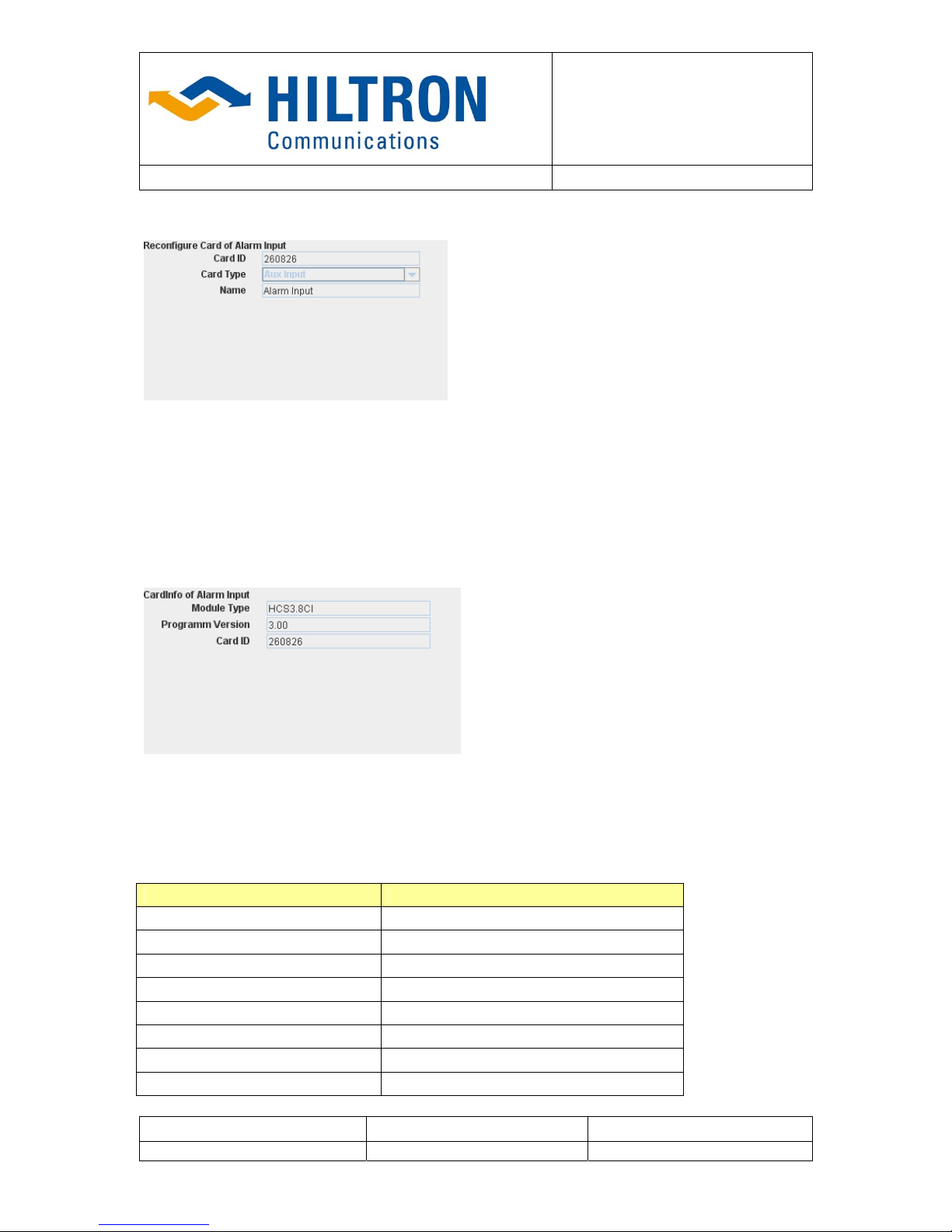
¾ Parameter (group): Reconfigure Card
By clicking on the parameter group “Reconfigure Card …” the parameters belonging to this
group are presented on the window.
CardID:
This value is unique and cannot be
changed.
management select “non”
CardType:
The required card type “Aux Input” has be set. If no input module is available or you want
it to exclude it from the alarm.
Name:
The name (e.g. Alarm Input) presents the designation of the function or a card’s name
and can be changed if necessary
¾ Parameter (group): CardInfo
All parameter values are read only values
and cannot be changed
By clicking on the parameter group “CardInfo”
the parameters belonging to this group are
presented on the window.
Module Type
Type of the card module
Program Version
Version of the card specific software
Card ID
Unique card module identification no.
With the next following Signal parameter groups Signal
n (….) n= 1…8 the available 8 input
groups of the Input Module HCS3.8CI on the 25-pin SubD- Connector can be configured:
Signal parameter group configures input signals on
Signal1 (1-2-3) pin#1 and pin #3 w.r.t. pin #2
Signal2 (4-5-6) pin#4 and pin #6 w.r.t. pin #5
Signal3 (7-8-9) pin#7 and pin #9 w.r.t. pin #8
Signal4 (10-11-12) pin#10 and pin #12 w.r.t. pin #11
Signal5 (13-14-15) pin#13 and pin #15 w.r.t. pin #14
Signal6 (16-17-18) pin#16 and pin #18 w.r.t. pin #18
Signal7 (19-20-21) pin#19 and pin #21 w.r.t. pin #20
Signal8 (22-23-24) pin#22 and pin #24 w.r.t. pin #23

HILTRON GMBH
Stuttgarter Strasse 4
71522 Backnang
Tel.: + 49 (0) 7191 962660
Fax: + 49 (0) 7191 970022
Ust-IdNr. DE 12822829
Manual_HCS3_SSPA_A.doc Page 45 of 59
Date: 13.05.2008 Rev.: A
¾ Parameter (group): Signal1 (1-2-3)
By clicking on the parameter group “Signal1 (1-2-3)” the parameters belonging to
the group become visible in the lower
part or the window.
Pin 1 (NO) Voltage
Present the (logic signal) level on Pin 1
The logic function of Pin 1 is “NO” with reference to Pin 2 .
Pin 3 (NC) Voltage
Present the (logic signal) level on Pin 3
The logic function of Pin 3 is “NC” with reference to Pin 2 .
Name
The entry and information field allows to enter or to edit the alarm signal name.
Config
The different logic functions of the input group (pin1, pin2 and pin3) can be selected and
configured.
clicking to “Config” a list field is opening and allow different settings
Possibility of Setting Function
Not assigned The alarm input is inactive
Signal on open Pin 1 (NO) An alarm will be generated when Pin1 is open
(no connection to Pin 2)
Alarm on closed Pin 1 (NO)
An alarm will be generated when Pin1 is closed
(connection to Pin 2)
Alarm on open Pin 3 (NO) An alarm will be generated when Pin3 is open
(no connection to Pin 2)
Alarm on closed Pin 3 (NO) An alarm will be generated when Pin3 is closed
(connection to Pin 2)
Form C Contact An alarm will be generated when Pin1 is open and Pin3
is closed (connection to Pin 2)
Inverse Form C Contact An alarm will be generated when Pin3 is open and Pin1
is closed (connection to Pin 2)

HILTRON GMBH
Stuttgarter Strasse 4
71522 Backnang
Tel.: + 49 (0) 7191 962660
Fax: + 49 (0) 7191 970022
Ust-IdNr. DE 12822829
Manual_HCS3_SSPA_A.doc Page 46 of 59
Date: 13.05.2008 Rev.: A
In the same way the parameters belonging to the parameter groups “input signal #2” up to
“input signal #8” can be configured.
The Alarm Tab
Selecting the alarms tab the alarms - if any related to function of the card are displayed.
The format of an alarm message is as follows:
alarm number, colon, name of the alarm. The
alarm name enables the operator to determine
whether it is only a wrong parameter setting or
the card itself is corrupt.

HILTRON GMBH
Stuttgarter Strasse 4
71522 Backnang
Tel.: + 49 (0) 7191 962660
Fax: + 49 (0) 7191 970022
Ust-IdNr. DE 12822829
Manual_HCS3_SSPA_A.doc Page 47 of 59
Date: 13.05.2008 Rev.: A
6.5 Communication Card Module (HCS3.PSN & HCS3.PSC)
The icons
(see marked area) allows to monitor
and control the communication card
modules HCS3.PSN as well HCS3.PSC
which are redundant power supplies
and care for network communication.
By clicking on one of these icons, the
status is displayed.
The Status Tab
The status tab comprises the basic card parameters like voltage and current. These values
can also be read from the local display of the
HCS3 if available.
It is not possible to change any parameter in
this tab.

HILTRON GMBH
Stuttgarter Strasse 4
71522 Backnang
Tel.: + 49 (0) 7191 962660
Fax: + 49 (0) 7191 970022
Ust-IdNr. DE 12822829
Manual_HCS3_SSPA_A.doc Page 48 of 59
Date: 13.05.2008 Rev.: A
The Parameter Tab
In the parameter tab you can set and change the
parameter values of the card/module. For this
click on the respective nodes at the upper part of
the window. All parameters are displayed, but
some of them are read only..
When you want to change a parameter first click on the button "Control". Then you will be
asked for a password, which is the same for all parameters and which you only have to enter
once per open web interface. This protects the system against unauthorized parameter
changes. After authorization, click again on the button "Control", type in the new value and
click the "OK" button to activate the changes. Whenever you change the configuration of a
card, a restart of the Web interface is required.
¾Parameter (group): Reconfigure Card
By clicking on the parameter group “Reconfigure Card …” the parameters belonging to this
group are presented on the window.
CardName:
The name (e.g. SSPA PSN) presents the
designation of the function or a card’s
name and can be changed if necessary
¾Parameter (group): CardInfo
All parameter values are read only values
and cannot be changed
By clicking on the parameter group “CardInfo of
…” the parameters belonging to this group are
presented on the window.
Module Type
Type of the card module
Program Version
Version of the card specific software
Card ID
Unique card module identification no.

HILTRON GMBH
Stuttgarter Strasse 4
71522 Backnang
Tel.: + 49 (0) 7191 962660
Fax: + 49 (0) 7191 970022
Ust-IdNr. DE 12822829
Manual_HCS3_SSPA_A.doc Page 49 of 59
Date: 13.05.2008 Rev.: A
The Alarm Tab
Selecting the alarms tab the alarms - if any - related to function of the card are displayed.
The format of an alarm message is as follows:
alarm number, colon, name of the alarm. The
alarm name enables the operator to determine
whether it is only a wrong parameter setting or the
card itself is corrupt.

HILTRON GMBH
Stuttgarter Strasse 4
71522 Backnang
Tel.: + 49 (0) 7191 962660
Fax: + 49 (0) 7191 970022
Ust-IdNr. DE 12822829
Manual_HCS3_SSPA_A.doc Page 50 of 59
Date: 13.05.2008 Rev.: A
6.6 System Control
The icon
(see marked
area) allows to manage the system environment (e.g. the Web-interface and
the SNMP parameters).
By clicking on this icon, a new window
opens with a Parameter and an Alarm
tab.
The Parameter Tab
In the parameter tab you can set and change
the parameter values of the card. For this
click on the respective nodes at the upper
part of the window. All parameters are displayed, but some of them are read only.
This window will be displayed when the option SNMP is not activated.
The parameter groups containing all essential parameters are listed in the parameter
tab
When SNMP is activated additional parame-
ter groups
• SNMP Configurations
• Trap Configurations
• Community Names
are released.

HILTRON GMBH
Stuttgarter Strasse 4
71522 Backnang
Tel.: + 49 (0) 7191 962660
Fax: + 49 (0) 7191 970022
Ust-IdNr. DE 12822829
Manual_HCS3_SSPA_A.doc Page 51 of 59
Date: 13.05.2008 Rev.: A
¾ Parameter (group): Set Device Name
Please note for SNMP application!
This parameter “Name” is used for SNMP as
the device name. When traps in case of a failure are sent this name will be included in the
trap message.
By clicking on the parameter group “Set
Device Name” the parameter “Name” can
be entered or edited. This name is shown
in the second line of the icon.
Default setting for name is “System Name”.
¾ Parameter (group): Register SNMP
To activate the SNMP option select the parameter group Register SNMP. This parameter group is only present on the window
when SNMP is not activated.
Card ID
Unique card module identification no.
SNMP Key
This key is required to activate the
SNMP operation mode.
This key is related to specific card ID.
How to activate?
In case of the customer orders the option for SNMP operation after the delivery of a HCS3
controller, the card ID is required to generate the SNMP key. Setting the correct key and confirming with “OK” the SNMP option is enabled and permanently active.
¾ Parameter (group): SNMP Configurations
In the parameter group “SNMP Configuration”
additional information like system description,
location and contact address are managed.
This parameter are sent in the trap message in
case of a malfunction or change of setting.
Therefore they are important.
This information can be also be retrieved from
the SNMPv2-MIB

HILTRON GMBH
Stuttgarter Strasse 4
71522 Backnang
Tel.: + 49 (0) 7191 962660
Fax: + 49 (0) 7191 970022
Ust-IdNr. DE 12822829
Manual_HCS3_SSPA_A.doc Page 52 of 59
Date: 13.05.2008 Rev.: A
Explanation of parameters
Parameter Description
System Description Input for system information
Location Input for information on location of the equipment.
Contact Input for contact information (address). e.g. in case of malfunctions
¾ Parameter (group): Trap Configuration
In the parameter group “Trap Configuration”
up to 4 trap destinations can be put
Traps
The sending of traps can be enabled or disabled. The SNMP-version can be set.
Authentication Traps
When enabled an additional warning trap
message is generated in when a wrong
community name is set.
When disabled no authentication trap will
be sent.
¾ Parameter (group): Community Names
By clicking on the parameter group “Community Names” the parameters belonging to
this group are presented on the window.
Explanation of parameters
Parameter Description
Write Community Definition of the community for setting of parameters.
Read Community
Definition of the community for getting of parameters.
Trap Community The Trap Community will only sent by the traps.
The Community names should fit exactly to the names used in the system. Please mind capital and small letters.

HILTRON GMBH
Stuttgarter Strasse 4
71522 Backnang
Tel.: + 49 (0) 7191 962660
Fax: + 49 (0) 7191 970022
Ust-IdNr. DE 12822829
Manual_HCS3_SSPA_A.doc Page 53 of 59
Date: 13.05.2008 Rev.: A
¾ Parameter (group): Security
The parameter group “Security” allows to set
different user access rights for managing the
controller.
With the parameters mode the operator can
choose between tree different access options.
No Password:
When “no password” is selected there is
no registration necessary if the want to
change any setting of parameters. Everybody is allowed to change parameters
without restrictions. (The sub branches
below the main branch “Security” will not
be visible anymore.)
Default:
When “Default” is selected and set the
operator has to enter the default setting
User: HCS
Password: hiltron
when he wants to change any parameter.
User Level:
When “User Level” is selected the administrator can assign the user rights in
three categories.
The category “user” allows the user only
operational activities, e.g. to configure a
switch.
The category “Supervisor” allows the
user to edit current and voltage limits.
The category “administrator” allows the
operator high level work, e.g. to configure
cards
Overview on different security levels
According to the hierarchical structure of the user rights the user 4 posses more rights than
user 3, e.g. the user 4 can change the passwords of user 3, 2 and 1 but not
vice versa.
The next figure show the hierarchical structure.

HILTRON GMBH
Stuttgarter Strasse 4
71522 Backnang
Tel.: + 49 (0) 7191 962660
Fax: + 49 (0) 7191 970022
Ust-IdNr. DE 12822829
Manual_HCS3_SSPA_A.doc Page 54 of 59
Date: 13.05.2008 Rev.: A
How to set a User Level?
Select the parameter group “Security” and
choose “User Level”.
Choose below the parameter group Secu-
rity the group with the required access level.
e.g. Administrator.
Put in the user(name) and the password.
The access right now configured. The user
is logged in on the administrator level.
Choose below the parameter group Secu-
rity the group with the required access level.
e.g. Supervisor.
Put in the user(name) and the password.
The access right now configured. The user
is logged in on the supervisor level.

HILTRON GMBH
Stuttgarter Strasse 4
71522 Backnang
Tel.: + 49 (0) 7191 962660
Fax: + 49 (0) 7191 970022
Ust-IdNr. DE 12822829
Manual_HCS3_SSPA_A.doc Page 55 of 59
Date: 13.05.2008 Rev.: A
Choose below the parameter group Secu-
rity the group with the required access level.
e.g. User.
Put in the user(name) and the password.
The access right now configured. The user
is logged in on the user level.
How to log in?
Choose below the parameter group Security the group with the required access level.
e.g. User.
Put in the user(name) and the password.
The user is logged in on the user level.
Contingency Solution
In case the passwords are lost/forgotten or generally there is no access to manage the controller, a master password could be generated with the help of the ID of the card (PSN).

HILTRON GMBH
Stuttgarter Strasse 4
71522 Backnang
Tel.: + 49 (0) 7191 962660
Fax: + 49 (0) 7191 970022
Ust-IdNr. DE 12822829
Manual_HCS3_SSPA_A.doc Page 56 of 59
Date: 13.05.2008 Rev.: A
Security Level - Access to Parameters
Access Level
Para Modules / Cards Parameter Group Parameter User Super-
visor
Administrator
6.2 Redundancy
Control
6.2.1 Redundant HPA Configuration Name X X
Set Mode Position X X X
Aux for Redun-
dancy
Additional cards X
Redundancy Aux X X
6.2.2 Nominal HPA Configuration Name X X
Cardinfo Info-Para.
Position Names Default Pos
Switched Pos
X
X
Config SwitchOver Time Delay
Auxiliary Cards
Switchover
X
X
6.3 Antenna Load Configuration Name X X
Cardinfo Info-Para.
Position Names Default Pos
Switched Pos
X
X
Set Switch Position X X X
6.4 Aux Input Reconfigure Card Card ID
Card type
Name
X
X
X
X
CardInfo Info-Para.
Signal1 (1-2-3) Pin (NO) voltage
Pin (NC) voltage
Config
Name
X
X
6.5 Communication
Card Module
Reconfigure Card Card Name X X
CardInfo Info-Para.
6.6 System Control Set Device Name Device Name X
Register SNMP Card ID
SNMP Key
X
SNMP Configura-
tions
System descript.
Location
Contact
X
X
X
Trap Configuration Traps
Auth.Traps
Trap desitnation
X
X
X
X

HILTRON GMBH
Stuttgarter Strasse 4
71522 Backnang
Tel.: + 49 (0) 7191 962660
Fax: + 49 (0) 7191 970022
Ust-IdNr. DE 12822829
Manual_HCS3_SSPA_A.doc Page 57 of 59
Date: 13.05.2008 Rev.: A
Access Level
Para Modules / Cards Parameter Group Parameter User Super-
visor
Administrator
Community Names Write Community
Read Community
Trap Community
X
X
X
Security Mode X
The Alarm Tab
In the alarms tab the alarms - if any - related to function of the card are displayed. For the
system configuration module for the time being no alarm are defined. No alarm will be indicated.

HILTRON GMBH
Stuttgarter Strasse 4
71522 Backnang
Tel.: + 49 (0) 7191 962660
Fax: + 49 (0) 7191 970022
Ust-IdNr. DE 12822829
Manual_HCS3_SSPA_A.doc Page 58 of 59
Date: 13.05.2008 Rev.: A
7 Setting the IP-Address
Prior to operation of the network interface card (NIC) type HCS3.PSN , the operator shall set
the NIC’s IP address. There is a special configuration program on the CD provided with the
controller. In order to configure the card, the following equipment is required:
• The HCS3 Controller with the NIC type HCS3.PSN fitted in slot A1.
• A PC running Microsoft Windows operating system equipped with CD-ROM drive and
Ethernet network interface card.
• A CAT5/6 crossover network cable or a Ethernet hub/switch and two standard net-
work cables to connect the HCS3.PSN to the PC.
• The CD-ROM shipping with the HCS3 Controller.
On the CD-ROM you will find in the directory the folder SCConfig.
Select the file setup.exe and start the installation. The installation assistant will guide you
through the installation steps.
By default a new folder SCConfig will
be generated. Click on the button to
confirm the proposed directory.
After the successful installation a shortcut SCConfig
has been generated and installed in the windows
main menu “Programs”.
Follow the recommendation and restart the Windows program.
Setting the NIC’s IP parameters is easily done within a few minutes.
1. Install the network cable between the NIC and your PC. Simply connect them directly
with a crossover cable. Alternatively, connect both, the PC and the NIC to the same
network hub/switch by using two straight network cables. It is essential that the computer and the NIC are connected to the same network segment. Otherwise, the configuration program is not able to find the NIC.

HILTRON GMBH
Stuttgarter Strasse 4
71522 Backnang
Tel.: + 49 (0) 7191 962660
Fax: + 49 (0) 7191 970022
Ust-IdNr. DE 12822829
Manual_HCS3_SSPA_A.doc Page 59 of 59
Date: 13.05.2008 Rev.: A
2. Select in the Windows menu Programs
the folder SCConfig.
Double-click on the 'SCConfig' program.
The configuration program for the NIC is
started and opens with following window:.
3. Click on the button “Search” and the program is searching for the NIC.
4. The program shows in the combo box at
least one entry describing the actual
network configuration of the NIC. The
network parameters of the NIC are presented in the dialog boxes below.
5. Fill in the dialog the fields IP Address, Network mask and, if necessary, Gateway with
appropriate values. Make sure, that the 'DHCP' box is unchecked
6. In case of a DHCP configuration is required enable DHCP.
7. Press the SET button to apply the new settings to your NIC.
Now the IP configuration of the HCS3.PSN is completed. You may finally want to test if the
card is accessible now. Start your web browser and type the NIC’s IP address into the URL
field of the browser. The NIC should reply with its main page, provided the NIC and your PC
are configured for the same subnet.
 Loading...