

hilscher NXHX 90-JTAG Device Description
Device description
NXHX 90-JTAG
Development board
Hilscher Gesellschaft für Systemautomation mbH
www.hilscher.com
DOC170202HW03EN | Revision 3 | English | 2019-01 | Released | Public

Table of contents 2/82
Table of contents
1 Introduction .............................................................................................................................. 4
1.1 About this document ........................................................................................................4
1.1.1 Description of the contents ............................................................................... 4
1.1.2 List of revisions ................................................................................................. 4
1.1.3 Conventions in this document...........................................................................4
1.1.4 Reference to hardware ..................................................................................... 4
1.2 Other relevant documentation..........................................................................................5
1.3 Legal notes.......................................................................................................................6
2 Descriptions and drawings ................................................................................................... 10
2.1 Key features ...................................................................................................................10
2.2 Overview ........................................................................................................................11
2.2.1 Block diagram ................................................................................................. 11
2.2.2 Positions of interfaces and operating elements .............................................. 12
2.3 Operating elements........................................................................................................14
2.3.1 S400 – Slide switches for console mode and alternative boot mode.............. 14
2.3.2 S401 – Reset push button .............................................................................. 16
2.3.3 S700 – Slide switches for user-defined inputs ................................................ 16
2.3.4 S701 – Slide switches for selecting JTAG, UART, ADCs and user LEDs ...... 16
2.4 Interfaces .......................................................................................................................17
2.4.1 X400 – JTAG connector.................................................................................. 17
2.4.2 X500 – Ethernet connectors ........................................................................... 18
2.4.3 X600 – Host interface ..................................................................................... 19
2.4.4 X601 – SPM host interface connector via SQI/SPI.........................................26
2.4.5 X700 – ADC pin header .................................................................................. 27
2.4.6 X900 – Connector for NXHX fieldbus adapter modules.................................. 28
2.4.7 X901 – Connector for NXHX-ENC, NXHX-IOL and standard MMIOs ............ 29
2.4.8 X902 – Connector for NXHX-RS232 adapter module (UART) ....................... 30
2.4.9 X1000 – Mini-B USB connector ...................................................................... 31
2.4.10 X1001 – Measuring points (vias) for UART via FTDI......................................31
2.4.11 X1200 – Connector for +24V power supply ................................................... 32
2.5 LEDs ..............................................................................................................................33
3 Accessories............................................................................................................................35
3.1 Devices for host interface...............................................................................................35
3.1.1 Overview ......................................................................................................... 35
3.1.2 NXHX-SDRSPM: SDRAM and Serial Dual-Port Memory (via USB) at host
interface .......................................................................................................... 35
3.1.3 NXHX-FTDI: Serial Dual-Port Memory via USB device at host interface ....... 38
3.1.4 NXPCA-PCI: Parallel Dual-Port Memory at host interface.............................. 40
3.1.5 Accessory cables and connectors for host interface....................................... 41
3.2 Fieldbus interface adapter modules ...............................................................................42
3.2.1 Overview ......................................................................................................... 42
3.2.2 NXHX-DP........................................................................................................ 43
3.2.3 NXHX-CO ....................................................................................................... 43
3.2.4 NXHX-DN........................................................................................................ 44
3.2.5 NXHX-CC........................................................................................................ 44
3.3 NXHX-RS232 serial interface adapter ...........................................................................45
3.4 NXHX-ENC module........................................................................................................46
3.5 NXHX-IOL module .........................................................................................................48
NXHX 90-JTAG | Device description
DOC170202HW03EN | Revision 3 | English | 2019-01 | Released | Public
© Hilscher 2019

Table of contents 3/82
3.6 NXAC-POWER voltage supply unit................................................................................51
4 Reference................................................................................................................................ 52
4.1 Schematic diagrams.......................................................................................................52
4.1.1 Schematics NXHX 90-JTAG ........................................................................... 52
4.1.2 Schematics of the accessory devices ............................................................. 63
4.2 Bills of materials .............................................................................................................72
4.2.1 NXHX 90-JTAG............................................................................................... 72
4.2.2 NXHX-SDRSPM ............................................................................................. 75
4.2.3 NXHX-FTDI..................................................................................................... 76
4.2.4 NXHX-ENC ..................................................................................................... 77
4.3 Matrix label.....................................................................................................................78
4.4 Technical data NXHX 90-JTAG .....................................................................................78
List of figures ......................................................................................................................... 79
List of tables........................................................................................................................... 80
Contacts.................................................................................................................................. 82
NXHX 90-JTAG | Device description
DOC170202HW03EN | Revision 3 | English | 2019-01 | Released | Public
© Hilscher 2019
Introduction 4/82
1 Introduction
1.1 About this document
1.1.1 Description of the contents
This document describes the hardware of the NXHX 90-JTAG development
board.
1.1.2 List of revisions
Index Date Revision
1 2017-06-22 Document created
2 2018-11-15 Document revised according to hardware revision 3
3 2019-01-08 Caption of table 30 on page 37 changed from “Pinning host
interface of NXHX-SDRSPI device” (typo) to “Pinning host
interface of NXHX-SDRSPM device”
Table1: List of revisions
1.1.3 Conventions in this document
# means active low signal
Notes are marked as follows:
Important:
<Important note>
Note:
<Simple note>
<Note, where to find further information>
1.1.4 Reference to hardware
Hardware Revision Part number
NXHX 90-JTAG 3 7833.000
Table2: Reference to hardware
NXHX 90-JTAG | Device description
DOC170202HW03EN | Revision 3 | English | 2019-01 | Released | Public
© Hilscher 2019

Introduction 5/82
1.2 Other relevant documentation
Besides this device description, the following documents are also relevant
to the user of the NXHX 90-JTAG development board:
Title Contents Document ID
Getting started: netX Studio CDT – netX 90
development
netX 90 – Technical data reference guide Describes netX 90 chip functions DOC160609TRGxxEN
netX 90 – Design-In Guide Describes the standard circuitry around the
Table3: Additional documentation
Getting started guide for netX 90 SoC
development with netX Studio CDT (for
software developers)
netX interfaces (for hardware developers)
DOC170504GSxxEN
DOC180501DGxxEN
NXHX 90-JTAG | Device description
DOC170202HW03EN | Revision 3 | English | 2019-01 | Released | Public
© Hilscher 2019

Introduction 6/82
1.3 Legal notes
Copyright
© Hilscher Gesellschaft für Systemautomation mbH
All rights reserved.
The images, photographs and texts in the accompanying materials (in the
form of a user's manual, operator's manual, Statement of Work document
and all other document types, support texts, documentation, etc.) are
protected by German and international copyright and by international trade
and protective provisions. Without the prior written consent, you do not
have permission to duplicate them either in full or in part using technical or
mechanical methods (print, photocopy or any other method), to edit them
using electronic systems or to transfer them. You are not permitted to make
changes to copyright notices, markings, trademarks or ownership
declarations. Illustrations are provided without taking the patent situation
into account. Any company names and product designations provided in
this document may be brands or trademarks by the corresponding owner
and may be protected under trademark, brand or patent law. Any form of
further use shall require the express consent from the relevant owner of the
rights.
Important notes
Utmost care was/is given in the preparation of the documentation at hand
consisting of a user's manual, operating manual and any other document
type and accompanying texts. However, errors cannot be ruled out.
Therefore, we cannot assume any guarantee or legal responsibility for
erroneous information or liability of any kind. You are hereby made aware
that descriptions found in the user's manual, the accompanying texts and
the documentation neither represent a guarantee nor any indication on
proper use as stipulated in the agreement or a promised attribute. It cannot
be ruled out that the user's manual, the accompanying texts and the
documentation do not completely match the described attributes, standards
or any other data for the delivered product. A warranty or guarantee with
respect to the correctness or accuracy of the information is not assumed.
We reserve the right to modify our products and the specifications for such
as well as the corresponding documentation in the form of a user's manual,
operating manual and/or any other document types and accompanying
texts at any time and without notice without being required to notify of said
modification. Changes shall be taken into account in future manuals and do
not represent an obligation of any kind, in particular there shall be no right
to have delivered documents revised. The manual delivered with the
product shall apply.
Under no circumstances shall Hilscher Gesellschaft für Systemautomation
mbH be liable for direct, indirect, ancillary or subsequent damage, or for
any loss of income, which may arise after use of the information contained
herein.
NXHX 90-JTAG | Device description
DOC170202HW03EN | Revision 3 | English | 2019-01 | Released | Public
© Hilscher 2019

Introduction 7/82
Liability disclaimer
The hardware and/or software was created and tested by Hilscher
Gesellschaft für Systemautomation mbH with utmost care and is made
available as is. No warranty can be assumed for the performance or
flawlessness of the hardware and/or software under all application
conditions and scenarios and the work results achieved by the user when
using the hardware and/or software. Liability for any damage that may have
occurred as a result of using the hardware and/or software or the
corresponding documents shall be limited to an event involving willful intent
or a grossly negligent violation of a fundamental contractual obligation.
However, the right to assert damages due to a violation of a fundamental
contractual obligation shall be limited to contract-typical foreseeable
damage.
It is hereby expressly agreed upon in particular that any use or utilization of
the hardware and/or software in connection with
· Flight control systems in aviation and aerospace;
· Nuclear fusion processes in nuclear power plants;
· Medical devices used for life support and
· Vehicle control systems used in passenger transport
shall be excluded. Use of the hardware and/or software in any of the
following areas is strictly prohibited:
· For military purposes or in weaponry;
· For designing, engineering, maintaining or operating nuclear systems;
· In flight safety systems, aviation and flight telecommunications systems;
· In life-support systems;
· In systems in which any malfunction in the hardware and/or software
may result in physical injuries or fatalities.
You are hereby made aware that the hardware and/or software was not
created for use in hazardous environments, which require fail-safe control
mechanisms. Use of the hardware and/or software in this kind of
environment shall be at your own risk; any liability for damage or loss due
to impermissible use shall be excluded.
NXHX 90-JTAG | Device description
DOC170202HW03EN | Revision 3 | English | 2019-01 | Released | Public
© Hilscher 2019

Introduction 8/82
Warranty
Hilscher Gesellschaft für Systemautomation mbH hereby guarantees that
the software shall run without errors in accordance with the requirements
listed in the specifications and that there were no defects on the date of
acceptance. The warranty period shall be 12 months commencing as of the
date of acceptance or purchase (with express declaration or implied, by
customer's conclusive behavior, e.g. putting into operation permanently).
The warranty obligation for equipment (hardware) we produce is 36
months, calculated as of the date of delivery ex works. The aforementioned
provisions shall not apply if longer warranty periods are mandatory by law
pursuant to Section 438 (1.2) BGB, Section 479 (1) BGB and Section 634a
(1) BGB [Bürgerliches Gesetzbuch; German Civil Code] If, despite of all
due care taken, the delivered product should have a defect, which already
existed at the time of the transfer of risk, it shall be at our discretion to
either repair the product or to deliver a replacement product, subject to
timely notification of defect.
The warranty obligation shall not apply if the notification of defect is not
asserted promptly, if the purchaser or third party has tampered with the
products, if the defect is the result of natural wear, was caused by
unfavorable operating conditions or is due to violations against our
operating regulations or against rules of good electrical engineering
practice, or if our request to return the defective object is not promptly
complied with.
Costs of support, maintenance, customization and product care
Please be advised that any subsequent improvement shall only be free of
charge if a defect is found. Any form of technical support, maintenance and
customization is not a warranty service, but instead shall be charged extra.
Additional guarantees
Although the hardware and software was developed and tested in-depth
with greatest care, Hilscher Gesellschaft für Systemautomation mbH shall
not assume any guarantee for the suitability thereof for any purpose that
was not confirmed in writing. No guarantee can be granted whereby the
hardware and software satisfies your requirements, or the use of the
hardware and/or software is uninterruptable or the hardware and/or
software is fault-free.
It cannot be guaranteed that patents and/or ownership privileges have not
been infringed upon or violated or that the products are free from third-party
influence. No additional guarantees or promises shall be made as to
whether the product is market current, free from deficiency in title, or can be
integrated or is usable for specific purposes, unless such guarantees or
promises are required under existing law and cannot be restricted.
NXHX 90-JTAG | Device description
DOC170202HW03EN | Revision 3 | English | 2019-01 | Released | Public
© Hilscher 2019

Introduction 9/82
Confidentiality
The customer hereby expressly acknowledges that this document contains
trade secrets, information protected by copyright and other patent and
ownership privileges as well as any related rights of Hilscher Gesellschaft
für Systemautomation mbH. The customer agrees to treat as confidential all
of the information made available to customer by Hilscher Gesellschaft für
Systemautomation mbH and rights, which were disclosed by Hilscher
Gesellschaft für Systemautomation mbH and that were made accessible as
well as the terms and conditions of this agreement itself.
The parties hereby agree to one another that the information that each
party receives from the other party respectively is and shall remain the
intellectual property of said other party, unless provided for otherwise in a
contractual agreement.
The customer must not allow any third party to become knowledgeable of
this expertise and shall only provide knowledge thereof to authorized users
as appropriate and necessary. Companies associated with the customer
shall not be deemed third parties. The customer must obligate authorized
users to confidentiality. The customer should only use the confidential
information in connection with the performances specified in this
agreement.
The customer must not use this confidential information to his own
advantage or for his own purposes or rather to the advantage or for the
purpose of a third party, nor must it be used for commercial purposes and
this confidential information must only be used to the extent provided for in
this agreement or otherwise to the extent as expressly authorized by the
disclosing party in written form. The customer has the right, subject to the
obligation to confidentiality, to disclose the terms and conditions of this
agreement directly to his legal and financial consultants as would be
required for the customer's normal business operation.
Export provisions
The delivered product (including technical data) is subject to the legal
export and/or import laws as well as any associated regulations of various
countries, especially such laws applicable in Germany and in the United
States. The products / hardware / software must not be exported into such
countries for which export is prohibited under US American export control
laws and its supplementary provisions. You hereby agree to strictly follow
the regulations and to yourself be responsible for observing them. You are
hereby made aware that you may be required to obtain governmental
approval to export, reexport or import the product.
Terms and conditions
Please read the notes about additional legal aspects on our netIOT web
site under http://www.netiot.com/netiot/netiot-edge/terms-and-
conditions/.
NXHX 90-JTAG | Device description
DOC170202HW03EN | Revision 3 | English | 2019-01 | Released | Public
© Hilscher 2019

Descriptions and drawings 10/82
2 Descriptions and drawings
2.1 Key features
The NXHX 90-JTAG is a development board for the netX 90 SoC featuring:
· Host interface connector by use case:
– Companion chip with host interface: 8/16 bit parallel dual-port
memory, 2 x SPI/SQI as serial dual-port memory
– Stand-alone chip application: 16 bit SDRAM, MII for Ethernet PHY,
and custom-specific module solutions
· Additional host interface pin header connector for serial dual-port
memory (SPM0) via SPI/SQI
· JTAG MIPI-20 interface for debugging
· On-board JTAG-to-USB adapter (FTDI) for OpenOCD
· On-board UART-to-USB adapter (FTDI) for diagnosis/firmware
download
· USB Mini-B connector for JTAG-to-USB debugging and UART-to-USB
diagnosis/firmware download via FTDI
· 2-port RJ45 Ethernet interface with “Link” and “Activity” LEDs
· Interface for NXHX “legacy fieldbus” modules
(PROFIBUS, CANopen, DeviceNet and CC-Link)
· 4MB SQI Flash
· RS-232 serial interface
· Encoder interface with BiSS, SSI or EnDat connectivity
· Analog-to-digital converter (ADC) interface
· MMIO connectivity
· System status LED, power LED and two communication status LEDs
· Switches for configuring alternative boot option and console modes
· Four user output LEDs and four input dip switches
· Reset push button
· Power connector jack for +24 V
NXHX 90-JTAG | Device description
DOC170202HW03EN | Revision 3 | English | 2019-01 | Released | Public
© Hilscher 2019
Descriptions and drawings 11/82
2.2 Overview
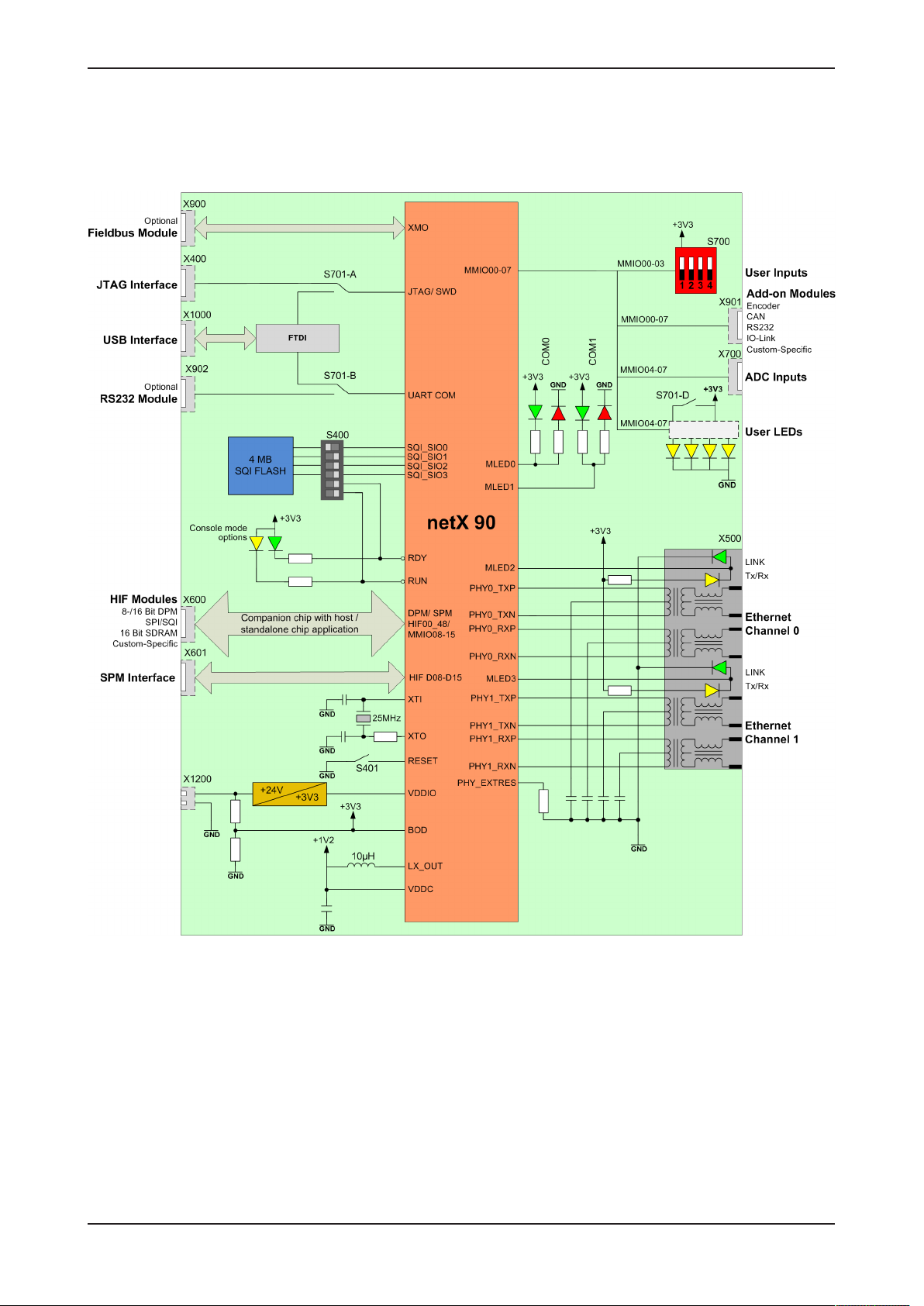
2.2.1 Block diagram
Figure1: NXHX 90-JTAG block diagram
NXHX 90-JTAG | Device description
DOC170202HW03EN | Revision 3 | English | 2019-01 | Released | Public
© Hilscher 2019
Descriptions and drawings 12/82
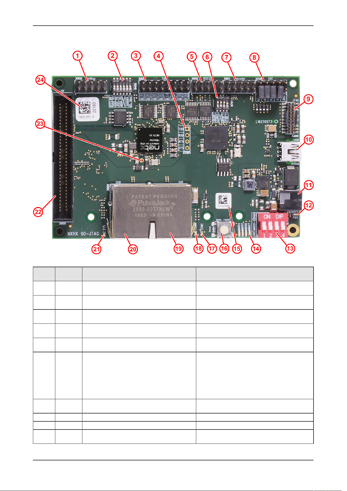
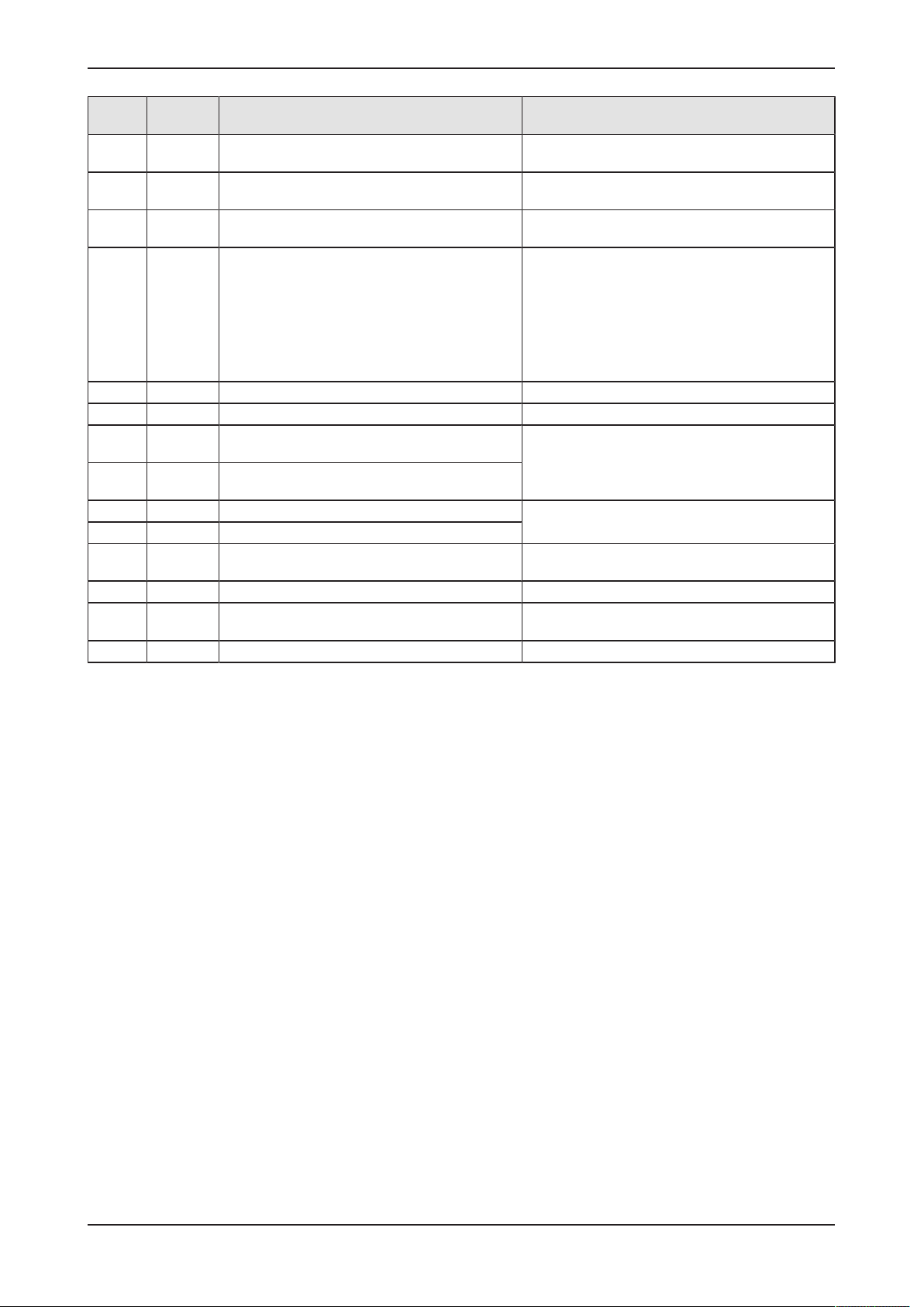
2.2.2 Positions of interfaces and operating elements
Figure2: Positions on NXHX 90-JTAG
No. in
figure
Name Description For details see section
(1) X900 Connector for NXHX fieldbus adapter modules X900 – Connector for NXHX fieldbus adapter
modules [}page28]
(2) S400 Slide switches for selecting console mode and
alternative boot mode
(3) X601 Serial Dual Port Memory (SPM) host interface
connector for SQI/SPI
(4) X1001 Measuring points (vias) for UART via FTDI X1001 – Measuring points (vias) for UART via
(5) X902 Connector for NXHX-RS232 adapter module X902 – Connector for NXHX-RS232 adapter
(6) S701 Slide switches for:
· Configuring JTAG interface
(via 20 pin connector or USB jack)
· Configuring UART interface
(via NXHX-RS232 connector or USB jack)
· Enabling user LEDs or ADCs
(7) X901 Connector for NXHX-ENC module, NXHX-IOL
(IO Link) module, MMIO and BiSS signals
(8) X700 ADC pin header
(9) X400 JTAG MIPI-20 connector
(10) X1000 Mini-B USB connector for debugging and
diagnosis via FTDI
S400 – Slide switches for console mode and
alternative boot mode [}page14]
X601 – SPM host interface connector via SQI/
SPI [}page26]
FTDI [}page31]
module (UART) [}page30]
S701 – Slide switches for selecting JTAG, UART,
ADCs and user LEDs [}page16]
X901 – Connector for NXHX-ENC, NXHX-IOL
and standard MMIOs [}page29]
X700 – ADC pin header [}page27]
X400 – JTAG connector [}page17]
X1000 – Mini-B USB connector [}page31]
NXHX 90-JTAG | Device description
DOC170202HW03EN | Revision 3 | English | 2019-01 | Released | Public
© Hilscher 2019
Descriptions and drawings 13/82
No. in
figure
Name Description For details see section
(11) X1200 24 V DC power supply connector (jack for
barrel connector)
(12) PWR
(P1202)
(13) S700 Slide switches for user-defined input S700 – Slide switches for user-defined
(14) MMIO4
(P700)
MMIO5
(P701)
MMIO6
(P702)
MMIO7
(P703)
(15) P101 AOI label –
(16) S401 Reset push button
(17) COM1
(P501)
(18) COM0
(P500)
(19) X500 (B) RJ45 connector Ethernet channel 1 (CH1)
(20) X500 (A) RJ45 connector Ethernet channel 0 (CH0)
(21) SYS
(P400)
(22) X600 Host interface connector
(23) X300 Reference voltage connector (via) for ADCs
(24) P102 Matrix label
Power LED
User definable LEDs (output)
COM1 LED (communication status)
COM0 LED (communication status)
SYS LED (system status)
(VREF_ADC)
Table4: Positions on printed circuit board
X1200 – Connector for +24V power
supply [}page32]
LEDs [}page33]
inputs [}page16]
LEDs [}page33]
S401 – Reset push button [}page16]
LEDs [}page33]
X500 – Ethernet connectors [}page18]
LEDs [}page33]
X600 – Host interface [}page19]
X700 – ADC pin header [}page27]
Matrix label [}page78]
NXHX 90-JTAG | Device description
DOC170202HW03EN | Revision 3 | English | 2019-01 | Released | Public
© Hilscher 2019

Descriptions and drawings 14/82
2.3 Operating elements
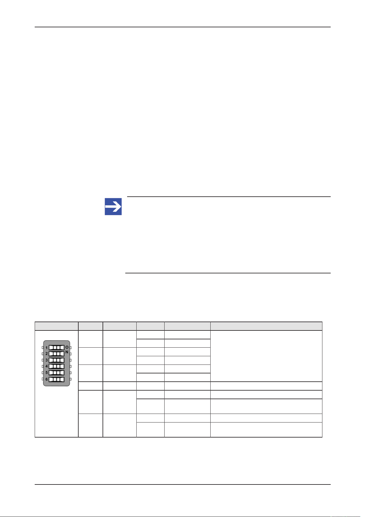
2.3.1 S400 – Slide switches for console mode and alternative boot mode
For identifying the switches on the board, see position (2) in section
Positions of interfaces and operating elements [}page12].
Standard boot mode
In standard boot mode, the ROM code searches for a valid firmware and
– if available – starts it. If the ROM code cannot find a valid “regular”
firmware, it tries to start a valid “maintenance” firmware instead. If neither
“regular” nor “maintenance” firmware is found, the ROM code automatically
enters console mode.
S400 settings for standard boot mode:
Switch 5 = OFF
Switch 6 = OFF
Console mode
The ROM code of the netX 90 features a console mode that enables the
handling of firmware programming depending on the selected console
mode interface, e.g. via UART, via Ethernet, etc. Thus you can download a
firmware file to the flash memory of the device, e.g. from your development
PC by using the “flasher tool” of netX Studio CDT.
Note:
The verification of the ROM code using the final silicon chip is not
yet completed. Therefore, initially, we recommend using the default
console mode by keeping switches 1, 2 and 3 of S400 in OFF
position. A full description of the console modes will be provided
after the verification.
Note also that downloading a firmware to the netX 90 is possible via
the JTAG interface. You can use the on-board JTAG-to-USB
connection, as described in the Getting started: netX Studio CDT –
netX 90 development, DOC170504GSxxEN, (in chapter How to ...
Use the Flasher tool).
S400 settings for console mode:
Switch 5 = ON
Switch 6 = OFF or ON
NXHX 90-JTAG | Device description
DOC170202HW03EN | Revision 3 | English | 2019-01 | Released | Public
© Hilscher 2019
Descriptions and drawings 15/82
Alternative boot mode
In alternative boot mode, the ROM code starts the “maintenance”
firmware instead of the “regular” firmware. The maintenance firmware is
capable of programming a new firmware (firmware update).
Potential use cases are:
· Firmware update procedures:
A new firmware received via web server or host interface is stored
either on-chip in INTFLASH1 or off-chip in an externally connected SQI
Flash. A software reset cycle initiated by a software command or a
hardware reset cycle (by S401 reset button or power-on) while switch 6
is at ON position starts a maintenance firmware, which programs the
new firmware.
· Multiple firmware versions:
The netX 90 has a maintenance firmware stored in INTFLASH1 and
holds multiple firmware versions for different Real-Time Ethernet
protocols in an externally connected SQI Flash. The maintenance
firmware programs the firmware selected by the system integrator, e.g.
via a rotary DIP-switch (or other ways).
Note:
The alternative boot mode is not yet supported because the
required “maintenance firmware“ is still under development.
Note also that if console mode and alternative boot mode are both
enabled (i.e. if switch 5 and 6 are both in ON position), the console
mode always has priority over the alternative boot mode.
If e.g. a power loss disrupts the programming of the new firmware,
the ROM code detects that the procedure is incomplete and restarts the maintenance firmware without prior selection.
S400 settings for alternative boot mode:
Switch 5 = OFF
Switch 6 = ON
Description of the S400 switches
S400 Switch Signal Position Connects to Function
1 SQI_SIO2 OFF Internal pull-up Reserved for future use (keep switches in
ON GND via 4.7 kΩ
2 SQI_SIO1 OFF Internal pull-up
ON GND via 4.7 kΩ
3 SQI_SIO0 OFF Internal pull-up
ON GND via 4.7 kΩ
4 Not used - - -
5 RDY OFF Internal pull-up Disables console mode
ON GND via 1 kΩ Enables console mode
6 RUN OFF Internal pull-up Disables alternative boot mode
ON GND via 1 kΩ Enables alternative boot mode
Table5: S400 for configuring console mode and alternative boot mode
OFF position).
Note: In the final version of the netX 90
ROM code, these switches will configure the
console mode.
(currently only UART)
(not yet supported)
NXHX 90-JTAG | Device description
DOC170202HW03EN | Revision 3 | English | 2019-01 | Released | Public
© Hilscher 2019
Descriptions and drawings 16/82
2.3.2 S401 – Reset push button
For identifying the button on the board, see position (16) in section
Positions of interfaces and operating elements [}page12] .
S401 Signal Connects to Function
RST_IN# GND Resets the netX
Table6: S401 – Reset button
2.3.3 S700 – Slide switches for user-defined inputs
For identifying the switches on the board, see position (13) in section
Positions of interfaces and operating elements [}page12].
S700 Switch Signal Position Connects to
1 MMIO00/ENDAT0_IN/BISS0_SL OFF Internal pull-down
ON +3.3V via 1 kΩ
2 MMIO01/ENDAT0_OUT/BISS0_MO OFF Internal pull-down
ON +3.3V via 1 kΩ
3 MMIO02/ENDAT0_OE/BISS0_OE OFF Internal pull-down
ON +3.3V via 1 kΩ
4 MMIO03/ENDAT0_CLK/BISS0_MA OFF Internal pull-down
ON +3.3V via 1 kΩ
Table7: S700 for user-defined inputs
2.3.4 S701 – Slide switches for selecting JTAG, UART, ADCs and user LEDs
For identifying the switches on the board, see position (6) in section
Positions of interfaces and operating elements [}page12]
S701 Switch Name Position Function
1 JTAG OFF Enable JTAG via FTDI (JTAG-to-USB: use Mini
USB connector for debugging)
ON Enable JTAG via JTAG connector (use JTAG
MIPI-20 connector for debugging)
2 UART OFF Enable UART via FTDI (UART-to-USB: use
Mini USB connector for diagnosis/firmware
download)
ON Enable UART via RS232 (use NXHX-RS232 at
X902 for diagnosis/firmware download)
3 Not connected
4 User
LEDs
Table8: S701 miscellaneous configuration
OFF Enable ADCs (disables user LEDs)
ON Enable user LEDs (disables ADCs)
NXHX 90-JTAG | Device description
DOC170202HW03EN | Revision 3 | English | 2019-01 | Released | Public
© Hilscher 2019

Descriptions and drawings 17/82
2.4 Interfaces
2.4.1 X400 – JTAG connector
JTAG MIPI-20 connector X400. For identifying the connector on the board,
see position (9) in section Positions of interfaces and operating
elements [}page12].
Note:
To enable this interface, put switch 1 of S701 into ON position (see
position (6) in section Positions of interfaces and operating
elements [}page12]).
JTAG Pin Signal
MIPI-20-ARM
ARM-20-JTAG
1 +3V3 3V3
2 TMS SWDIO
3 GND GND
4 TCLK SWDCLK
5 GND GND
6 TDO TRACE_CTL
7 Not connected Not connected
8 TDI Not connected
9 GND GND
10 RESET# RESET#
11 GND GND
12 Not connected TRACE_CLK
13 GND GND
14 MLED0 TRACE_DATA_0
15 GND GND
16 MLED1 TRACE_DATA_1
17 GND GND
18 MLED2 TRACE_DATA_2
19 GND GND
20 MLED3 TRACE_DATA_3
Table9: Pin assignments MIPI-20 JTAG connector
ARM-20-SWD
NXHX 90-JTAG | Device description
DOC170202HW03EN | Revision 3 | English | 2019-01 | Released | Public
© Hilscher 2019
Descriptions and drawings 18/82
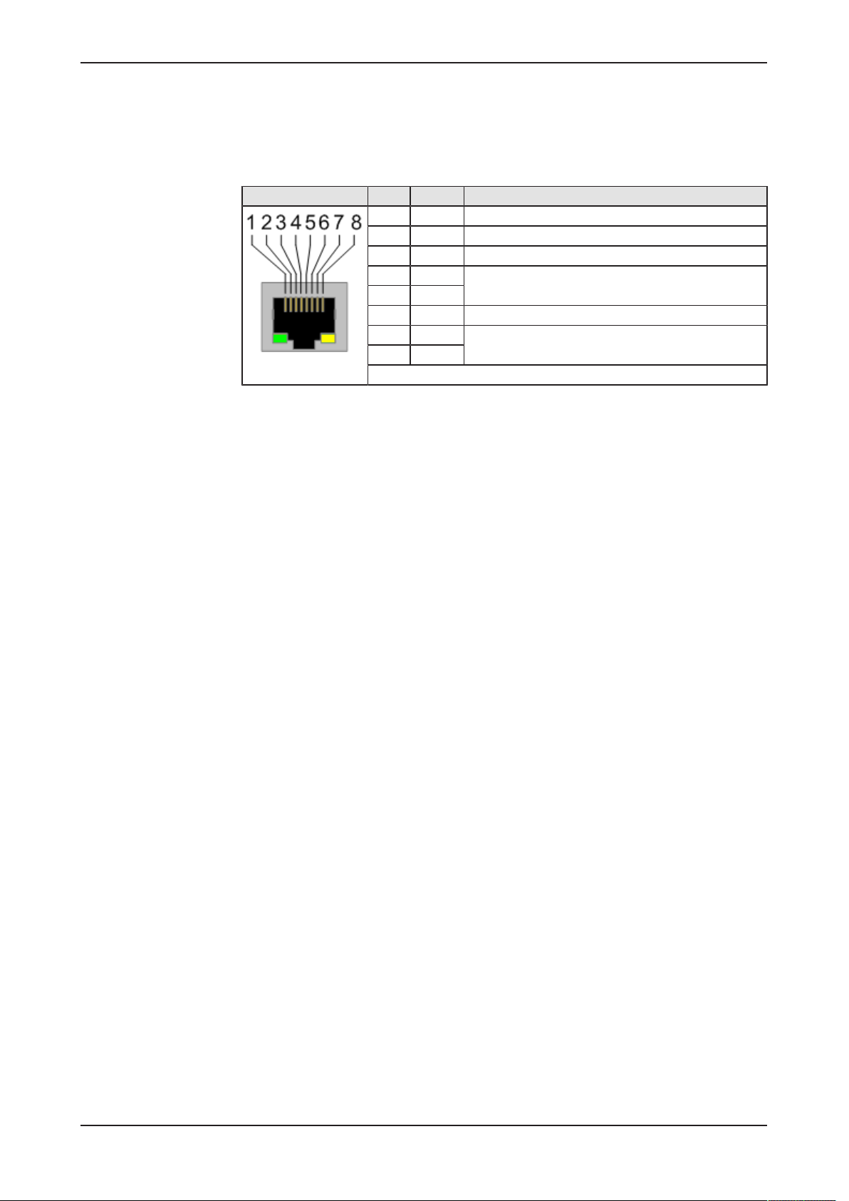
2.4.2 X500 – Ethernet connectors
Two RJ45 jack Ethernet connectors X500. For identifying the connectors on
the board, see position (20) for channel 0 and position (19) for channel 1 in
section Positions of interfaces and operating elements [}page12].
Ethernet Pin Signal Description
1 TX+ Transmit data positive
2 TX– Transmit data negative
3 RX+ Receive data positive
4 Term 1 Connected and terminated to FE via RC
5 Term 1
6 RX– Receive data negative
7 Term 2 Connected and terminated to FE via RC
8 Term 2
Table10: Ethernet RJ45 pin assignment
For a description of the LEDs of the Ethernet connector, see section
LEDs [}page33].
combination*
combination*
* Bob Smith Termination
NXHX 90-JTAG | Device description
DOC170202HW03EN | Revision 3 | English | 2019-01 | Released | Public
© Hilscher 2019

Descriptions and drawings 19/82
2.4.3 X600 – Host interface
Host interface connector X600. For identifying the connector on the board,
see position (22) in section Positions of interfaces and operating
elements [}page12].
The netX 90 offers many pin sharing options, which – for better overview –
are grouped into three tables:
· Host interface mode
– Parallel DPM
– Extension bus
– SDRAM
– Serial DPM
· MMIO and internal signals
– SQI
– I2C
– MPWM
– SPI
· Communication interfaces and digital I/O
– UART
– XC
– GPIO
– IO Link
– Ethernet
– PIO
– XM
– CAN
– MLED
Important:
The pinning of the X600 host interface was especially designed to fit
the different pinning layouts of the various host interface modules
offered by Hilscher, therefore some of the pins share the same
signals.
Connect at this interface only modules that are listed in section
Devices for host interface [}page35].
NXHX 90-JTAG | Device description
DOC170202HW03EN | Revision 3 | English | 2019-01 | Released | Public
© Hilscher 2019
Descriptions and drawings 20/82
Signal options according to host interface mode
X600 Connector
layout
Pin Signal
X600 netX 90 Standard
signal
1 – +3V3 – – – –
2 – GND – – – –
3 D5 HIF_A16 DPM_ALE EXT_A16 SD_CAS# –
4 F1 HIF_SDCLK DPM_SIRQ EXT_CS2# SD_CLK –
5 – GND – – – –
6 L3 RST_OUT# RST_OUT# – – –
7 M3 RST_IN# RST_IN# – – –
8 – n.c. – – – –
9 E8 MII1_COL – EXT_D2 SD_D2 –
10 E10 MII1_RXER – EXT_D0 SD_D0 –
11 F2 HIF_DIRQ# DPM_DIRQ EXT_CS1# – –
12 E3 HIF_RDY DPM_RDY EXT_RDY SD_CKE –
13 – GND – – – –
14 E2 HIF_RD# DPM_RD# EXT_RD# – –
15 – n.c. – – – –
16 E1 HIF_WR# DPM_WR# EXT_WR# SD_WE# –
17 E7 PHY0_LED_LI
NK_IN
18 E9 MII1_CRS – EXT_D1 SD_D1 –
19 D7 HIF_BHE# HIF_BHE# EXT_BHE# SD_DQM1 –
20 – GND – – – –
21 – n.c. – – – –
22 – n.c. – – – –
23 – n.c. – – – –
24 D8 HIF_CS# DPM_CS# EXT_CS0# SD_CS# –
25 – GND – – – –
26 – n.c. – – – –
27 – n.c. – – – –
28 – n.c. – – – –
29 D6 HIF_A17 DPM_WRH# EXT_A17 SD_DQM0 –
30 E4 MII0_CRS – EXT_D7 SD_D7 –
31 E5 MII0_COL – EXT_D6 SD_D6 –
32 F5 MII0_TXEN – EXT_D5 SD_D5 –
33 – GND – – – –
34 D4 HIF_A15 DPM_A15 EXT_A15 SD_RAS# –
Table11: Pin assignment of X600 according to HIF mode (1)
Signal options according to host interface mode
Parallel
DPM
– EXT_D3 SD_D3 –
Extension
bus
SDRAM Serial
DPM
NXHX 90-JTAG | Device description
DOC170202HW03EN | Revision 3 | English | 2019-01 | Released | Public
© Hilscher 2019
Descriptions and drawings 21/82
X600 Connector
layout
Pin Signal
X600 netX 90 Standard
signal
35 D3 HIF_A14 DPM_A14 EXT_A14 SD_BA1 –
36 D2 HIF_A13 DPM_A13 EXT_A13 SD_BA0 –
37 D1 HIF_A12 DPM_A12 EXT_A12 SD_A12 –
38 C1 HIF_A11 DPM_A11 EXT_A11 SD_A11 –
39 B2 HIF_A10 DPM_A10 EXT_A10 SD_A10 –
40 C2 HIF_A9 DPM_A9 EXT_A9 SD_A9 –
41 A3 HIF_A8 DPM_A8 EXT_A8 SD_A8 –
42 B3 HIF_A7 DPM_A7 EXT_A7 SD_A7 –
43 C3 HIF_A6 DPM_A6 EXT_A6 SD_A6 –
44 A4 HIF_A5 DPM_A5 EXT_A5 SD_A5 –
45 B4 HIF_A4 DPM_A4 EXT_A4 SD_A4 –
46 C4 HIF_A3 DPM_A3 EXT_A3 SD_A3 –
47 A5 HIF_A2 DPM_A2 EXT_A2 SD_A2 –
48 B5 HIF_A1 DPM_A1 EXT_A1 SD_A1 –
49 C5 HIF_A0 DPM_A0 EXT_A0 SD_A0 –
50 – GND – – – –
51 A6 HIF_D15 DPM_D15 – – DPM0_SQI_SIO3
52 B6 HIF_D14 DPM_D14 – – DPM0_SQI_SIO2
53 C6 HIF_D13 DPM_D13 – – DPM0_SPI_SIRQ
54 A7 HIF_D12 DPM_D12 – – DPM0_SPI_DIRQ
55 B7 HIF_D11 DPM_D11 – – DPM0_SPI_CLK
56 C7 HIF_D10 DPM_D10 – – DPM0_SPI_CS#
57 A8 HIF_D9 DPM_D9 – – DPM0_SPI_MOSI
58 B8 HIF_D8 DPM_D8 – – DPM0_SPI_MISO
59 C8 HIF_D7 DPM_D7 EXT_D15 SD_D15 DPM1_SQI_SIO3
60 A9 HIF_D6 DPM_D6 EXT_D14 SD_D14 DPM1_SQI_SIO2
61 B9 HIF_D5 DPM_D5 EXT_D13 SD_D13 DPM1_SPI_SIRQ
62 C9 HIF_D4 DPM_D4 EXT_D12 SD_D12 DPM1_SPI_DIRQ
63 A10 HIF_D3 DPM_D3 EXT_D11 SD_D11 DPM1_SPI_CLK
64 B10 HIF_D2 DPM_D2 EXT_D10 SD_D10 DPM1_SPI_CS#
65 C10 HIF_D1 DPM_D1 EXT_D9 SD_D9 DPM1_SPI_MOSI
66 B11 HIF_D0 DPM_D0 EXT_D8 SD_D8 DPM1_SPI_MISO
67 – +3V3 – – – –
68 E6 PHY1_LED_LIN
K_IN
Table12: Pin assignment of X600 according to HIF mode (2)
Signal options according to host interface mode
Parallel
DPM
– EXT_D4 SD_D4 –
Extension
bus
SDRAM Serial
DPM
NXHX 90-JTAG | Device description
DOC170202HW03EN | Revision 3 | English | 2019-01 | Released | Public
© Hilscher 2019

Descriptions and drawings 22/82
Signal options of MMIOs and internal interfaces
Pin Signal options: MMIOs and internal interfaces
X600 netX 90 MMIO SQI (APP CPU) I2C MPWM SPI
1 – – – – – –
2 – – – – – –
3 D5 – – I2C_APP_SCL – –
4 F1 – – – – –
5 – – – – – –
6 L3 – – – MPWM5 –
7 M3 – – – – –
8 – – – – – –
9 E8 – – – – –
10 E10 – – – – –
11 F2 MMIO17 SQI1_APP_SIO3 – – –
12 E3 – – – – –
13 – – – – – –
14 E2 MMIO16 SQI1_APP_SIO2 – – –
15 – – – – – –
16 E1 – – – – –
17 E7 – – – – –
18 E9 – – – – –
19 D7 – – – – –
20 – – – – – –
21 – – – – – –
22 – – – – – –
23 – – – – – –
24 D8 – – – – –
25 – – – – – –
26 – – – – – –
27 – – – – – –
28 – – – – – –
29 D6 – – I2C_APP_SDA – –
30 E4 – – – – –
31 E5 – – – – –
32 F5 – – – – –
33 – – – – – –
34 D4 – – – – SPI0_APP_MISO
Table13: Signal options of X600 pins – MMIO and internal interfaces (1)
NXHX 90-JTAG | Device description
DOC170202HW03EN | Revision 3 | English | 2019-01 | Released | Public
© Hilscher 2019

Descriptions and drawings 23/82
Pin Signal options: MMIOs and internal interfaces
X600 netX 90 MMIO SQI (APP CPU) I2C MPWM SPI
35 D3 – – – – SPI0_APP_MOSI
36 D2 – – – – SPI0_APP_CS0#
37 D1 – – – – SPI0_APP_CS1#
38 C1 – – – – SPI0_APP_CLK
39 B2 – – – – –
40 C2 – – – – –
41 A3 – – – – –
42 B3 – – – – –
43 C3 – – – – –
44 A4 – – – – –
45 B4 – – – – –
46 C4 – – – – –
47 A5 – – – – –
48 B5 – – – – –
49 C5 – – – – –
50 – – – – – –
51 A6 MMIO15 SQI1_APP_MOSI – – –
52 B6 MMIO14 SQI1_APP_MISO – – –
53 C6 MMIO13 SQI1_APP_CLK – – –
54 A7 MMIO12 SQI1_APP_CS0# – – –
55 B7 MMIO11 – – – –
56 C7 MMIO10 – – – –
57 A8 MMIO9 – – – –
58 B8 MMIO8 – – – –
59 C8 – – – – –
60 A9 – – – – –
61 B9 – SQI0_APP_SIO3 – – SPI2_APP_CS2#
62 C9 – SQI0_APP_SIO2 – – SPI2_APP_CS1#
63 A10 – SQI0_APP_CLK – – SPI2_APP_CLK
64 B10 – SQI0_APP_CS0# – – SPI2_APP_CS0#
65 C10 – SQI0_APP_MOSI – – SPI2_APP_MOSI
66 B11 – SQI0_APP_MISO – – SPI2_APP_MISO
67 – – – – – –
68 E6 – – – – –
Table14: Signal options of X600 pins – MMIO and internal interfaces (2)
NXHX 90-JTAG | Device description
DOC170202HW03EN | Revision 3 | English | 2019-01 | Released | Public
© Hilscher 2019

Descriptions and drawings 24/82
Signal options of communication interfaces and digital I/O
Pin Signal options: Communication interfaces and digital I/O
X600 netX90UART XC GPIO IO Link Ethernet PIO
(APP CPU)
1 – – – – – – – – – –
2 – – – – – – – – – –
3 D5 – – – – – – – – –
4 F1 UART_XPIC
_APP_RTS#
5 – – – – – – – – – –
6 L3 – – – IO_LINK7_
7 M3 – – – – – – – – –
8 – – – – – – – – – –
9 E8 – – – – – – XM1_I05 – –
10 E10 – – – – – – – – –
11 F2 UART_XPIC
_APP_CTS#
12 E3 UART_XPIC
_APP_RXD
13 – – – – – – – – – –
14 E2 UART_APP_
RTS#
15 – – – – – – – – – –
16 E1 UART_APP_
CTS#
17 E7 – – – – – – – – –
18 E9 – – – – – – – – –
19 D7 UART_APP_
RXD
20 – – – – – – – – – –
21 – – – – – – – – – –
22 – – – – – – – – – –
23 – – – – – – – – – –
24 D8 UART_APP_
TXD
25 – – – – – – – – – –
26 – – – – – – – – – –
27 – – – – – – – – – –
28 – – – – – – – – – –
29 D6 – – – – – – – – –
30 E4 – – – – ETH_B_CRS – – – –
31 E5 – – – – ETH_B_COL – XM0_I05 – –
32 F5 – – – – ETH_B_TXEN – XM0_I04 – –
33 – – – – – – – – – –
34 D4 – – – – – – – – –
XC_TRI
GGER0
– – – – – – – –
– – – ETH_RXCLK – – – –
– – – ETH_MDC – – – –
– – – ETH_MDIO – – – –
– – – ETH_RXER – – – –
– – – – – – – –
Table15: Signal options of X600 pins – communication interfaces and digital I/O (1)
– – – – – – –
– PIO_APP27 – – –
OUT
XM CAN MLED
NXHX 90-JTAG | Device description
DOC170202HW03EN | Revision 3 | English | 2019-01 | Released | Public
© Hilscher 2019

Descriptions and drawings 25/82
Pin Signal options: Communication interfaces and digital I/O
X600 netX90UART XC GPIO IO Link Ethernet PIO
(APP CPU)
35 D3 – – – – – – – – –
36 D2 – – – – ETH_TXCLK – – – –
37 D1 – – – – ETH_TXEN – – – –
38 C1 – – – – ETH_TXD3 – – – –
39 B2 – – GPIO7 – ETH_TXD2 – – – –
40 C2 – – GPIO6 – ETH_TXD1 – – – –
41 A3 – – GPIO5 – ETH_TXD0 – – – –
42 B3 – – GPIO4 IO_LINK1B
_WAKEUP
43 C3 – – GPIO3 IO_LINK1B
_OE
44 A4 – – GPIO2 IO_LINK1B
_OUT
45 B4 – – GPIO1 IO_LINK1B
_IN
46 C4 – – GPIO0 IO_LINK0B
_WAKEUP
47 A5 – – – IO_LINK0B
_OE
48 B5 – – – IO_LINK0B
_OUT
49 C5 UART_XPIC
_APP_TXD
50 – – – – – – – – – –
51 A6 – – – IO_LINK7_
52 B6 – – – IO_LINK6_
53 C6 – – – IO_LINK5_
54 A7 – – – IO_LINK4_
55 B7 – – – IO_LINK3_
56 C7 – – – IO_LINK2_
57 A8 – – – – – – – – MLED5
58 B8 – – – – – – – – MLED4
59 C8 – – – – – PIO_APP7 – CAN1_AP
60 A9 – – – – – PIO_APP6 – CAN1_AP
– – IO_LINK0B
_IN
WAKEUP
WAKEUP
WAKEUP
WAKEUP
WAKEUP
WAKEUP
Table16: Signal options of X600 pins – communication interfaces and digital I/O (2)
ETH_RXDV – – – –
ETH_RXD3 – – – –
ETH_RXD2 – – – –
ETH_RXD1 – – – –
ETH_RXD0 – – – –
ETH_CRS – – CAN0_AP
ETH_COL – – CAN0_AP
ETH_TXER – – – –
– – – – MLED1
– – – – MLED1
– – – – MLED9
– – – – MLED8
– – – – MLED7
– – – – MLED6
XM CAN MLED
–
P_TX
–
P_RX
1
0
–
P_TX
–
P_RX
NXHX 90-JTAG | Device description
DOC170202HW03EN | Revision 3 | English | 2019-01 | Released | Public
© Hilscher 2019
 Loading...