

Page 1

Design Guide
COM-C
Communication Module
Hilscher Gesellschaft für Systemautomation mbH
www.hilscher.com
DOC021001DG12EN | Revision 12 | English | 2011-06 | Released | Public
Page 2

Introduction 2/64
Table of Contents
1 Introduction.............................................................................................................................................4
1.1 About this Document......................................................................................................................4
1.2 List of Revisions .............................................................................................................................6
1.3 Technical Features.........................................................................................................................8
1.4 Legal Notes ..................................................................................................................................10
1.4.1 Copyright ......................................................................................................................................... 10
1.4.2 Important Notes............................................................................................................................... 10
1.4.3 Exclusion of Liability ........................................................................................................................ 11
1.4.4 Warranty.......................................................................................................................................... 11
1.4.5 Export Regulations .......................................................................................................................... 11
2 Type of COM-C Modules......................................................................................................................12
2.1 Mechanical Dimensions ...............................................................................................................13
2.1.1 Common Mechanical Dimensions for COM-C Modules .................................................................. 13
2.1.2 Mechanical Dimensions of COM-C Modules ................................................................................... 14
2.2 Type of Connector........................................................................................................................20
2.3 Mounting of COM-C Modules ......................................................................................................22
2.4 Designation of the COM-C...........................................................................................................28
2.5 Meaning of the Rotary Switch ......................................................................................................29
3 Host Interface .......................................................................................................................................30
3.1 COM Pinning of the System Bus Connector X1 ..........................................................................31
3.2 COM-CA-SCEB Pinning of the System Bus Connector X1.........................................................33
3.3 Signal Overview and Pinning of the Fieldbus Connector X2 on COM-CN ..................................35
3.3.1 Fieldbus Connector X2 for AS-Interface-Master.............................................................................. 35
3.3.2 Fieldbus Connector X2 for CANopen-Master/-Slave ....................................................................... 36
3.3.3 Fieldbus Connector X2 for DeviceNet-Master/-Slave ...................................................................... 37
3.3.4 Fieldbus Connector X2 for PROFIBUS-Master/-Slave .................................................................... 38
3.3.5 Fieldbus Connector X2 for Ethernet ................................................................................................ 39
3.3.6 Fieldbus Connector X2 for CC-Link-Slave....................................................................................... 40
3.4 Signals of the Host Interface........................................................................................................41
3.4.1 Power Supply of the COM-C Modules............................................................................................. 41
3.4.2 RESET Signal ................................................................................................................................. 41
3.4.3 The Dual-port Memory Bus of COM ................................................................................................ 41
3.4.4 Address Bus and Data Bus ............................................................................................................. 42
3.4.5 Dual-Port Memory Control Lines ..................................................................................................... 42
3.4.6 Interrupt Line to the Host System .................................................................................................... 43
3.4.7 Busy Line to the Host System.......................................................................................................... 43
3.4.8 Interfacing to the Dual-Port Memory of COM-C............................................................................... 43
3.4.9 Timing Diagram of COM-C .............................................................................................................. 44
3.4.10 Interfacing to the Dual-Port Memory for COM-CA-SCEB ................................................................ 46
3.4.11 Timing Diagram of COM-CA-SCEB................................................................................................. 46
3.5 Integration a COM-C Module into a Host System........................................................................47
4 LEDs ......................................................................................................................................................48
4.1 LEDs for COM Modules ...............................................................................................................49
4.1.1 Ethernet........................................................................................................................................... 49
4.1.2 EtherNet/IP Adapter (Slave) ............................................................................................................ 49
4.1.3 AS-Interface Master......................................................................................................................... 50
4.1.4 CANopen Master............................................................................................................................. 51
4.1.5 CANopen Slave............................................................................................................................... 51
4.1.6 CC Link Slave.................................................................................................................................. 52
4.1.7 DeviceNet Master............................................................................................................................ 53
4.1.8 DeviceNet Slave.............................................................................................................................. 53
4.1.9 InterBus Slave ................................................................................................................................. 54
4.1.10 PROFIBUS DP Master .................................................................................................................... 55
4.1.11 PROFIBUS DP Slave ...................................................................................................................... 55
4.1.12 SERCOS (optical)............................................................................................................................ 56
5 Device Address ....................................................................................................................................57
6 Diagnostic Interface.............................................................................................................................58
6.1 Diagnostic Interface RS232C.......................................................................................................58
COM-C | Communication Module
DOC021001DG12EN | Revision 12 | English | 2011-06 | Released | Public © Hilscher, 2002-2011
Page 3

Introduction 3/64
7 Technical Data......................................................................................................................................59
7.1 Product Tests ...............................................................................................................................61
8 Appendix...............................................................................................................................................63
8.1 List of Tables................................................................................................................................63
8.2 List of Figures...............................................................................................................................63
8.2.1 Contacts .......................................................................................................................................... 64
COM-C | Communication Module
DOC021001DG12EN | Revision 12 | English | 2011-06 | Released | Public © Hilscher, 2002-2011
Page 4

Introduction 4/64
1 Introduction
1.1 About this Document
All OEM piggyback Modules of Hilscher GmbH are called COM (Communication Modules). These
Modules provide a universal and easy to use fieldbus interface for integration on various host systems. Through the set of standard application interfaces and the same board dimensions in each
COM family it is easy to switch between the different fieldbus systems, e.g. PROFIBUS DP, InterBus, CANopen, DeviceNet or Ethernet by changing the Module.
This manual describes only the hardware part of the Modules. The general application interface is
common to all our COM Modules and CIF PC cards described in our Toolkit-Manual and the fieldbus related details are defined in our Protocol Interface Manuals.
COM-C | Communication Module
DOC021001DG12EN | Revision 12 | English | 2011-06 | Released | Public © Hilscher, 2002-2011
Page 5
Introduction 5/64
A new generation of communication Modules exists named COMX Modules and offer beside fieldbus communication also Real-Time Ethernet communication. The application interface is different
(not compatible) compared to COM Modules. The COMX Modules are described in an own manual
now. The following two tables give a comparison of both COM and COMX Modules.
Comparison COM and COMX Modules
Basic differences between COM-C and COMX-C
COM-C COMX-C
Processor EC1 netX
Host Interface 8 Bit 8 / 16 Bit
Dual-Port Memory size 2 KByte or 8 KByte 16 KByte
USB Interface No Yes
Table 1: Basic differences between COM and COMX
Comparison of supported protocols for COM-C and COMX-C
COM-C COMX-C
AS-Interface Master supported in preparation
CANopen Master supported supported
CANopen Slave supported supported
CC-Link Slave supported supported
CompoNet Slave - in preparation
DeviceNet Master supported supported
DeviceNet Slave supported supported
InterBus Slave supported not supported by netX technology
PROFIBUS DP Master supported supported
PROFIBUS DP Slave supported supported
SERCOS II supported not supported by netX technology
EtherCAT Master - supported
EtherCAT Slave - supported
EtherNet/IP Scanner (Master) - supported
EtherNet/IP Adapter (Slave) supported supported
Open Modbus/TCP supported supported
POWERLINK Controlled Node - supported
PROFINET IO RT Controller - supported
PROFINET IO RT Device - supported
SERCOS III Master - supported
SERCOS III Slave - supported
Table 2: Comparison of supported protocols for COM and COMX
COM-C | Communication Module
DOC021001DG12EN | Revision 12 | English | 2011-06 | Released | Public © Hilscher, 2002-2011
Page 6
Introduction 6/64
1.2 List of Revisions
Rev Date Name Revision
7 2009-10-01 H. Hentsch COMX-CA-DP, COMX-CN-DP, COMX-CA-CO, COMX-CN-CO, COMX-CA-CO,
COMX-CN-CO, COMX-CA-CCS and COMX-CN-CCS added
Chapter 1 restructured
Table
Basic differences between COM and COMX and Comparison of supported
protocols for COM and COMX added.
Figure Block Diagram of the COMX-C Modules and explaining text added
Section Mechanical Dimensions of COM-A Modules: M0400272 (update),
M0900141 (new)
Section Mechanical Dimensions of COM-B Modules: M0400282 (update),
M0900151 (new), M0400291 (kept)
Section
M0200373 (update), M0200463 (kept), M0300632 (update), M0400353 (update),
M0400363 (update), M0600172 (update), M0900161 (new)
Section
M0600121 (new), M0900102 (new), M0200402 (kept)
Section
Section : SYNC Signals added
Section Signal Overview and Pinning of the Fieldbus Connector X2 on COM-CN:
Added that Pin 21 is used for isolation
Section Timing Diagram of the COMX-C: Both tables updated and notes ex-
panded
Section LEDs divided into LEDs for COM and LEDs for COMX
Subsections in LEDs for COMX Modules updated respectively added
Section
8 2009-10-27 H. Hentsch Section Diagnostic Interface USB:: USB interface circuit modified
Temperature range for COMX Modules. -20 … 65°C
9 2009-11-11 H. Hentsch Section Fieldbus Connector X2 for Real-Time Ethernet:
- LED names changed to COM0 and COM1
- Figure 6 with example added
Section LEDs:
- Figure 14: Example how to connect the LEDs COMX-CN Fieldbus and
- Figure 15: Example how to connect the LEDs COMX-CN-RE added
Section LEDs for COMX Modules with references to signal COM0 and COM1 for
all Real-Time Ethernet protocols
Table 3: List of Revisions (Part 1)
Mechanical Dimensions of COM-C Modules:
Mounting of COM-C Modules: M0500081 (new), M0100084 (update),
Mounting of COM-C Modules expanded (4 bolt types)
Technical Data: New modules added
Continued on next page.
COM-C | Communication Module
DOC021001DG12EN | Revision 12 | English | 2011-06 | Released | Public © Hilscher, 2002-2011
Page 7
Introduction 7/64
Rev Date Name Revision
10 2010-07-13 H. Hentsch Table 2: Comparison of supported protocols for COM and COMX updated:
CANopen Slave, PROFIBUS DP Slave and DeviceNet Slave for COMX-C supported
Table 9: Available COMX-C Modules updated with COMX-C for Fieldbus Slaves
Table 7: Usage of Bolt for COM Modules updated
Designation of the COM-C expanded
Section Fieldbus Connector X2 for CANopen-Master/-Slave: COMX-CN-COS
added
Section
added
Section
added
Section
Section Fieldbus Connector X2 for PROFIBUS-Master/-Slave: Note 2 added
Section Diagnostic Interface USB: Note removed, because firmware now supports
USB
Table 74: Hardware Revision of COMX Modules with new USB Interface updated
Table 75: Hardware Revision of COMX Modules with old USB Interface updated
German text replaced by English text in the following drawings: M0500081,
M0500084, M0600121, M0900141, M0900151, M0400353
Section SERCOS III Slave, CANopen Slave, DeviceNet Slave and PROFIBUS
DP Slave added with LED Description
Table 38: Technical Data – Operating Condition: COMX-Cx-COS, COMX-Cx-DNS
and COMX-Cx-DPS added
11 2011-03-20 H. Hentsch Section Mechanical Dimensions of COM-C Modules:
M0200373 updated to M0200374, M0200463 updated to M0200464. Tolerance of
PCB thickness is 1.00 mm (-0,0 +0,2)
Section
12 2011-06-10 R. Göbel
H. Hentsch
Table 4: List of Revisions (Part 2)
Separation of documents for COM and COMX.
This manual contains the description for COM.
COM-A and COM-B removed as they are to be discontinued.
Section Mechanical Dimensions of COM-C Modules: Section updated, M0200374
updated, M0300632 updated
Table 5: COM-CA-EIS and COM-CN-EIS added
Section Meaning of the Rotary Switch added
Fieldbus Connector X2 for DeviceNet-Master/-Slave: COMX-CN-DNS
Fieldbus Connector X2 for PROFIBUS-Master/-Slave: COMX-CN-DPS
Fieldbus Connector X2 for CANopen-Master/-Slave: Note 2 added
Type of Connector: Headline ‘Cheaper version’ set to right position
COM-C | Communication Module
DOC021001DG12EN | Revision 12 | English | 2011-06 | Released | Public © Hilscher, 2002-2011
Page 8

Introduction 8/64
1.3 Technical Features
Common Technical Features for COM-C
Small footprint for the host connector with 50 mil grid
Solid mechanical assembly and a massive connection to earth ground by metal blocks spe-
cial design for the requirements of the Modules with fieldbus connector
Two dowels for exact mounting of the Module on the host board
Metal blocks can easily modified for special customer requirements
Front panel can be mounted on the metal blocks that the modules have always the same
front size and covers the fieldbus connector
Easy to use dual-port memory interface, with additional serial and diagnostic interface
Host interface is designed for 16 KByte address space of the dual-port memory with 8 bit bus
width.
3.3 V power supply reduce power consumption
Available in extended temperature specification
With the COM-C we have a much more compact form factor and additional technical features as
the already established COM Modules.
Extremely compact size 30 x 70 mm
Available with angled and without fieldbus connector
All fieldbus connectors are placed on one side, which is the edge side on the host board to
reserves space
2.5 mm space below the Module available for SMD components on the host board
Now you can have only one type of base board (for each COM family) on stock and you can mount
the requested fieldbus interface short before shipment to the customer. This gives much more
flexibility and saves money even if you have same mechanical constraints (for each COM family) in
comparison to our existing COM Modules. Therefore we have Modules with angled, straight and
without fieldbus connectors:
COM-CA COM-C Modules with angled fieldbus connector
COM-CN COM-C Modules without fieldbus connector
COM-C | Communication Module
DOC021001DG12EN | Revision 12 | English | 2011-06 | Released | Public © Hilscher, 2002-2011
Page 9
Introduction 9/64
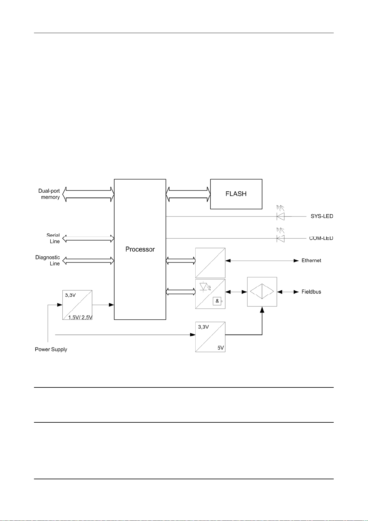
Description of COM Modules
All COM-C have a powerful processor and a complete fieldbus interface including isolated drivers
and the connector according to the standard. The slave modules have additional rotary switches to
set up the station address.
All boards require only a single stabilized 3.3 Voltage. All other voltages are created by DC/DC
converter on the COM-C Module.
The access to the COM-C Module is through the dual-port memory which can be easily integrated
as a static memory device. It has a non multiplexed 8 bit data bus with several control lines to the
host system. Between the COM-C Module and the host system it is possible to generate interrupts
for data handling.
Generally the firmware and the configuration data are stored permanently in FLASH memory by
loading the data through the dual port memory or the serial diagnostic line.
Figure 1: Block Diagram of the COM-C Modules
Note: The COM-CA-SCEB has only the special communication interface chip SERCON 816
on board. Programming of this chip must be done directly from the host application.
The description of the communication interface chip SERCON 816 can be get from the
‘SERCOS International’.
COM-C | Communication Module
DOC021001DG12EN | Revision 12 | English | 2011-06 | Released | Public © Hilscher, 2002-2011
Page 10

Introduction 10/64
1.4 Legal Notes
1.4.1 Copyright
© Hilscher, 2002-2011, Hilscher Gesellschaft für Systemautomation mbH
All rights reserved.
The images, photographs and texts in the accompanying material (user manual, accompanying
texts, documentation, etc.) are protected by German and international copyright law as well as international trade and protection provisions. You are not authorized to duplicate these in whole or in
part using technical or mechanical methods (printing, photocopying or other methods), to manipulate or transfer using electronic systems without prior written consent. You are not permitted to
make changes to copyright notices, markings, trademarks or ownership declarations. The included
diagrams do not take the patent situation into account. The company names and product descriptions included in this document may be trademarks or brands of the respective owners and may be
trademarked or patented. Any form of further use requires the explicit consent of the respective
rights owner.
1.4.2 Important Notes
The user manual, accompanying texts and the documentation were created for the use of the
products by qualified experts, however, errors cannot be ruled out. For this reason, no guarantee
can be made and neither juristic responsibility for erroneous information nor any liability can be assumed. Descriptions, accompanying texts and documentation included in the user manual do not
present a guarantee nor any information about proper use as stipulated in the contract or a warranted feature. It cannot be ruled out that the user manual, the accompanying texts and the documentation do not correspond exactly to the described features, standards or other data of the delivered product. No warranty or guarantee regarding the correctness or accuracy of the information
is assumed.
We reserve the right to change our products and their specification as well as related user manuals, accompanying texts and documentation at all times and without advance notice, without obligation to report the change. Changes will be included in future manuals and do not constitute any
obligations. There is no entitlement to revisions of delivered documents. The manual delivered with
the product applies.
Hilscher Gesellschaft für Systemautomation mbH is not liable under any circumstances for direct,
indirect, incidental or follow-on damage or loss of earnings resulting from the use of the information
contained in this publication.
COM-C | Communication Module
DOC021001DG12EN | Revision 12 | English | 2011-06 | Released | Public © Hilscher, 2002-2011
Page 11

Introduction 11/64
1.4.3 Exclusion of Liability
The software was produced and tested with utmost care by Hilscher Gesellschaft für Systemautomation mbH and is made available as is. No warranty can be assumed for the performance and
flawlessness of the software for all usage conditions and cases and for the results produced when
utilized by the user. Liability for any damages that may result from the use of the hardware or software or related documents, is limited to cases of intent or grossly negligent violation of significant
contractual obligations. Indemnity claims for the violation of significant contractual obligations are
limited to damages that are foreseeable and typical for this type of contract.
It is strictly prohibited to use the software in the following areas:
for military purposes or in weapon systems;
for the design, construction, maintenance or operation of nuclear facilities;
in air traffic control systems, air traffic or air traffic communication systems;
in life support systems;
in systems in which failures in the software could lead to personal injury or injuries leading to
death.
We inform you that the software was not developed for use in dangerous environments requiring
fail-proof control mechanisms. Use of the software in such an environment occurs at your own risk.
No liability is assumed for damages or losses due to unauthorized use.
1.4.4 Warranty
Although the hardware and software was developed with utmost care and tested intensively, Hilscher Gesellschaft für Systemautomation mbH does not guarantee its suitability for any purpose
not confirmed in writing. It cannot be guaranteed that the hardware and software will meet your requirements, that the use of the software operates without interruption and that the software is free
of errors. No guarantee is made regarding infringements, violations of patents, rights of ownership
or the freedom from interference by third parties. No additional guarantees or assurances are
made regarding marketability, freedom of defect of title, integration or usability for certain purposes
unless they are required in accordance with the law and cannot be limited. Warranty claims are
limited to the right to claim rectification.
1.4.5 Export Regulations
The delivered product (including the technical data) is subject to export or import laws as well as
the associated regulations of different counters, in particular those of Germany and the USA. The
software may not be exported to countries where this is prohibited by the United States Export
Administration Act and its additional provisions. You are obligated to comply with the regulations at
your personal responsibility. We wish to inform you that you may require permission from state authorities to export, re-export or import the product.
COM-C | Communication Module
DOC021001DG12EN | Revision 12 | English | 2011-06 | Released | Public © Hilscher, 2002-2011
Page 12
Type of COM-C Modules 12/64
2 Type of COM-C Modules
The following table shows an overview about the availability of the different COM-C Modules.
Module Fieldbus / Protocol Type Connector
COM-CA-ASM AS-Interface Master angled
COM-CA-COS CANopen Slave angled
COM-CA-COM CANopen Master angled
COM-CA-CCS CC-Link Slave angled
COM-CA-DNS DeviceNet Slave angled
COM-CA-DNM DeviceNet Master angled
COM-CA-EN Ethernet angled
COM-CA-EIS EtherNet/IP Slave angled
COM-CA-IBS INTERBUS Slave angled
COM-CA-DPS PROFIBUS DP Slave angled
COM-CA-DPM PROFIBUS DP Master angled
COM-CA-SCEB SERCOS angled
COM-CN-ASM AS-Interface Master No
COM-CN-COS CANopen Slave No
COM-CN-COM CANopen Master No
COM-CN-CCS CC-Link Slave No
COM-CN-DNS DeviceNet Slave No
COM-CN-DNM DeviceNet Master No
COM-CN-EN Ethernet No
COM-CN-EIS EtherNet/IP Slave No
COM-CN-DPS PROFIBUS DP Slave No
COM-CN-DPS\NR
(NR = No Rotary switch)
COM-CN-DPM PROFIBUS DP Master No
Table 5: Available COM-C Modules
PROFIBUS DP Slave No
COM-C | Communication Module
DOC021001DG12EN | Revision 12 | English | 2011-06 | Released | Public © Hilscher, 2002-2011
Page 13

Type of COM-C Modules 13/64
2.1 Mechanical Dimensions
2.1.1 Common Mechanical Dimensions for COM-C Modules
After mounting the COM-CA Module parallel at a basis board the rotary switches, LEDs and the
fieldbus connector are on the top side and are angled to the basis board. The edge of all front elements are in one layer which is 2.5 mm ahead of the edge of printed circuit board of the COM
Module.
The COM-CN Module has to be used if the mechanical dimensions or order of the LEDs, switches
and fieldbus connector doesn't fit. In that case you have to place these components directly on the
motherboard and feed the signals to the connector X2 of the COM-CN Module.
Note Please take care on the isolation distance, because the optical isolation interface is on
the Module!
Especially for 12 MBit PROFIBUS the distance should as be less as possible.
For Ethernet, the signal traces should run parallel and should have the same length.
Please refer at the fieldbus standards for further information!
COM-C | Communication Module
DOC021001DG12EN | Revision 12 | English | 2011-06 | Released | Public © Hilscher, 2002-2011
Page 14

Type of COM-C Modules 14/64
2.1.2 Mechanical Dimensions of COM-C Modules
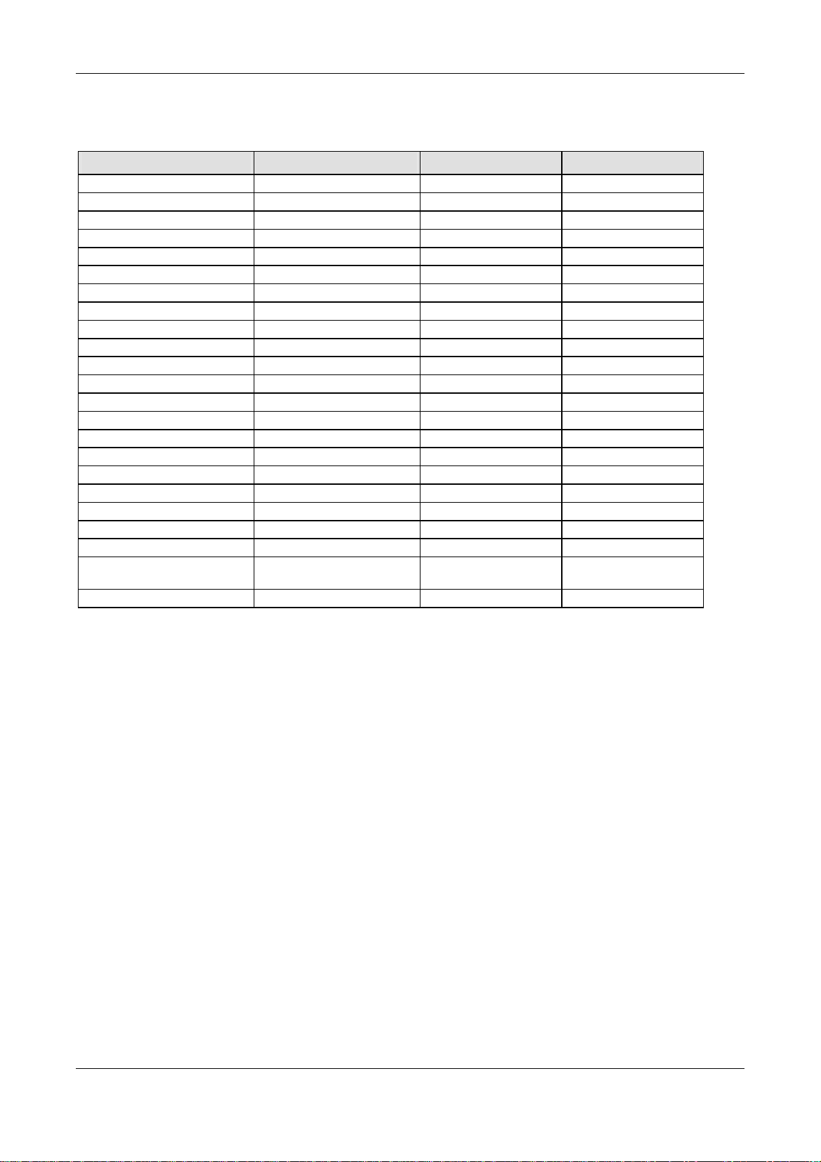
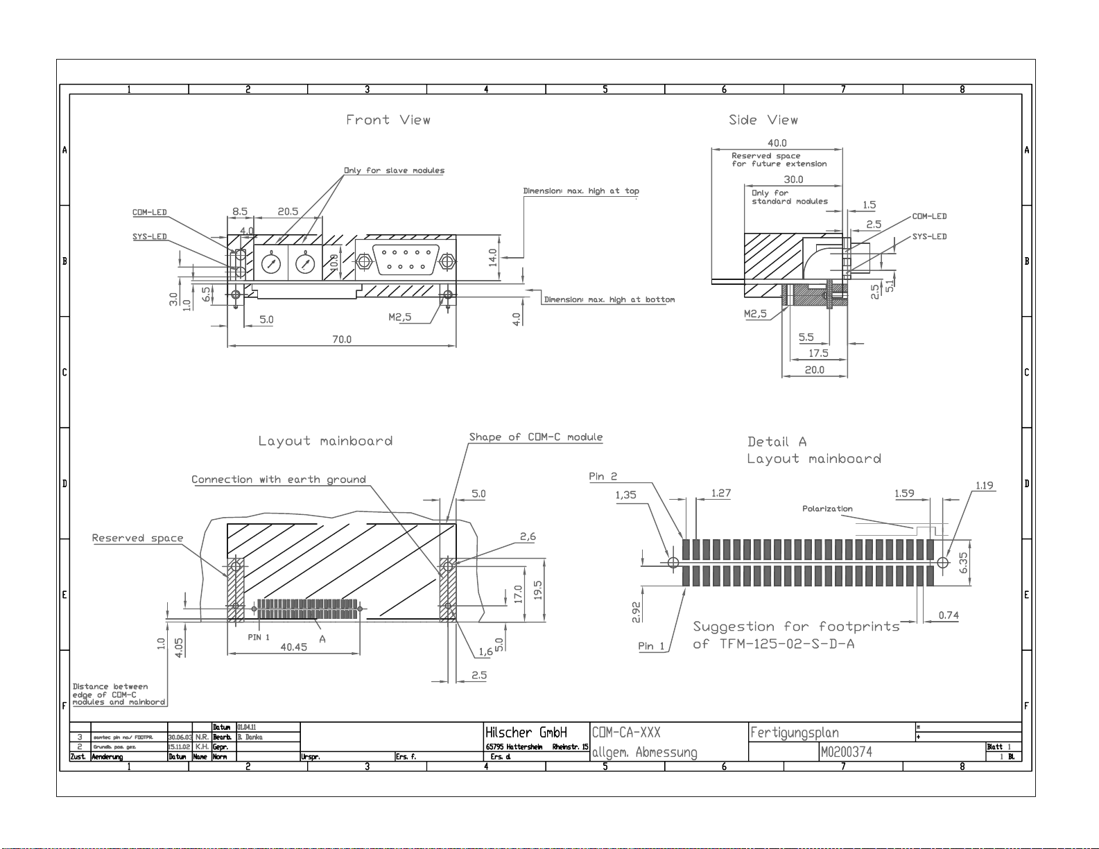
The COM-C Module has a board size of 30 x 70 mm. The maximum height of the components at
the top side of the printed circuit board is 14.0 mm including the fieldbus connector. Keep the
space of 14.0 mm above the top side free.
At the bottom side the maximum height is 4.0 mm, therefore you have 2.5 mm space for components on the host board below the Module. The power dissipation in that area should be less than
330 maw!
For further Module development please reserve additional 10 mm space behind the Module. There
are a few larger fieldbus interfaces which do not fit on the small board space. In that case a second
printed circuit board will be mounted on top of the Module and the 10 mm space is necessary for
the connection with flex stripe between these boards.
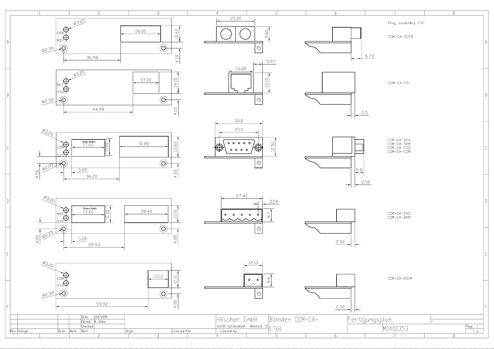
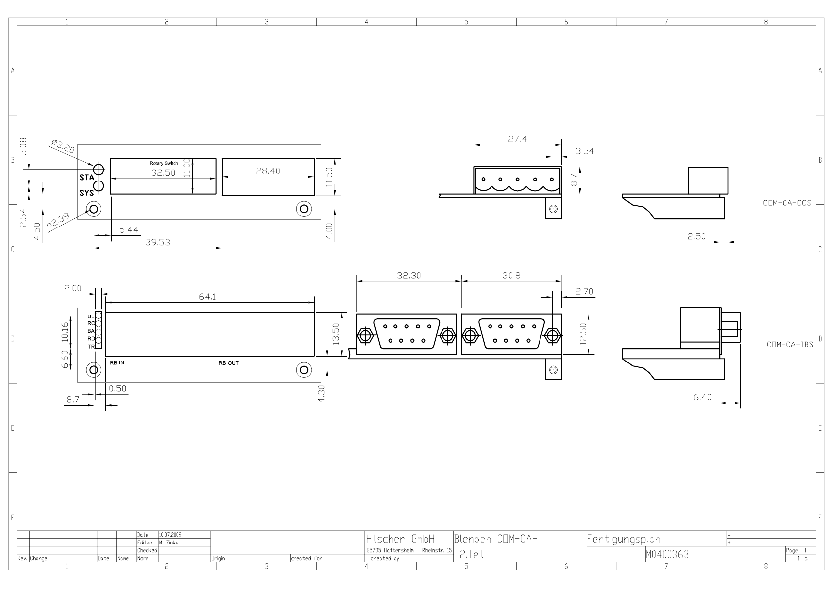
The general dimensions of the COM-C Modules are shown on the following drawings:
M0200374 General Mechanical dimension of COM-CA-XXX
M0200464 Mechanical dimension of COM-CN-XXX
M0300632 Mechanical dimension of light pipe of COM-CA-XXX
M0400353 Mechanical dimension of Front Plate and Connector of COM-CA-XXX (part 1)
M0400363 Mechanical dimension of Front Plate and Connector of COM-CA-XXX (part 2)
COM-C | Communication Module
DOC021001DG12EN | Revision 12 | English | 2011-06 | Released | Public © Hilscher, 2002-2011
Page 15
Page 16
Page 17
Page 18
Page 19
Page 20
Type of COM-C Modules 20/64
2.2 Type of Connector
The connector X1 for the host interface is a 50 pins SMT female type with a grid of 1.27 mm. The
COM-CN Modules have an additional fieldbus connector X2 with 30 pins of the same family.
The connector of the motherboard is the corresponding male type and can be ordered as follows:
In Germany FJH die Steckverbinder GmbH
Hinter dem Turm 7
D-55286 Wörrstadt
Germany
Tel. +49 (0) 67 32 / 93 27 -0
Fax +49 (0) 67 32 / 93 27 -27
Web: www.fjh.de
Email:
info@fjh.de
50 pin. Box header 127 KA - 050 SB
30 pin. Box header 127 KA - 030 SB
World Wide SAMTEC
www.samtec.com
Cheaper version
50 pin. Connector TFM - 125 - 02 - S - D – A TFC - 125 - 02 - F - D – A
30 pin. Connector TFM - 115 - 02 - S - D – A TFC - 115 - 02 - F - D – A
Note: Datasheet of SAMTEC TFM connector see next page!
Please notice that the polarization of X1 and X2 is opposite to Pin 1!
The fieldbus connector on the Module is defined by the fieldbus standard as followed:
Fieldbus Connector Vendor
AS-Interface 2 pin, COMBICON, male
Grid 5.08 mm
CANopen 9 pin, DSub, male div. Vendor
DeviceNet 5 pin, COMBICON, male
Grid 5.08 mm
Ethernet 8 pin, RJ45, female div. Vendor
PROFIBUS 9 pin, DSub, female div. Vendor
InterBus 9 pin, DSub, male, female div. Vendor
CC-Link 5 pin, COMBICON, male
Grid 5.08 mm
Table 6: Connector Types
ie. PHOENIX Contact
MSTBA2,5/2-5,08-G
ie. PHOENIX Contact
MSTBA2,5/5-5,08G-AU
ie. PHOENIX Contact
MSTBA2,5/5-G-AU
Please use the same type of connector at the motherboard if you have chosen the COM-CN Module.
COM-C | Communication Module
DOC021001DG12EN | Revision 12 | English | 2011-06 | Released | Public © Hilscher, 2002-2011
Page 21

Page 22

Type of COM-C Modules 22/64
2.3 Mounting of COM-C Modules
The COM-C Module has two metal blocks for mounting. This guaranties a robust mechanical construction and a solid connection to earth ground for the fieldbus connector. The metal blocks define
also the distance between the Module and host board. They are connected together with M2.5
screws.
On the front side of the metal blocks there are a M2.5 thread to mount a front panel directly on the
Module. This allows to have the same cutting in the device housing for all types of Modules.
Use fine technology that means six-mil-wide (150 μm) tracks
Note With this you have the possibility to get out between the pads.
For the power tracks you can insert a via straight in the pad.
To prevent a soldering problem please use a fine via (drill 0,2 mm).
Place a via between board edge and connector pad
Note There is 1 mm space between the connector and the board edge, where you can place
a 'normal' via (drill 0,3 mm) to feed the signals to the bottom side.
Figure 2: How to layout the Signals at the Connectors X1 and X2
COM-C | Communication Module
DOC021001DG12EN | Revision 12 | English | 2011-06 | Released | Public © Hilscher, 2002-2011
Page 23

Type of COM-C Modules 23/64
Four types of metal bolts are used. The following table lists the usage for each COM Module.
COM Type Left Side Right Side
COM-CA AS, CCS, CO, DN, DP, EN, IBS, SCEB COM-CA-B20X5 COM-CA-B20X5
COM-CN AS, CCS, CO, DN, DP, EN, IBS COM-CA-B20X5 COM-CA-B20X5
Table 7: Usage of Bolt for COM Modules
The drawings for the bolts are shown on the following drawings:
M0100084 Mechanical dimension of Bolt COM-CA-B20X5
M0600121 Mechanical dimension of Bolt COM-CA-B31,5X5
M0900102 Mechanical dimension of Bolt COM-CA-B24X5
M0200402 Mechanical dimension how to assemble COM-CA-XXX on the mother board
COM-C | Communication Module
DOC021001DG12EN | Revision 12 | English | 2011-06 | Released | Public © Hilscher, 2002-2011
Page 24

Page 25

Page 26

Page 27

Page 28

Type of COM-C Modules 28/64
2.4 Designation of the COM-C
Each COM-C Module has a matrix code label. A matrix label contains 3 items:
1. Part number
2. Hardware Revision
3. Serial number
The figure shows part number 1521.416, hardware revision 3 and serial number 00200.
Figure 3: Example Matrix Code label of COM-C Modules
The label is normally glued on top of the main processor.
COM-C | Communication Module
DOC021001DG12EN | Revision 12 | English | 2011-06 | Released | Public © Hilscher, 2002-2011
Page 29

Type of COM-C Modules 29/64
2.5 Meaning of the Rotary Switch
The following figure shows the meaning of the rotary switch for COM-CA-DPS, COM-CA-COS and
COM-CA-DNS. The rotary switches are to set the bus address.
Figure 4: Meaning of the Rotary Switch
The following figure shows the meaning of the rotary switch for COM-CA-CCS and COM-CN-CCS.
The left and the middle rotary switch are to set the bus address.
Figure 5: Meaning of the Rotary Switch of COM-Cx-CCS
COM-C | Communication Module
DOC021001DG12EN | Revision 12 | English | 2011-06 | Released | Public © Hilscher, 2002-2011
Page 30

Host Interface 30/64
3 Host Interface
Attention! All COM modules have an operation voltage of 3.3 V which reduces the power con-
sumption. Therefore the voltage levels of the signals have to be not higher than 3.3 V
otherwise the module will be damaged.
The next sections show an overview of the signal pinning of the system connector.
COM-C | Communication Module
DOC021001DG12EN | Revision 12 | English | 2011-06 | Released | Public © Hilscher, 2002-2011
Page 31

Host Interface 31/64
3.1 COM Pinning of the System Bus Connector X1
Pin Signal Symbol Type
1 Word Interface, active low WIF# GND if D8 - D15 is available (16 bit),
left unconnected if not (8 bit)
2 Bus high enable (future use), active low BHE# LVTTL Input
3 Data line 15 (future use) D15 LVTTL Input / Output
4 Data line 14 (future use) D14 LVTTL Input / Output
5 Data line 13 (future use) D13 LVTTL Input / Output
6 Data line 12 (future use) D12 LVTTL Input / Output
7 Data line 11 (future use) D11 LVTTL Input / Output
8 Data line 10 (future use) D10 LVTTL Input / Output
9 Data line 9 (future use) D9 LVTTL Input / Output
10 Data line 8 (future use) D8 LVTTL Input / Output
11 Ground GND
12 Power Supply +3.3 V
13 Transmit Data, Serial line TXD1 LVTTL Output
14 Receive Data, Serial line RXD1 LVTTL Input
15 Request to Send, Serial line RTS1 LVTTL Output
16 Clear to Send, Serial line CTS1 LVTTL Input
17 reserved for future - don't connect -
18 reserved for future - don't connect -
19 Receive Data, Diagnostic line RX0 LVTTL Input
20 Transmit Data, Diagnostic line TX0 LVTTL Output
21 Reset, active low RES# LVTTL Input; 10 k pull up
22 Busy, active low BUSY# LVTTL Output
23 Interrupt, active low INT# LVTTL Output
24 Read, active low RD# LVTTL Input
25 Write, active low WR# LVTTL Input
26 Chip select, active low CS# LVTTL Input
27 Address line 13 A13 LVTTL Input
28 Address line 12 A12 LVTTL Input
29 Address line 11 A11 LVTTL Input
30 Address line 10 A10 LVTTL Input
31 Address line 9 A9 LVTTL Input
32 Address line 8 A8 LVTTL Input
33 Address line 7 A7 LVTTL Input
34 Address line 6 A6 LVTTL Input
35 Address line 5 A5 LVTTL Input
36 Address line 4 A4 LVTTL Input
37 Address line 3 A3 LVTTL Input
38 Address line 2 A2 LVTTL Input
39 Address line 1 A1 LVTTL Input
40 Address line 0 A0 LVTTL Input
Table 8: COM Pinning of the System Bus Connector X1 (Part 1)
Continued on next page.
COM-C | Communication Module
DOC021001DG12EN | Revision 12 | English | 2011-06 | Released | Public © Hilscher, 2002-2011
Page 32

Host Interface 32/64
Pin Signal Symbol Type
41 Data line 7 D7 LVTTL Input / Output
42 Data line 6 D6 LVTTL Input / Output
43 Data line 5 D5 LVTTL Input / Output
44 Data line 4 D4 LVTTL Input / Output
45 Data line 3 D3 LVTTL Input / Output
46 Data line 2 D2 LVTTL Input / Output
47 Data line 1 D1 LVTTL Input / Output
48 Data line 0 D0 LVTTL Input / Output
49 Ground GND
50 Power Supply +3.3 V
Table 9: COM Pinning of the System Bus Connector X1 (Part 2)
COM-C | Communication Module
DOC021001DG12EN | Revision 12 | English | 2011-06 | Released | Public © Hilscher, 2002-2011
Page 33

Host Interface 33/64
3.2 COM-CA-SCEB Pinning of the System Bus Connector X1
Pin Signal Symbol Type
1 Word Interface, active low WIF# GND if D8 - D15 is available (16 bit),
left unconnected if not (8 bit)
2 Bus high enable, active low BHE# LVTTL Input
3 Data line 15 D15 LVTTL Input / Output
4 Data line 14 D14 LVTTL Input / Output
5 Data line 13 D13 LVTTL Input / Output
6 Data line 12 D12 LVTTL Input / Output
7 Data line 11 D11 LVTTL Input / Output
8 Data line 10 D10 LVTTL Input / Output
9 Data line 9 D9 LVTTL Input / Output
10 Data line 8 D8 LVTTL Input / Output
11 Ground GND
12 Power Supply +3.3 V
13 reserved for future - don't connect -
14 reserved for future - don't connect -
15 reserved for future - don't connect -
16 reserved for future - don't connect -
17 Interrupt, active low INT1# LVTTL Output
18 reserved for future - don't connect -
19 reserved for future - don't connect -
20 reserved for future - don't connect -
21 Reset, active low RES# LVTTL Input; 10 k … 30 k pull up
22 Busy, active low BUSY# LVTTL Output
23 Interrupt, active low INT0# LVTTL Output
24 Read, active low RD# LVTTL Input
25 Write, active low WR# LVTTL Input
26 Chip select, active low CS# LVTTL Input
27 Address line 13 (reserved for future use) A13 LVTTL Input
28 Address line 12 A12 LVTTL Input
29 Address line 11 A11 LVTTL Input
30 Address line 10 A10 LVTTL Input
31 Address line 9 A9 LVTTL Input
32 Address line 8 A8 LVTTL Input
33 Address line 7 A7 LVTTL Input
34 Address line 6 A6 LVTTL Input
35 Address line 5 A5 LVTTL Input
36 Address line 4 A4 LVTTL Input
37 Address line 3 A3 LVTTL Input
38 Address line 2 A2 LVTTL Input
39 Address line 1 A1 LVTTL Input
40 Address line 0 A0 LVTTL Input
Table 10: COM-CA-SCEB Pinning of the System Bus Connector X1 (Part 1)
Continued on next page.
COM-C | Communication Module
DOC021001DG12EN | Revision 12 | English | 2011-06 | Released | Public © Hilscher, 2002-2011
Page 34

Host Interface 34/64
Pin Signal Symbol Type
41 Data line 7 D7 LVTTL Input / Output
42 Data line 6 D6 LVTTL Input / Output
43 Data line 5 D5 LVTTL Input / Output
44 Data line 4 D4 LVTTL Input / Output
45 Data line 3 D3 LVTTL Input / Output
46 Data line 2 D2 LVTTL Input / Output
47 Data line 1 D1 LVTTL Input / Output
48 Data line 0 D0 LVTTL Input / Output
49 Ground GND
50 Power Supply +3.3 V
Table 11: COM-CA-SCEB Pinning of the System Bus Connector X1 (Part 2)
COM-C | Communication Module
DOC021001DG12EN | Revision 12 | English | 2011-06 | Released | Public © Hilscher, 2002-2011
Page 35

Host Interface 35/64
3.3 Signal Overview and Pinning of the Fieldbus Connector X2 on COM-CN
3.3.1 Fieldbus Connector X2 for AS-Interface-Master
Fieldbus connector X2 for COM-CN-ASM
Pin Signal Symbol Type Pin at Fieldbus
Connector
COMBICON
2pin
1
2
3
4
5
6
7
8
9
10 AS-i, Receive Data ASI_RX
11 AS-i, Power Fail ASI_PF LVTTL Output Note 1
12 AS-i, Transmit Data ASI_TX LVTTL Output Note 1
13 COM-LED, STA, Cathode yellow LED STA# 4 mA Output
14 SYS-LED, RUN, Cathode green LED RUN# 4 mA Output
15 COM-LED, ERR, Cathode red LED ERR# 4 mA Output
16 SYS-LED, RDY, Cathode yellow LED RDY# 4 mA Output
17 Ground GND
18 Power Supply +3.3 V
19 Peripheral IO PIO LVTTL Input / Output
20 Don't use - needed for isolation
21 Don't use - needed for isolation
22
23
24
25
26
27
28
29 AS-i + Bus line AS-i+ +24 V with AS-i 1
30 AS-i - Bus line AS-i- 0 V with AS-i 2
Table 12: Fieldbus Connector X2 for AS-Interface-Master
LVTTL Input Note 1
Note Information
1 LVTTL Signals could be only used without the hardware interface on the COM. Ask for special customer ver-
sion.
Table 13: Notes for Fieldbus Connector X2 for AS-Interface-Master
COM-C | Communication Module
DOC021001DG12EN | Revision 12 | English | 2011-06 | Released | Public © Hilscher, 2002-2011
Page 36

Host Interface 36/64
3.3.2 Fieldbus Connector X2 for CANopen-Master/-Slave
Fieldbus connector X2 for COM-CN-COM / COM-CN-COS
Pin Signal Symbol Type Pin at Fieldbus
Connector
DSub 9, male
1
2
3
4
5
6
7 CAN, Receive Data CAN_RX1 LVTTL Input Note 1
8
9 CAN, Transmit Data CAN_TX1 LVTTL Output Note 1
10
11
12
13 COM-LED, STA, Cathode yellow LED STA# 4 mA Output Note 2
14 SYS-LED, RUN, Cathode green LED RUN# 4 mA Output
15 COM-LED, ERR, Cathode red LED ERR# 4 mA Output
16 SYS-LED, RDY, Cathode yellow LED RDY# 4 mA Output
17 Ground GND
18 Power Supply +3.3 V
19 Peripheral IO PIO LVTTL Input / Output
20 Don't use - needed for isolation
21 Don't use - needed for isolation
22
23 CAN_H Bus line CAN_H ISO 11898 7
24
25
26 CAN Ground CAN_GND 3
27
28
29 CAN_L Bus line CAN_L ISO 11898 2
30
Table 14: Fieldbus Connector X2 for CANopen-Master/-Slave
Note Information
1 LVTTL Signals could be only used without the hardware interface on the COM. Ask for special customer ver-
sion.
2 Yellow LED for COM-CN-COM / COM-CN-COS
Table 15: Notes for Fieldbus Connector X2 for CANopen-Master/-Slave
COM-C | Communication Module
DOC021001DG12EN | Revision 12 | English | 2011-06 | Released | Public © Hilscher, 2002-2011
Page 37

Host Interface 37/64
3.3.3 Fieldbus Connector X2 for DeviceNet-Master/-Slave
Fieldbus connector X2 for COM-CN-DNM / COM-CN-DNS
Pin Signal Symbol Type Pin at Fieldbus
connector
COMBICON
5pin
1
2
3
4
5
6
7 CAN, Receive Data CAN_RX1 LVTTL Input Note 1
8
9 CAN, Transmit Data CAN_TX1 LVTTL Output Note 1
10
11 CAN, Power Fail CAN_PF1 LVTTL Input Note 1
12
13 MNS-LED, active low, Cathode green LED MNS_CG# 4 mA Output
14 RUN-LED, RUN, Cathode green LED RUN# 4 mA Output
15 MNS-LED, active low, Cathode red LED MNS_CR# 4 mA Output
16 SYS-LED, RDY, Cathode yellow LED RDY# 4 mA Output
17 Ground GND
18 Power Supply +3.3 V
19 Peripheral IO PIO LVTTL Input / Output
20 Don't use - needed for isolation
21 Don't use - needed for isolation
22
23
24
25
26 Reference potential DeviceNet V- 1
27 CAN Low-Signal CAN_L 2
28 Shield Drain 3
29 CAN High-Signal CAN_H 4
30 +24V Power Supply DeviceNet V+ 5
Table 16: Fieldbus Connector X2 for DeviceNet-Master/-Slave
Note Information
1 LVTTL Signals could be only used without the hardware interface on the COM. Ask for special customer ver-
sion.
Table 17: Notes for Fieldbus Connector X2 for DeviceNet-Master/-Slave
COM-C | Communication Module
DOC021001DG12EN | Revision 12 | English | 2011-06 | Released | Public © Hilscher, 2002-2011
Page 38

Host Interface 38/64
3.3.4 Fieldbus Connector X2 for PROFIBUS-Master/-Slave
Fieldbus connector X2 for COM-CN-DPM / COM-CN-DPS
Pin Signal Symbol Type Pin at Fieldbus
connector
DSub-9,
female
1 PROFIBUS, Receive Data PB_RX LVTTL Input Note 1
2
3 PROFIBUS, Transmit Data PB_TX LVTTL Output Note 1
4
5 PROFIBUS, Enable Bus Driver PB_ENB LVTTL Output Note 1
6
7
8
9
10
11
12
13 COM-LED, STA, Cathode yellow LED STA# 4 mA Output Note 2
14 SYS-LED, RUN, Cathode green LED RUN# 4 mA Output
15 COM-LED, ERR, Cathode red LED ERR# 4 mA Output
16 SYS-LED, RDY, Cathode yellow LED RDY# 4 mA Output
17 Ground GND
18 Power Supply +3.3 V
19 Peripheral IO PIO LVTTL Input / Output
20 Don't use - needed for isolation
21 Don't use - needed for isolation
22 Reference potential DGND 5
23 Control CNTR-P LVTTL 4
24
25 Receive / Send Data-N RXD/TXD-N RS 485 8
26 Receive / Send Data-P RXD/TXD-P RS 485 3
27
28
29 Positive power supply VP + 5V 6
30
Table 18: Fieldbus Connector X2 for PROFIBUS-Master/-Slave
Note Information
1 LVTTL Signals could be only used without the hardware interface on the COM. Ask for special customer ver-
sion.
2 Yellow LED for COM-CN-DPM / COM-CN-DPS
Table 19: Notes for Fieldbus Connector X2 for PROFIBUS-Master/-Slave
COM-C | Communication Module
DOC021001DG12EN | Revision 12 | English | 2011-06 | Released | Public © Hilscher, 2002-2011
Page 39

Host Interface 39/64
3.3.5 Fieldbus Connector X2 for Ethernet
Fieldbus connector X2 for COM-CN-EN
Pin Signal Symbol Type Pin at Fieldbus
connector
RJ45
1
2 Ethernet, Receive Data N EN_IN MAC Input neg. Note 1
3
4 Ethernet, Receive Data P EN_IP MAC Input pos. Note 1
5
6 Ethernet , Transmit Data N EN_ON MAC Output neg. Note 1
7
8 Ethernet, Transmit Data P EN_OP MAC Output pos. Note 1
9
10
11
12
13 LINK-LED, active low LNK# 4 mA Output
14 SYS-LED, RUN, Cathode green LED RUN# 4 mA Output
15 ERR-LED, active low ERR# 4 mA Output
16 SYS-LED, RDY, Cathode yellow LED RDY# 4 mA Output
17 Ground GND
18 Power Supply +3.3 V
19 Peripheral IO PIO LVTTL Input / Output
20 Don't use - needed for isolation
21 Don't use - needed for isolation
22
23 Transmit Data + TX+ 1
24 Transmit Data - TX- 2
25 Receive Data + RX+ 3
26
27
28 Receive Data - RX- 6
29
30
Table 20: Fieldbus Connector X2 for Ethernet
Note Information
1 Ethernet Signals could be only used without the hardware interface on the COM. Ask for special customer ver-
sion.
Table 21: Notes for Fieldbus Connector X2 for Ethernet
COM-C | Communication Module
DOC021001DG12EN | Revision 12 | English | 2011-06 | Released | Public © Hilscher, 2002-2011
Page 40

Host Interface 40/64
3.3.6 Fieldbus Connector X2 for CC-Link-Slave
Fieldbus connector X2 for COM-CN-CCS
Pin Signal Symbol Type Pin at Fieldbus
Connector
COMBICON
5pin
1
2 Receive Driver Enable RDENL# 8 mA Output Note 1
3
4 CC-Link, Transmission period signal SDGATEON 12 mA Output Note 1
5
6 CC-Link, Transmission Data SD 4 mA Output Note 1
7
8 CC-Link, Received Data (channel 1) RD1 TTL Input Note 1
9
10
11
12
13 COM-LED, STA, Cathode yellow LED STA# 4 mA Output
14 SYS-LED, RUN, Cathode green LED RUN# 4 mA Output
15 COM-LED, ERR, Cathode red LED ERR# 4 mA Output
16 SYS-LED, RDY, Cathode yellow LED RDY# 4 mA Output
17 Ground GND
18 Power Supply +3.3V
19
20 Don't use - needed for isolation
21 Don't use - needed for isolation
22
23
24
25
26 CC-Link, Data A DA 1
27 CC-Link, Data B DB 2
28 CC-Link, Data Ground DG 3
29 CC-Link, Function Ground FG 5
30 CC-Link, Shield SLD 4
Table 22: Fieldbus Connector X2 for CC-Link-Slave
Note Information
1 Signals could be only used without the hardware interface on the COM. Ask for a special customer version.
Table 23: Notes for Fieldbus Connector X2 for CC-Link-Slave
COM-C | Communication Module
DOC021001DG12EN | Revision 12 | English | 2011-06 | Released | Public © Hilscher, 2002-2011
Page 41

Host Interface 41/64
3.4 Signals of the Host Interface
3.4.1 Power Supply of the COM-C Modules
Only a single 3.3 V operation voltage is needed for the COM-C Module. The voltage must be regulated and can have a tolerance of ±5% (3.1 - 3.5 Volt) and must be connected twice to the system
bus connector X1. To avoid EMI problems we suggested using bypass capacitors in the power
supply path. All other special voltages required on the COM-C Module are generated by on board
DC/DC converter.
A watchdog circuit on all COM-C Modules supervises the voltage and the microprocessor. If the
voltage falls below the voltage reset level of typically 2.93 V (2.85 - 3.00 V) the COM-C are hold in
reset state. If the voltage increases over the reset voltage level the COM-C Module begin with the
power up sequence. To avoid problems with the power supply we recommended using a voltage of
3.3 V. So the operation will be in the safe range of voltage operation area and short voltage drops,
spikes and noise will not produce any reset conditions.
3.4.2 RESET Signal
It is possible to reset the COM-C Module by the extra reset signal RES#. For operation of the
COM-C Modules it is important to switch the signal RES# to high level. Then the COM-C Modules
begins with the program execution and initialization. This power up time is different for each COMC Module. Normally, the time is about less than two seconds. The COM-C Module is in reset state
when the signal RES# has a static low level. To reset the COM-C Module the RES# signal must be
low for more than 10 µs.
Note During Reset all signals of the Dual-port memory are configured as inputs! The output
level could be floating. If the host system needs a stable level a pull-up or pull-down resistor is required on the host board.
3.4.3 The Dual-port Memory Bus of COM
The communication for all input and output data and control commands between the COM-C Module and the host system are exchanged over the dual port memory with the same memory address
map. The highest 1 KByte is reserved for the communication mailboxes and some control and parameter values. The rest of the Dual-port memory is divided into two data areas, an input and output process data. Please refer at the special documents of the data model and communication
methods.
From host system side, the Dual-port memory looks like static RAM. The COM-C Modules have
always an 8 KByte Dual-port memory even if the firmware doesn't need so much memory. Only a
few signals are used to control the access to the Dual-port memory.
The maximum driving capability for the data lines is 4 mA.
To avoid data loss through simultaneous access at the same memory cell, it is necessary to use
the BUSY# signal.
COM-C | Communication Module
DOC021001DG12EN | Revision 12 | English | 2011-06 | Released | Public © Hilscher, 2002-2011
Page 42

Host Interface 42/64
3.4.4 Address Bus and Data Bus
These signal lines contain the address bus lines A0 till A13 and data bus lines D0 up to D15 of the
Dual-port memory. The address and data lines are non-multiplexed. Generally the COM devices
use only an 8 Bit data bus (signals D0-D7) but the signals D8-D15, BHE# and WIF# are not connected.
The COM-CA-SCEB devices support additional data bus lines to drive a 16 Bit data interface. If
your host interface can support 16 Bit you should connect the WIF# signal to ground. If not please
let this uncommitted that 16 Bit modules will work in a compatible 8 Bit mode.
In case of a 16 Bit system you have to generate the BHE# and A0 signal according the following
table.
BHE# A0 Function
0 0 word access
0 1 access high byte
1 0 access low byte
1 1 no access
Table 24: Function Table of the 16 Bit Decode Logic
3.4.5 Dual-Port Memory Control Lines
The user has to integrate the Dual-port memory by mapping the memory space of the Dual-port
memory into the address range of the host system.
The access to the Dual-port memory is handled over the control lines write WR#, read RD# and
Chip select CS# and could be like standard static RAM. All signals are low active.
COM-C | Communication Module
DOC021001DG12EN | Revision 12 | English | 2011-06 | Released | Public © Hilscher, 2002-2011
Page 43

Host Interface 43/64
3.4.6 Interrupt Line to the Host System
The signal INT# can be used to generate an interrupt at the host system when the COM-C Module
writes into the special handshake cells of the Dual-port memory. These cells are used for synchronization of the COM-C Module and the host system and have some handshake bits. For detailed
information see the special documentation for the Dual-port memory software protocol. The interrupt will be only cleared if the host reads a handshake cells.
3.4.7 Busy Line to the Host System
The signal BUSY# is used to insert wait states into an current access from host system to a COMC module. When the signal is active the host must hold on the current transfer.
3.4.8 Interfacing to the Dual-Port Memory of COM-C
If you connect the host system to the Dual-port memory you have to know some details of the functional working of the used microcontroller EC1. Generally it works like a standard SRAM. To ensure the proper operation of the Ethernet and the PROFIBUS when the host systems generates
very low speed accesses you have to consider the BUSY# signal.
To solve this problem, the external accesses to the EC1 Dual-port memory are internally synchronized to the EC1 memory cycle. This technique actually removes the possibility of the EC1 and the
external interface accessing the Dual-port memory at the same time. The internal memory bus arbitration logic insures that this cannot happen. The external interface may have to wait for several
EC1 memory cycles, but this is a short 80-145 ns compared to the 500 ns of the PC/ISA cycle.
When the PC/ISA interface starts its access to the Dual-port memory, the request is synchronized,
and the memory cycle to the Dual-port memory is completed during a normal EC1 memory cycle of
20.8 ns. The only additional requirement is that the write data has to be valid when the WR# strobe
for the external memory access becomes active. Fortunately, this is the normal case.
Note It is not possible to switch the address line with active CE# and WR# or RD# lines (no
burst access). The internal synchronization cycle is started only when CE# and WR' or
RD# is going low.
The EC1 does have a busy signal to synchronize the external accesses to the Dual port memory.
The BUSY# signal is a normally low signal that goes high once the Dual-port memory access has
completed. It will remain high until the external cycle completes. If the external memory cycle is
longer than 145 ns, then the BUSY# signal can just be ignored.
For further details please refer the following timing diagrams.
COM-C | Communication Module
DOC021001DG12EN | Revision 12 | English | 2011-06 | Released | Public © Hilscher, 2002-2011
Page 44

Host Interface 44/64
3.4.9 Timing Diagram of COM-C
Figure 6: COM Timing Diagram of a Read Cycle at the Dual-Port Memory
Figure 7: COM Timing Diagram of a Write Cycle at the Dual-Port Memory
Continued on next page.
COM-C | Communication Module
DOC021001DG12EN | Revision 12 | English | 2011-06 | Released | Public © Hilscher, 2002-2011
Page 45

Host Interface 45/64
No. Description Min. Max. Units
1 CS#, RD# low to BUSY# low 6 ns
2 Read Data available to BUSY# high 12 ns
4 BUSY# low width 0 3 - 7 CLK Cycle
5 CS#, WR# low to BUSY# low 6 ns
6 Write Data setup time to BUSY high 26 ns
8 BUSY# low width 0 3 - 7 CLK Cycle
CLK Cycle is 20.8 ns with 48 MHz CLK
Both CS# and RD# resp. CS# and WR# must be low to start a Dual-port memory cycle
If the CS# signal is going low or held low the BUSY# signal goes also low
Then after some clock cycle the BUSY# signal is released and going to high level
It's not possible to change the address lines with holding low the RD# or WR# signal low
The high level between two read and/or write cycles the RD# and WR# signals must be longer held at
Table 25: Symbols for COM Timing Diagram of a Read respectively Write Cycle at the Dual-Port Memory
Notes
high level than two CLK Cycle (41.6 ns)
COM-C | Communication Module
DOC021001DG12EN | Revision 12 | English | 2011-06 | Released | Public © Hilscher, 2002-2011
Page 46

Host Interface 46/64
3.4.10 Interfacing to the Dual-Port Memory for COM-CA-SCEB
The connection of the COM-CA-SCEB can be done like for the other COM-C. The timing is a little
bit different because of the used SERCON 816 protocol interface chip. Please ask for details of
timing and wiring if necessary.
3.4.11 Timing Diagram of COM-CA-SCEB
Ask for the special timing diagram of the COM-CA-SCEB Module if necessary.
COM-C | Communication Module
DOC021001DG12EN | Revision 12 | English | 2011-06 | Released | Public © Hilscher, 2002-2011
Page 47

Host Interface 47/64
3.5 Integration a COM-C Module into a Host System
The following picture shows an example for a connection of a COM- C Module directly to a microprocessor. The signal lines of the COM-C Module are directly connected to the microprocessor
AM80C188ER which runs with 3.3 V. For other microprocessor families please check the bus timing and the control signals if additional glue logic is needed.
Figure 8: Connection Diagram of a COM-C Module with AM80C188ER Microprocessor
COM-C | Communication Module
DOC021001DG12EN | Revision 12 | English | 2011-06 | Released | Public © Hilscher, 2002-2011
Page 48

LEDs 48/64
4 LEDs
To get a fast overview about the status of the Module and the Communication two duo color LEDs
are placed on the Module respectively can be connected.
SYS defines the general status of the Module, means self test passed, firmware and configuration
loaded. On the Module we are using the colors yellow for hardware and basic function oriented information like self test passed, firmware loaded. Green is used for application oriented functions
like valid configuration loaded for that LED.
2nd Status LED shows communication errors or status and communication activities. If there is no
definition in the fieldbus standard we use red for error and yellow for status. If there is a definition
we use these for the functions and colors of that LED. For the Modules described in that revision of
the manual it is only for DeviceNet the case.
The outputs can drive max. 4 mA. If this is too less an external driver should be placed before the
LEDs.
The following schematic shows how to connect the LEDs.
In some cases the brightness of the LEDs of the duo color LEDs are so different that it makes
sense to use different resistors to make it equal. This is shown as an example for the LED COM.
The following figure shows the example how to connect the LED for COM-CN-ASM, COM-CNCOM, COM-CN-COS, COM-CN-DNM, COM-CN-DNS, COM-CN-DPM, COM-CN-DPS and COMCN-CCS.
Figure 9: Example how to connect the LEDs COM-CN
This design is possible for all current COM modules except COM-CN-RE.
COM-C | Communication Module
DOC021001DG12EN | Revision 12 | English | 2011-06 | Released | Public © Hilscher, 2002-2011
Page 49

LEDs 49/64
4.1 LEDs for COM Modules
4.1.1 Ethernet
The LEDs for Ethernet depends on the used firmware.
LED Color State Meaning
SYS
NET
Table 26: LED Ethernet (COM)
yellow Flashing cyclic at 1Hz Device is in boot loader mode and is waiting for firmware download
yellow Flashing cyclic at 5Hz Firmware download is in progress
yellow Flashing irregular (*) Hardware or heavy runtime error detected
green On Communication is running, the device has established at least one
connection
green Flashing cyclic at 5Hz No error in the configuration found, communication is stopped or
ready for communication but no connection established.
green Flashing irregular (*) Power Up: Configuration missing or faulty, device needs commission-
ing.
- Off Device has no power supply or hardware defect
On depends on used firmware green
Flashing depends on used firmware
On depends on used firmware red
Flashing depends on used firmware
red/green Flashing depends on used firmware
- Off depends on used firmware
(*) 3 times fast at 5 Hz, 8 times between 0,5 Hz und 1 Hz
4.1.2 EtherNet/IP Adapter (Slave)
LED Color State Meaning
SYS
COM
Table 27: LED EtherNet/IP Adapter (COM)
(*) 3 times fast at 5 Hz, 8 times between 0.5 Hz and 1 Hz
yellow Flashing cyclic at 1Hz Device is in boot loader mode and is waiting for firmware download
yellow Flashing cyclic at 5Hz Firmware download is in progress
yellow Flashing irregular (*) Hardware or heavy runtime error detected
green On Slave in cyclic data exchange with the Master
green Flashing cyclic at 5Hz Slave has no cyclic data exchange with the Master
green Flashing irregular (*) Power Up: Configuration missing or faulty, device needs commission-
ing, Runtime: Host Watchdog timeout
- Off Device has no power supply or hardware defect
yellow On A connection to the Ethernet exists
yellow Flashing The device sends/receives Ethernet frames
red On not used
- Off The device has no connection to the Ethernet
COM-C | Communication Module
DOC021001DG12EN | Revision 12 | English | 2011-06 | Released | Public © Hilscher, 2002-2011
Page 50

LEDs 50/64
4.1.3 AS-Interface Master
LED Color State Meaning
SYS
CH1
Table 28: LED AS-Interface Master (COM)
yellow Flashing cyclic at 1Hz Device is in boot loader mode and is waiting for firmware download
yellow Flashing cyclic at 5Hz Firmware download is in progress
yellow Flashing irregular (*) Hardware or heavy runtime error detected
green On Communication is running, the device has established at least one
configured fieldbus connection
green Flashing cyclic at 5Hz No error in the configuration found, communication is stopped or
ready for communication but no connection to any Slave.
green Flashing irregular (*) Power Up: Configuration missing or faulty, device needs commission-
ing, Runtime: Host Watchdog timeout
- Off Device has no power supply or hardware defect
On No configuration error, data exchange active green
Flashing Configuration error, data exchange active
On Heavy system error or hardware failure red
Flashing AS-Interface power fail
red/green Flashing Project mode active
- Off No configuration found for the AS Interface channel
(*) 3 times fast at 5 Hz, 8 times between 0,5 Hz und 1 Hz
COM-C | Communication Module
DOC021001DG12EN | Revision 12 | English | 2011-06 | Released | Public © Hilscher, 2002-2011
Page 51

LEDs 51/64
4.1.4 CANopen Master
LED Color State Meaning
SYS
COM
Table 29: LED CANopen Master (COM)
(*) 3 times fast at 5 Hz, 8 times between 0,5 Hz und 1 Hz
yellow Flashing cyclic at 1Hz Device is in boot loader mode and is waiting for firmware download
yellow Flashing cyclic at 5Hz Firmware download is in progress
yellow Flashing irregular (*) Hardware or heavy runtime error detected
green On Communication is running, the device has established at least one
configured fieldbus connection
green Flashing cyclic at 5Hz No error in the configuration found, communication is stopped or ready
for communication but no connection to any CANopen Node
green Flashing irregular (*) Power Up: Configuration missing or faulty, device needs commission-
ing, Runtime: Host Watchdog timeout
- Off Device has no power supply or hardware defected
yellow On Device sends a telegram
red On Device has detected a communication problem to at least one
CANopen Node
- Off Device is ready to receive or is receiving telegrams
4.1.5 CANopen Slave
LED Color State Meaning
SYS
COM
Table 30: LED CANopen Slave (COM)
(*) 3 times fast at 5 Hz, 8 times between 0,5 Hz und 1 Hz
yellow Flashing cyclic at 1Hz Device is in boot loader mode and is waiting for firmware download
yellow Flashing cyclic at 5Hz Firmware download is in progress
yellow Flashing irregular (*) Hardware or heavy runtime error detected
green On Node is in state Operational
green Flashing cyclic at 5Hz Node is in state preoperational (respectively prepared)
green Flashing irregular (*) Power Up: Configuration missing or faulty, device needs commission-
ing, Runtime: Host Watchdog timeout
- Off Device has no power supply or hardware defected
yellow On Device sends a telegram
red On Node has left the state Operational
- Off Device is ready to receive or is receiving telegrams
COM-C | Communication Module
DOC021001DG12EN | Revision 12 | English | 2011-06 | Released | Public © Hilscher, 2002-2011
Page 52

LEDs 52/64
4.1.6 CC Link Slave
LED Color State Meaning
SYS
STA
Table 31: LED CC-Link Slave (COM)
(*) 3 times fast at 5 Hz, 8 times between 0,5 Hz und 1 Hz
yellow Flashing cyclic at 1Hz Device is in boot loader mode and is waiting for firmware download
yellow Flashing cyclic at 5Hz Firmware download is in progress
yellow Flashing irregular (*) Hardware or heavy runtime error detected
green On Slave in cyclic data exchange with CC-Link Master
green Flashing cyclic at 5Hz No error in the configuration found, communication is stopped or
ready for communication but the device has no cyclic data exchange
with the CC-Link Master
green Flashing irregular (*) Power Up: Configuration missing or faulty, device needs commission-
ing, Runtime: Host Watchdog timeout
- Off Device has no power supply or hardware defect
yellow On Connection to CC-Link Master established
red
- Off No connection to CC-Link Master
On CRC error detected or station address not valid (valid is 1 … 64) or
baud rate not valid (valid is 0 ... 4)
Flashing cyclic at 2.5Hz Station address or baud rate setting was changed since the last net-
work controller reset.
COM-C | Communication Module
DOC021001DG12EN | Revision 12 | English | 2011-06 | Released | Public © Hilscher, 2002-2011
Page 53

LEDs 53/64
4.1.7 DeviceNet Master
LED Color State Meaning
SYS
MNS
Table 32: LED DeviceNet Master (COM)
yellow Flashing cyclic at 1Hz Device is in boot loader mode and is waiting for firmware download
yellow Flashing cyclic at 5Hz Firmware download is in progress
yellow Flashing irregular (*) Hardware or heavy runtime error detected
green On Communication is running, the device has established at least one
configured fieldbus connection
green Flashing cyclic at 5Hz No error in the configuration found, communication is stopped or
ready for communication but no connection to any Slave.
green Flashing irregular (*) Power Up: Configuration missing or faulty, device needs commission-
ing, Runtime: Host Watchdog timeout
- Off Device has no power supply or hardware defect
On Device is online and has at least one connection in established state green
Flashing Device is online and has no connection in established state
red
red/green Flashing Communication faulted state
- Off Not powered, not online.
On Critical link failure; Device has detected a network error (duplicate
MAC-ID or bus off)
Flashing Connection timeout
(*) 3 times fast at 5 Hz, 8 times between 0,5 Hz und 1 Hz
4.1.8 DeviceNet Slave
LED Color State Meaning
SYS
MNS
Table 33: LED DeviceNet Slave (COM)
yellow Flashing cyclic at 1Hz Device is in boot loader mode and is waiting for firmware download
yellow Flashing cyclic at 5Hz Firmware download is in progress
yellow Flashing irregular (*) Hardware or heavy runtime error detected
green On Communication is running, the device has established one connec-
tion
green Flashing cyclic at 5Hz No error in the configuration found, ready for communication but no
established connection
green Flashing irregular (*) Power Up: Configuration missing or faulty, device needs commission-
ing, Runtime: Host Watchdog timeout
- Off Device has no power supply or hardware defect
On Device is operational, online and connection is established green
Flashing Device is operational, online and connection is not established
On Critical fault red
Flashing Minor fault
red/green Flashing Communication faulted
- Off Not powered, not online
(*) 3 times fast at 5 Hz, 8 times between 0,5 Hz und 1 Hz
COM-C | Communication Module
DOC021001DG12EN | Revision 12 | English | 2011-06 | Released | Public © Hilscher, 2002-2011
Page 54

LEDs 54/64
4.1.9 InterBus Slave
LED Color State Meaning
On Protocol chip is supplied with power. UL green
Off Reset. Protocol chip is not supplied with power.
On Communication to the IBS Master is possible. RC green
Off Communication to the IBS Master is not possible.
BA green
Table 34: LED InterBus Slave (COM)
On Master active, user data is exchanged
Flashing irregular Communication is not possible,
system operation is being monitored.
Off No user data is exchanged.
On The outgoing interface is disabled. RD yellow
Off The outgoing interface is not disabled.
On PCP communication, send or receive TR green
Off No PCP data is exchanged.
COM-C | Communication Module
DOC021001DG12EN | Revision 12 | English | 2011-06 | Released | Public © Hilscher, 2002-2011
Page 55

LEDs 55/64
4.1.10 PROFIBUS DP Master
LED Color State Meaning
SYS
COM
Table 35: LED PROFIBUS DP Master (COM)
yellow Flashing cyclic at 1Hz Device is in boot loader mode and is waiting for firmware download
yellow Flashing cyclic at 5Hz Firmware download is in progress
yellow Flashing irregular (*) Hardware or heavy runtime error detected
green On Communication is running, the device has established at least one
configured fieldbus connection
green Flashing cyclic at 5Hz No error in the configuration found, communication is stopped or ready
for communication but no connection to any slave
green Flashing irregular (*) Power Up: Configuration missing or faulty, device needs commission-
ing, Runtime: Host Watchdog timeout
- Off Device has no power supply or hardware defect
yellow On Devise is holding the PROFIBUS Token and is able to transmit tele-
grams
yellow Flashing irregular (**) Devise is sharing the PROFIBUS Token with other Master devices in
the PROFIBUS network
red On Device has found a communication problem to at least one PROFIBUS
DP Slave or has detected a short circuit
- Off Device is not configured or has not received the Token permission on
the PROFIBUS network
(*) 3 times fast at 5 Hz, 8 times between 0,5 Hz und 1 Hz
(**) between 0,5 Hz and 1 Hz
4.1.11 PROFIBUS DP Slave
LED Color State Meaning
SYS
COM
Table 36: LED PROFIBUS DP Slave (COM)
(*) 3 times fast at 5 Hz, 8 times between 0,5 Hz und 1 Hz
yellow Flashing cyclic at 1Hz Device is in boot loader mode and is waiting for firmware download
yellow Flashing cyclic at 5Hz Firmware download is in progress
yellow Flashing irregular (*) Hardware or heavy runtime error detected
green On Slave in cyclic data exchange with DP Master
green Flashing cyclic at 5Hz Slave has no cyclic data exchange with DP Master
green Flashing irregular (*) Power Up: Configuration missing or faulty, device needs commission-
ing, Runtime: Host Watchdog timeout
- Off Device has no power supply or hardware defect
yellow On Slave has received parameter data / configuration data from DP Mas-
ter and has reached the state data exchange
red On Application program (communication mode: bus synchronous / device
controlled) not longer synchronous to bus cycle
- Off Slave has not reached the state data exchange
COM-C | Communication Module
DOC021001DG12EN | Revision 12 | English | 2011-06 | Released | Public © Hilscher, 2002-2011
Page 56

LEDs 56/64
4.1.12 SERCOS (optical)
LED Color State Meaning
On Device is powered and not in reset state RDY yellow
Off Device is not powered or in reset state
On or Flashing Communication errors detected ERR red
Off No communication errors
Table 37: LED SERCOS (COM)
COM-C | Communication Module
DOC021001DG12EN | Revision 12 | English | 2011-06 | Released | Public © Hilscher, 2002-2011
Page 57

Device Address 57/64
5 Device Address
The COM-CA Slave Modules have the rotary switch to set up the device address on board. If the
Module COM-CN is used for slave the address can be set by software over the dual-port memory.
Note: This feature is not available at the CC-Link Module COM-Cx-CCS, because the CC-
Link Communication Controller allows only a direct connection of the address switches.
Figure 10: Schematic to read in the device address for COM-CN Slave Modules
COM-C | Communication Module
DOC021001DG12EN | Revision 12 | English | 2011-06 | Released | Public © Hilscher, 2002-2011
Page 58

Diagnostic Interface 58/64
6 Diagnostic Interface
6.1 Diagnostic Interface RS232C
The signals TX0 and RX0 are transmit and receive signals to use with an RS232C interface for diagnostic purpose.
Over this diagnostic line you can download a new firmware, configuration files or make only diagnostic during running communication.
The following schematic shows an example for the RS232C interface necessary on the host board.
The module has not integrated drivers.
Figure 11: RS232C Interface Circuit for the Diagnostic Interface
COM-C | Communication Module
DOC021001DG12EN | Revision 12 | English | 2011-06 | Released | Public © Hilscher, 2002-2011
Page 59

Technical Data 59/64
7 Technical Data
Operating Condition Minimum Maximum
Operating temperature [° C]
COM-C
Storage temperature [° C] Standard
Operating voltage [V] U1
Operating current [mA]
COM-Cx-COS
COM-Cx-DNS
COM-Cx-EN U1 310 mA 400 mA
COM-Cx-DPM U1 340 mA 400 mA
COM-Cx-DPS U1 300 mA 400 mA
COM-Cx-IBS U1 450 mA 1150 mA
COM-Cx-CCS U1 400 mA 500 mA
COM-CN-SCEB U1 550 mA 700 mA
Table 38: Technical Data – Operating Conditions
Standard
Extended (Note 1)
Extended
COM-Cx-ASM U1
COM-Cx-COM
COM-Cx-DNM
0° C
-20° C
-25° C
-40° C
+3.1 V
11.0 V
U2
29.5 V
U3
Typical Maximum
280 mA
U3
50 mA
U1 240 mA 400 mA
U1
170 mA
U2
20 mA
+60° C
+70° C
+70° C
+85° C
+3.5 V
25.0 V
31.6 V
400 mA
70 mA
300 mA
55 mA
Note 1: Modules for extended temperature for the module COM-C have the extension ‘-E’ in
the module name. Currently the modules types COM-Cx-DPM-E and COM-Cx-COM-E
are available for extended temperature range. For other types please contact us.
COM-C | Communication Module
DOC021001DG12EN | Revision 12 | English | 2011-06 | Released | Public © Hilscher, 2002-2011
Page 60

Technical Data 60/64
EMC Generic Standard Basic Standard
Immunity EN 61000-6-2 (1999)
Industrial Environment
Emission EN 61000-6-4 EN55011
Table 39: Technical Data - EMC
EN 61000-4-2
EN 61000-4-3
EN 61000-4-4
EN 61000-4-5
EN 61000-4-6
Details are listed in
chapter Product tests
Mechanical Dimensions Minimum Maximum
Dimensions [mm]
COM-C
Weight 35 gr. 40 gr.
Table 40: Technical Data – Mechanical Dimensions
30 x 70 x 21.5 mm
40 x 70 x 21.5 mm
for further extension
COM-C | Communication Module
DOC021001DG12EN | Revision 12 | English | 2011-06 | Released | Public © Hilscher, 2002-2011
Page 61

Technical Data 61/64
7.1 Product Tests
Immunity
Generic Standard Basic Standard Test Test level Error
Class
EN 61000-6-2 (1999)
Industrial Environment
Replacement of EN 50082-2
EN61131-2(1994)+A11, A12
Programmable Controllers
Table 41: Product Tests - Immunity
EN 61000-4-2
EN 61000-4-3 Radiated Immunity 10V/m
EN 61000-4-4
EN 51000-4-5
EN 61000-4-6
Electrostatic Discharge
Air discharge + 8kV A
Contact discharge +
Burst
Power supply lines (+24V only) + 2kV
Communication lines +
Surge
Power supply lines (+24V only)
Common mode (+24V / GND to PE)
Power Supply lines (+24V only)
Differential mode (+24V to GND)
Communication lines (shielded) 1 kV
Conducted Immunity
Power supply lines (+24V only) 10V
Communication lines 10V
4kV A
80-1000 MHz
fr = 5 kHz
1kV
fr = 5 kHz
1 kV
12 Ohm / 9 μF
0.5 kV
2 Ohm / 18 μF
2 Ohm / 18 μF
0,15-80 MHz
0,15-80 MHz
A
A
A
B
B
B
A
A
Emission
Generic Standard Basic Standard Test Test level Error
Class
EN55011 Conducted emission 0,15-30 MHz A EN 61000-6-4
Industrial Environment
Replacement of EN50081-2
Table 42: Product Test - Emission
EN55011 Radiated emission 30-1000 MHz
40/50 db (μV/m) at
10 m
A
COM-C | Communication Module
DOC021001DG12EN | Revision 12 | English | 2011-06 | Released | Public © Hilscher, 2002-2011
Page 62

Technical Data 62/64
Environmental Conditions
Standard Test Test level Error
Class
IEC 60068-2-1 Ad Cold immunity
Min. operating temperature
standard
extended
IEC 60068-2-2 Bd Dry heat immunity
Max. operating temperature
standard
extended
IEC 60068-2-3 Ca Humidity immunity
Operating humidity
standard
extended
IEC 60068-2-1 Ab Cold withstand
Min. storage temperature
standard
extended
IEC 60068-2-2 Bb Dry heat withstand
Max. storage temperature
standard
extended
IEC 60068-2-30 Db Humidity withstand
Storage humidity
Table 43: Product Tests – Environment Conditions
+0°C / 16h
-20°C / 16h
+60°C / 16h
+70°C / 16h
+60°C / 24h / 85%
+70°C / 24h / 85%
non condensing
-25°C / 24h
-40°C / 24h
+70°C / 24h
+85°C / 24h
+60°C / 24h / 95%
non condensing
A
A
A
A
A
A
Mechanical Tests
IEC 60068-2-6
Fc
IEC 60068-2-27 Ea Shock
Table 44: Product Tests – Mechanical Tests
Safety
Standard Test
Max. Voltage Pollution
EN 60947 Rated insulation voltage 500 V 1
UL94V0 PCB-Material, Connectors
Table 45: Product Tests – Safety
Vibration 10-150 Hz
+ 0.075 mm / 10
m/s2
150 m/s2 / 11ms
degree
COM-C | Communication Module
DOC021001DG12EN | Revision 12 | English | 2011-06 | Released | Public © Hilscher, 2002-2011
Page 63

Appendix 63/64
8 Appendix
8.1 List of Tables
Table 1: Basic differences between COM and COMX......................................................................................................... 5
Table 2: Comparison of supported protocols for COM and COMX...................................................................................... 5
Table 3: List of Revisions (Part 1) ....................................................................................................................................... 6
Table 4: List of Revisions (Part 2) ....................................................................................................................................... 7
Table 5: Available COM-C Modules .................................................................................................................................. 12
Table 6: Connector Types ................................................................................................................................................. 20
Table 7: Usage of Bolt for COM Modules.......................................................................................................................... 23
Table 8: COM Pinning of the System Bus Connector X1 (Part 1) ..................................................................................... 31
Table 9: COM Pinning of the System Bus Connector X1 (Part 2) ..................................................................................... 32
Table 10: COM-CA-SCEB Pinning of the System Bus Connector X1 (Part 1) .................................................................. 33
Table 11: COM-CA-SCEB Pinning of the System Bus Connector X1 (Part 2) .................................................................. 34
Table 12: Fieldbus Connector X2 for AS-Interface-Master................................................................................................ 35
Table 13: Notes for Fieldbus Connector X2 for AS-Interface-Master ................................................................................35
Table 14: Fieldbus Connector X2 for CANopen-Master/-Slave ......................................................................................... 36
Table 15: Notes for Fieldbus Connector X2 for CANopen-Master/-Slave.......................................................................... 36
Table 16: Fieldbus Connector X2 for DeviceNet-Master/-Slave ........................................................................................ 37
Table 17: Notes for Fieldbus Connector X2 for DeviceNet-Master/-Slave......................................................................... 37
Table 18: Fieldbus Connector X2 for PROFIBUS-Master/-Slave ...................................................................................... 38
Table 19: Notes for Fieldbus Connector X2 for PROFIBUS-Master/-Slave....................................................................... 38
Table 20: Fieldbus Connector X2 for Ethernet .................................................................................................................. 39
Table 21: Notes for Fieldbus Connector X2 for Ethernet................................................................................................... 39
Table 22: Fieldbus Connector X2 for CC-Link-Slave......................................................................................................... 40
Table 23: Notes for Fieldbus Connector X2 for CC-Link-Slave ......................................................................................... 40
Table 24: Function Table of the 16 Bit Decode Logic........................................................................................................ 42
Table 25: Symbols for COM Timing Diagram of a Read respectively Write Cycle at the Dual-Port Memory..................... 45
Table 26: LED Ethernet (COM) ......................................................................................................................................... 49
Table 27: LED EtherNet/IP Adapter (COM)....................................................................................................................... 49
Table 28: LED AS-Interface Master (COM)....................................................................................................................... 50
Table 29: LED CANopen Master (COM) ........................................................................................................................... 51
Table 30: LED CANopen Slave (COM) ............................................................................................................................. 51
Table 31: LED CC-Link Slave (COM)................................................................................................................................ 52
Table 32: LED DeviceNet Master (COM) .......................................................................................................................... 53
Table 33: LED DeviceNet Slave (COM) ............................................................................................................................ 53
Table 34: LED InterBus Slave (COM) ...............................................................................................................................54
Table 35: LED PROFIBUS DP Master (COM) ..................................................................................................................55
Table 36: LED PROFIBUS DP Slave (COM) ....................................................................................................................55
Table 37: LED SERCOS (COM) .......................................................................................................................................56
Table 38: Technical Data – Operating Conditions ............................................................................................................. 59
Table 39: Technical Data - EMC ....................................................................................................................................... 60
Table 40: Technical Data – Mechanical Dimensions......................................................................................................... 60
Table 41: Product Tests - Immunity .................................................................................................................................. 61
Table 42: Product Test - Emission .................................................................................................................................... 61
Table 43: Product Tests – Environment Conditions ..........................................................................................................62
Table 44: Product Tests – Mechanical Tests ....................................................................................................................62
Table 45: Product Tests – Safety ...................................................................................................................................... 62
8.2 List of Figures
Figure 1: Block Diagram of the COM-C Modules ................................................................................................................ 9
Figure 2: How to layout the Signals at the Connectors X1 and X2.................................................................................... 22
Figure 3: Example Matrix Code label of COM-C Modules................................................................................................. 28
Figure 4: Meaning of the Rotary Switch ............................................................................................................................29
Figure 5: Meaning of the Rotary Switch of COM-Cx-CCS................................................................................................. 29
Figure 6: COM Timing Diagram of a Read Cycle at the Dual-Port Memory ...................................................................... 44
Figure 7: COM Timing Diagram of a Write Cycle at the Dual-Port Memory ...................................................................... 44
Figure 8: Connection Diagram of a COM-C Module with AM80C188ER Microprocessor .................................................47
Figure 9: Example how to connect the LEDs COM-CN..................................................................................................... 48
Figure 10: Schematic to read in the device address for COM-CN Slave Modules ............................................................ 57
Figure 11: RS232C Interface Circuit for the Diagnostic Interface...................................................................................... 58
COM-C | Communication Module
DOC021001DG12EN | Revision 12 | English | 2011-06 | Released | Public © Hilscher, 2002-2011
Page 64

Appendix 64/64
8.2.1 Contacts
Headquarters
Germany
Hilscher Gesellschaft für
Systemautomation mbH
Rheinstrasse 15
65795 Hattersheim
Phone: +49 (0) 6190 9907-0
Fax: +49 (0) 6190 9907-50
E-Mail:
info@hilscher.com
Support
Phone: +49 (0) 6190 9907-99
E-Mail:
de.support@hilscher.com
Subsidiaries
China
Hilscher Systemautomation (Shanghai) Co. Ltd.
200010 Shanghai
Phone: +86 (0) 21-6355-5161
E-Mail:
info@hilscher.cn
Support
Phone: +86 (0) 21-6355-5161
E-Mail:
cn.support@hilscher.com
France
Hilscher France S.a.r.l.
69500 Bron
Phone: +33 (0) 4 72 37 98 40
E-Mail:
info@hilscher.fr
Support
Phone: +33 (0) 4 72 37 98 40
E-Mail:
fr.support@hilscher.com
India
Hilscher India Pvt. Ltd.
New Delhi - 110 025
Phone: +91 11 40515640
E-Mail:
info@hilscher.in
Italy
Hilscher Italia srl
20090 Vimodrone (MI)
Phone: +39 02 25007068
E-Mail:
info@hilscher.it
Support
Phone: +39 02 25007068
E-Mail:
it.support@hilscher.com
Japan
Hilscher Japan KK
Tokyo, 160-0022
Phone: +81 (0) 3-5362-0521
E-Mail:
info@hilscher.jp
Support
Phone: +81 (0) 3-5362-0521
E-Mail:
jp.support@hilscher.com
Korea
Hilscher Korea Inc.
Suwon, 443-734
Phone: +82 (0) 31-695-5515
E-Mail:
info@hilscher.kr
Switzerland
Hilscher Swiss GmbH
4500 Solothurn
Phone: +41 (0) 32 623 6633
E-Mail:
info@hilscher.ch
Support
Phone: +49 (0) 6190 9907-99
E-Mail:
ch.support@hilscher.com
USA
Hilscher North America, Inc.
Lisle, IL 60532
Phone: +1 630-505-5301
E-Mail:
info@hilscher.us
Support
Phone: +1 630-505-5301
E-Mail:
us.support@hilscher.com
COM-C | Communication Module
DOC021001DG12EN | Revision 12 | English | 2011-06 | Released | Public © Hilscher, 2002-2011
 Loading...