

Page 1
Product Maintenance Manual
(HIK/DS7208HVI-ST/SE)
Functional Characteristics:
VGA video output resolution topped 1024 * 768;
The first channel support 4 CIF real-time coding , the o thers channel
support CIF real-time coding;Support previe w images and playback image of
electronic amplification;
VGA, VIDEO OUT can be simultaneously screen preview, of which the main
output can output menu operation;
Support four channel synchronous playback;
Support one SATA interface;
Support NTP (ne tw or k scho o l) , SA DP (a utomatic search IP addre ss)
agreement.
Page 2
1. DS7208HVI-ST/SE Equipment Physical Interface
2. DS7208HVI-ST/SE Equipment Internal Structure
3. DS80054 Mainboard Hardware Principle Diagram
4. DS80054 Mainboard Hardware Modules Diagram
5. DS80054 Mainboard Hardware Module Introduction
5.1. Audio Video A/D Module
5.2. VGA Output Module (Local Preview Image Output Module)
5.3 VOUT Output Module (Local Preview Image Output Module)
5.4 Network Module
5.5 SATA Module
5.6. RS485 Module
5.7. Clock Mo du l e
5.8. Voice Talkback Module
5.9. Power Supply Module
6. DS80054 Mainboard Fa ilure Analysis
6.1. First Meet VGA Display
6.2. First Meet VOUT Monitor
6.3 Fault Analysis
①. No VGA Output
②. No VOUT Output
③. Image Problem
④. Voice Problems
⑤.RS485 Failure
⑥. Internet Links
⑦.SATA Hard Dish Fault
⑧. Clock Fault
⑨.VGA Output Color Devation
⑩.USB Fault
Schedule: 1 Crystal Effect
Schedule:2 Voltage Effect
Page 3
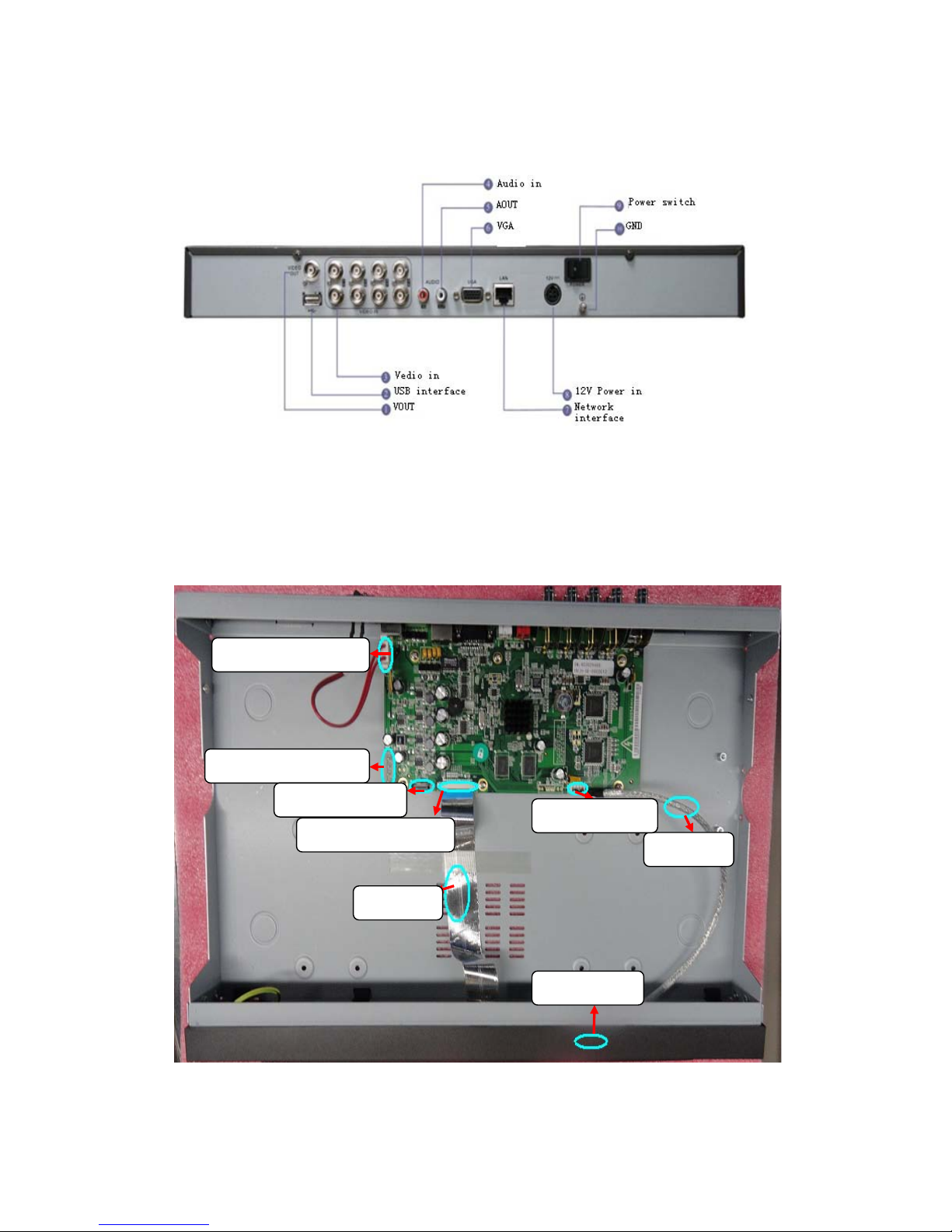
1. DS7208HVI-ST/SE Equipment Physical Interface
Note: DS7208HVI-ST/SE equipment some no RS485 interface
2. DS7208HVI-ST/SE Equipment Internal Structure
SATA power interface
Front-panel
12V power interfac
SATA interface
Panel line interface
Panel line
USB line
USB interface
Page 4
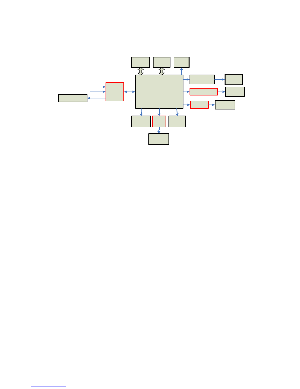
3. DS80054 Mainboard Hardware Principle Diagram
DSP
Network
(RTL8201)
TW2866
(US1)
FLASHDDR∏
SP491
SGM9111
UTP
Interface
USB
VGA
Interface
VOUT
Interface
SATA
interface
LVC07A+6303
RS232
interface
RS485
interface
Audio in
Video in
Audio out
AOUTinterface
Diagram1.1 DS80054 Hardware P rinciple Diagram
Note:
TW2866 (US1) support 1 r oad audio and 4 roa d video input, voice talkback Line In input
and AOUT output
VGA signal output directly from KY2010 chip, the external circ uit by LVC07A + 6303
control VGA outpu t a m p lification
VOUT signal directly from KY2010 chip output, th e external circu it c ontrol by SGM 911 1
VOUT signal amplifier output
no alarm input/ou t of modules
Page 5
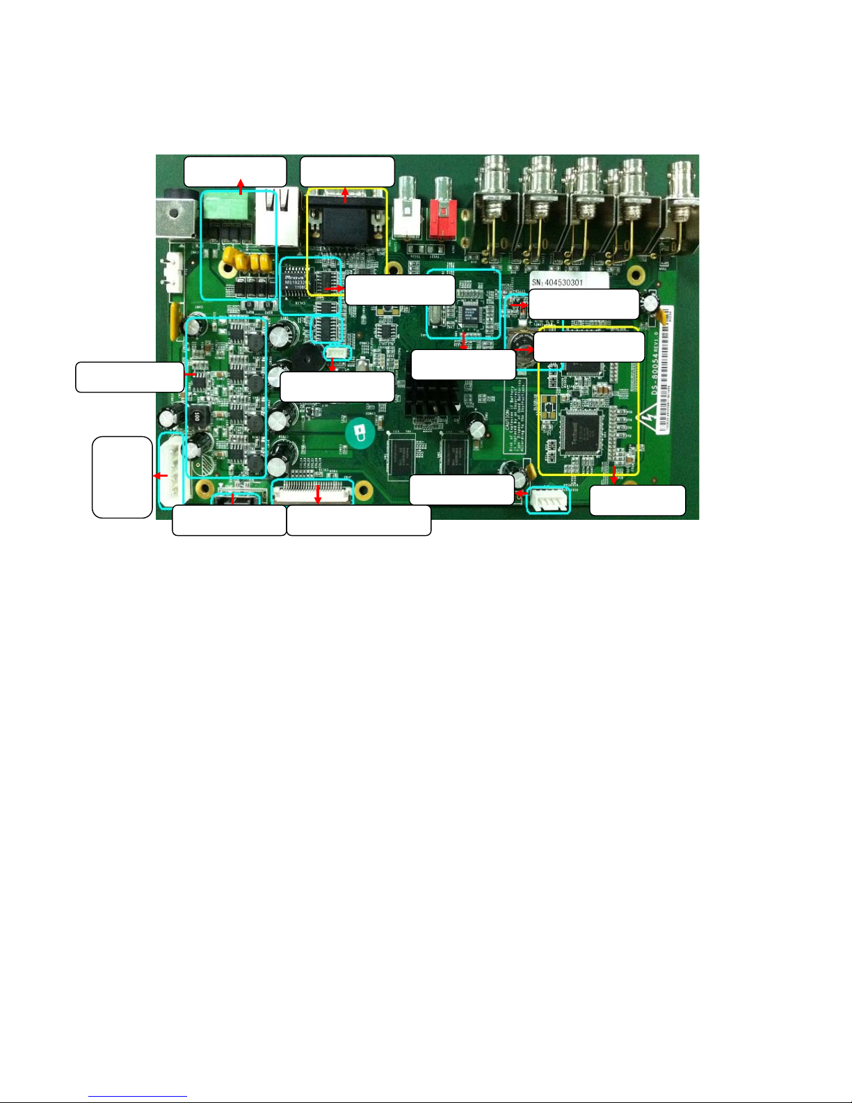
4. DS80054 Mainboard Hardware Modules Diagram
Diagram 1.2 DS80054 Mainboard Hardware Modules Diagram
5. DS80054 Mainboard Hardware Module Introduction
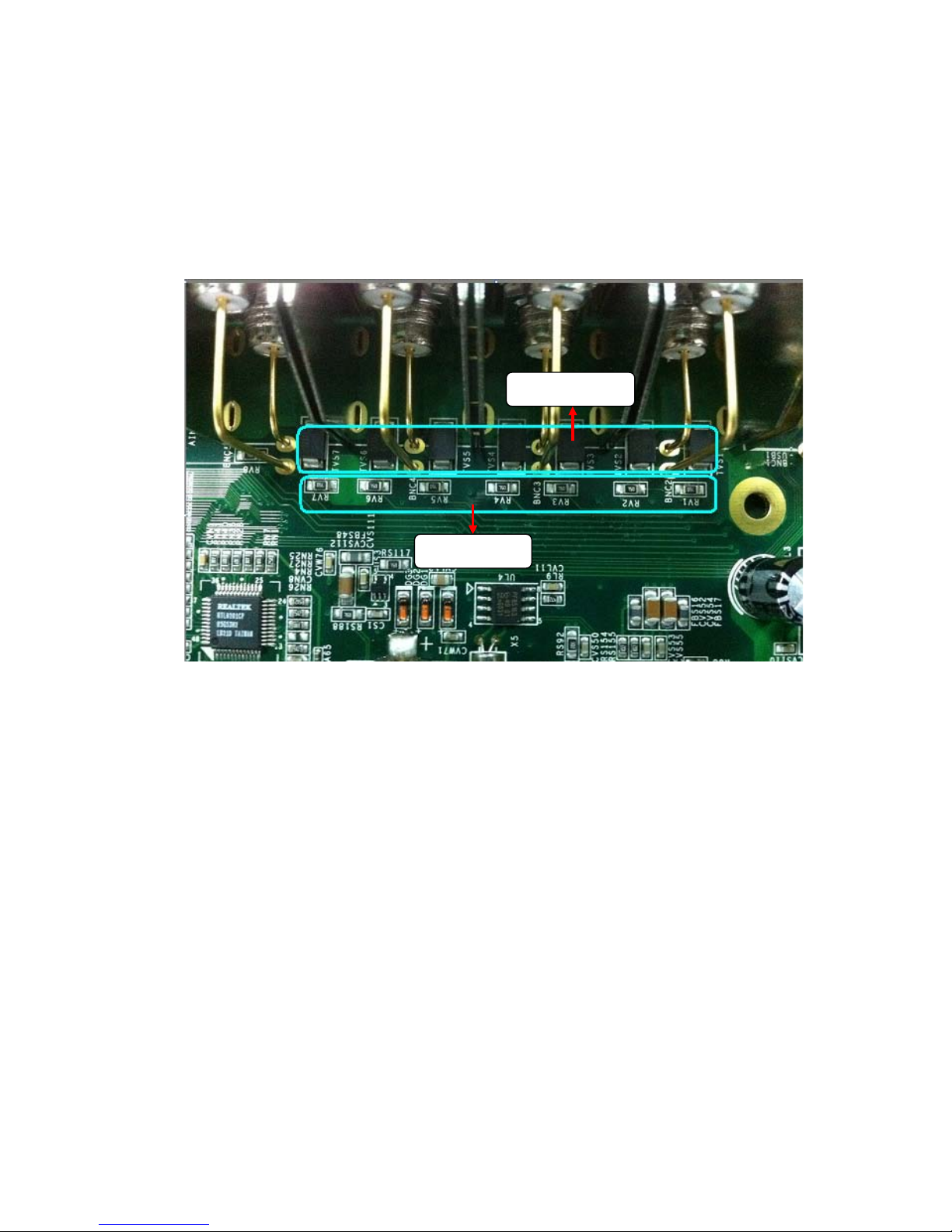
5.1. Audio Vide o A/D Module
Video A/D Module Main Control Chip:TW2866 Audio
1) TW2866(US1)P IN 6 control fi rst audio input (input matching re sistance
100 (RU9) and capacitance (CS18))
2) TW2866(US1)PIN 13/1 7/21/25 control 1-4 road vedio input (BNC i nput
matching 4 HK-5 production tube( TVS2/4/6/8); 4 75Ωresistance
( RV2/4/6/8 ); 4 100Ωresistance ( RU1/2/3/4 ); 4 capacitance
(CS12/8/13/11))
3) TW2866(US2)PIN 13 /17/21/25 control 5-8 road vedio input (BNC i nput
matching 4 HK-5 production tube( TVS1/3/5/7); 4 75Ωresistance
VGAmodule
RS485module
USB interface
Network module
VOUT module
SATA
power
module
A/D module
Power module
SATA interface
Clock module
RS232 interface
Network module
Front-panel interface
Page 6
( RV1/3/5/7 ); 4 100Ωresistance ( RU5/6/7/8 ); 4 capacitance
(CS42/48/29/33))
27 M (Y4) : TW2866 work clock, PIN 82 input 27 M
Audio video A/D module component:
75Ω(RV1-8)
HK-5(TVS1-8)
Page 7

5.2. VGA Output Module (Local Preview Image Output Mo dule)
VGA main chip module: LVC07A, 6303; LVC 07A PI N 2 o utp ut si ngle(V S)
and 1 K resi stance (RL 50) conne ct 5V vol tage, PIN 4 output si gnal (HS) and
1 K (RL51) resistance co n nect 5V voltage
BAV99: control VGA output amplification, if BAV99 (Q9) 3 feet low level
(voltage 0 V), it mea ns the sys tem to de tect V GA display ; If you me et VGA
display, system and output si gnal and syste m menu VGA; If be hind the VGA
display, the syste m only output VGA signal; If the high level (close to 3.3 V),
it means the system does not detect the display
VGA signal output basic schemes:
27M(X4)
100Ω(RU1-4)
(
CS12/8/13/11)
100Ω(RU9)
TW2866(US1)
(
CS18)
100Ω(RU5-8)
(
CS42/48/29/33)
TW2866(US2)
Page 8

① : PIN 10 output “R” signal ;
② : PIN 1 1 output “B” signal ;
③ : PIN 12 output “G” signal ;
④ : PIN 4 output “HS” signal ;
⑤ : PIN 2 output “VS” signal ;
VGA master chip : 74LV07 and 6303
Description:
74LV07
PIN4
PIN2
5V
5V
RL50
1K
Ω
RL51
1K
Ω
VS(Interlacing signal)
HS(Line signal)
BAV99 :
If the PIN 3 of BAV99(Q9) is Low-level ( 0V ), Said system detects VGA
monitor;
If the PIN 3 of BA V99(Q 9) is high-leve l (nearly 3.3V), said syste m doesn’t detect
VGA monitor;
VGA module components:
6303
74LV07
75Ω(RG6)
75Ω(RG5)
75Ω(RG4)
BAV99(Q3)
BAV99(Q8)
BAV99(Q7)
②
①
③
④
⑤
Page 9

5.3 .VOUT Output Module (Local Preview Image Output Module)
VOUT main control chip: SGM9111, PIN 3 pull-down 75Ωresistance
(RS188) groundi ng and in pu t CVBS -OUT signal, PIN 4 through the
75Ωresistanc e (RS117) output VOUT signal, working voltage through a
WCX(FBS48) for 5V power supply
VOUT interface TVS protection tube: VOUT interface connect HK-5 (TVS9)
VOUT signal output basic schemes:
LVC07A
BAV 99(Q3/7/8/9)
6303
75Ω(RG4/5/6)
1K(RL50/51)
33Ω(RG30/31)
Page 10

SGM9111
CVBS-VOUT
Pin3 input
75Ω
(RS188)
Pin4 output
75Ω(RS117)
VOUT
FBS48
5V
DSP
Pin5
VOUT Module components:
5.4. Network Module
Network module components:
SGM9111
75Ω(RS117)
WCX(FBS48)
75Ω(RS188)
HK-5(TVS9)
Page 11

5.4.1 LAN master chip :
Chip name pin Description voltage
RTL8201 36
Operation voltage
input “pin 36” via
“FBN1”
V≈3.3V
5.4.2 Transformer
Chip name Description
MS10232NL
Network transmission sig nal
amplification, rectificat ion
5.4.3 Crystal
Chip name Description
25M(Y3) RTL8201 clock chip
5.4.4 Signal amplification chip :
U2.8(UN3) : used to amply signal transmission (TX) / Receiv e ( RX ) ;
5.5. SATA Module
SATA main control chip: KY2010
BD9329(U2) power piece: PIN 2 enter 12 V, PIN3 output 5V for SATA power
source
SATA module part:
U2.8
MS10232
RTL8201
25M(Y3)
WCX(FBN1)
Page 12

5.6. RS485 Module
RS485 main control chip: SP491EEN, PIN 9, 10 were TX +,TX-,the
difference voltage close to 5 V
TVS: B03NC (BA5/6/7/ 8), HK-4 (D2/3 /4/ 5) pr otect the se ndi ng end (TX +,
TX-R +, R-)
Thermistors (JK250) : JK250 (RPT1/2/3/4) protect the sending end (TX +,
TX-R +, R-)
RS485 module part:
SATA interface
SATA
power
interface
B03NC(BA5/6/7/8)
SP491EEN
JK250(RPT1/2/3/4)
HK-4(D2/3/4/5)
BD9329(U2)
Page 13

5.7. Clock Module
Clock control chip: 8563 T
32768 HZ: 8563 T reset the clock
Battery: External Battery, normal voltage 3.3 V
Diodes (DG1, DG2, DG3) : DG1 co nne cts to 3 .3 V vol ta ge, DG 2, DG3
Battery are co nnected at one end , when the mainbo ar d el ectricity, DG2,
DG3 globe, DG1 conduction, Battery don't power supply; When the
mainboard power cuts, in turn, the Battery power supply, DG2, DG3
conduction, DG1 deadline
The clock module component
8563T
UL4
1
2
3
4
8
7
6
5
DG1
BATTERY
3.3V
DG2
DG3
3.3V
X1
32768Hz
8563T
32768HZ
Battery
Diode
Page 14

5.8. Voice Talk back Module
Voice talkback module main control chip: TW2866 (US1), PIN 2 through
3.9 K resistance (RS60) + 560Ωresistance (RP24) output Aout
Voice talkback module pa rt:
(note: voice talkback Line In input and the first road audio input share)
5.9. Power Supply Module
The power module component:
560Ω(RP24)
TW2866(US1)
3.9K(RS60)
Page 15

BD9328 (U1) : PIN 2 enter 12 V, PIN 3 output 5 V, mainly used for other
components provide normal work voltage
BD9329 (U2) : PI N 2 enter 1 2 V,PIN 3 output 5 V , mainly fo r the SAT A hard
disk normal powe r BD9328 (U3) : PI N 2 enter 12 V,PIN 3 3.3 V, mainl y used
for other components provide normal working voltage, power of MP8904
turn 1.2 V output
BD9328 (U4) : PIN 2 enter 12 V,PIN 1 output 1.8 V, mainly for the KY2010
system working voltage and DDR2 memory work voltage
BD9328 (U5) : PI N 2 ente r 12 V,PI N 1 o utp ut 1.0 V , m ainly fo r t he K Y2010
system start working voltage
MP8904 (UV3) :PI N 8 input 3.3 V,PIN 1 output 1.2 V, mainly for the TW2866
chip normal working voltage
BD9329(U2)
BD9328(U3)
BD9328(U1)
BD9328(U4)
BD9328(U5)
Page 16

6. DS80054 Mainboard Failure Analysis
VGA and VOUT and output image, but not at the same time output system
menu, the system default first detection VGA output, then detection VOUT
output
6.1. First Meet VGA Display
Boot to meet VGA monitor (or also meet VGA display and VOUT monitor),
BAV99 (Q9) PIN 3 low level effective, display output VGA signal and system
menu, monitor only VOUT signal
6.2. First Meet VOUT Monitor
Boot first meet VOUT monitors, BAV99 (Q9) 3 feet is high level, the high level
signal feedback to the CPU, monitor output VOUT signal and system menu,
display show only the VGA signal
Note: ① BAV99 (Q9) 3 feet high le vel, only o utput signal VG A monitor, monitor
and output signal and system VOUT menu
② BAV99 (Q9) 3 feet low level, di splay and VGA output signal and system
menu, monitor only output VOUT signal
6.3 Fault Analysis
①. No VGA Output
Step 1: measure 1 K resist ance (RL50/5 1), or replace ment (1 K val ue too large,
LVC07A chip PIN 2 VS signal output, PIN4 HS signal output voltage
value will be lower, then cause no VGA output)
Step 2: measurement 33Ωresistance (RG30/31), or replacement
Step 3: using a multimeter to measure LVC07A PIN 1 input (VS signal) voltage
about 3.3V and PI N 3 i np ut ( HS sig nal) voltage 3V also, and then
measure PIN 2 ou tp ut (V S signal) voltage about 5V, the PIN4 o ut pu t
(HS signal) voltage about 4.3V, otherwise LVC07A ruled out
Step 4: measuremen t cap aci ta nce CG1, CG2 impedance , or repl ace me t
Page 17

②. No VOUT Output
Step 1: measurement HK-5 (TVS9) whether short circuit, or replacement
Step 2: measuring 75Ωresistance (RS117) impedence, or replacement
Step 3: monitor’s signal lines connected to the probe, directly from SGM9111
(US7) chip PIN 4 draw out the VOUT signal, or replacement
Step 4: measuring 75Ω resistance (RS188), or re placement, and then monitor’s
signal lines connected to the probe, directl y lead CVBS -VOUT signal
from 75Ω resistance (RS188) end, or KY2010 ruled out
③. Image Problem
Phenomenon 1 : there is no video si g nal , fi r st e xcl u de HK -5 (TVS1-8) whether
short circuit, or replac e men t; Me as u rin g 75Ω(RV1-8) resistance, or
replacement, and then ruled out 100Ωresistance (RU1-8); Finally ruled out
TW2866 (can directly introduce video signal into TW2866 chip video input
end,PIN13/17/21/25, to rule out the chip is normal or not)
Phenomenon 2 : a fe w cha nnel image blac k sc re e n, f ir st r u le ou t the so ftw are
settings, o therwise int roduce video signal into TW28 66 chip video i nput end,PIN
13/ 17/21/25, to rule out the chip is normal , or repla ce me nt
Phenomenon 3: all black and white images or flower screen, to rule out 27 M
(Y4), then rule out software, or change TW2866
CG1,CG2
Page 18

④. Voice Problems
Phenomenon 1: preview no voi ce , fi rs t w it hout software Se tti n g s, t he n
measuring 100 resistance (RU9) and capacitance (CS18) impedance, or
replacement, finally ruled out TW2866 (US1) (can directly introduce audio
signal into TW2866 chi p audio input PIN 6, to rule ou t the chip is normal o r not)
Phenomenon 2: voice talkback AOUT no output, measuring 3.9 K resistance
(RS60) + 560 Europe resistance (RP24) resistance , or replacement, finally ruled
out TW2866 (US1) (directly lead AOUT signal from the TW2866 chip PIN2, to
exclude the chip is normal or not)
⑤.RS485 Failure
Step 1: the first to exclude thermistors JK250 (RPT1/2/3/4)
Step 2: measurement TVS tube B 03 NC (BA 5/ 6/7/ 8 ), HK-4 (D2/3/4/5)
impedance, or replacement
Step 3: measurement SP491E EN 9 and 10 feet chip diffe rence vol tage (no rmal
close to 5 V), or replacement
⑥. Internet Links
Network light and network data transmission light are flashing
Step 1: first mea surement RTL820 1 chip PIN 36 inp ut voltage 3.3V i s normal, or
to measure WCX (FBN1) impedance, or replaceme n t
Both network light and network data transmission light not bright
Step one: first measurement 25 M (Y3) crystal, or replacement
Step two: replace RTL8201
Both network light and network data transmission light are nomal
Step one: first replace RTL82 01, an d the n rule d out MS1 02 32, U2.8
⑦.SATA Hard Dish Fault
Step one: first measurement BD9329(U2) PIN 3 power output voltage wheather 5V or short
circuit, or replacement
Page 19

⑧. Clock Fault
Step one: the first to rule o ut the battery (normal volta ge 3.3 V), an d then ruled
out 8563 T, 32768 HZ, diodes
⑨.VGA Output Color Devation
Step 1: measuring 75Ω resistance (RG4/5/6), or replacement
Step 2: measurement BAV99 (Q3/ 7/8) PIN 3 impenda nce to GN D, or
replacement
Step 3: rule out 6303 chip
⑩.USB Fault
Step one: measurement SESR05 (QA1 or QA2) 2, 3 feet voltage difference
value (normal voltage diff erence about 3.05 V), as well as the impedance to the
GND, or replacement
Note: SESR05 (QA1 or QA2),front and after USB interface is independent of
each other
SESR05(QA2)
SESR05(QA1)
Page 20

Schedule: 1 Crystal Effect
Schedule:2 Voltage Effect
Serial
number
Crystals Action (devices work clock )
1
27M(Y4)
TW2866 chips work clock (82 fee t input 27 M)
2
25M(Y3)
RTL8201 chips work cl ock
3
24M(Y1)
KY2010 system startup
clock, and integrated USB
module clock
The serial
number
Power chip function (devices working voltage)
1
BD9328(U1)
2 feet enter 12 V, 3 feet output 5 V, mainly used for
other components provide normal work voltage
BD9328(U5)
2 feet enter 12 V, foot 1 output 1.0 V, mainly for the
KY2010 system start working voltage
BD9328(U3)
2 feet enter 12 V, 3 feet 3.3 V, m ainly used f o r o the r
components provide normal working voltage, power
of MP8904 turn 1.2 V output
BD9328(U4)
2 feet enter 12 V, foot 1 output 1.8 V, mainly for the
KY2010 system worki n g vol ta ge an d DDR2 memory
work voltage
2
BD9329(U2)
2 feet enter 12 V, 3 feet output 5 V, mainly for the
SATA hard disk normal power
3 MP8904
(UV3)
feet 8 input 3.3 V, foot 1 output 1.2 V, mainly for the
TW2866 chip normal worki n g vol ta ge
 Loading...