


HF-Z100 ZigBee Module User Manual
HF-Z100
LIST OF FIGURES
LIST OF TABLES
HISTORY
1. PRODUCT OVE RVIEW
1.1. General Description
1.2. Device Features
1.3. Device Paremeters
1.4. Key Application
.................................................................................................................................................................
.................................................................................................................................................
...................................................................................................................................................
......................................................................................................................................
.................................................................................................................................
.......................................................................................................................................
ZigBee Module User Manual
V1.2
TABLE OF CONTENTS
............................................................................................................................
...............................................................................................................................
2
2
2
3
3
3
4
4
2. HARDWARE INTRODUCTION
2.1. Pins Definition
2.2. Electrical Characteristics
2.3. Mechanical Size
2.4. Antenna
2.5. Evaluation Kit
2.6. Order Information
2.7. Typical Application
3. PACKAGE INFORMATION
3.1. Recommended Reflow Profile
3.2. Device Handling Instruction (Module IC SMT Preparation)
3.3. Shipping Information
APPENDIX A: HW REFERE NCE DESIG N
APPENDI X B: CONTACT INFO RMA TIO N
.........................................................................................................................................
......................................................................................................................................
....................................................................................................................................................
..........................................................................................................................................
.................................................................................................................................
...............................................................................................................................
............................................................................................................................
..............................................................................................................
.......................................................................................................................
...................................................................................................................
............................................................................................................
...............................................................................................
................................................................................................
..........................................................
5
5
6
6
7
9
10
10
11
11
11
11
13
14
Shanghai High-Flying Electronics Technology Co., Ltd(www.hi-flying.com) -1-

HF-Z100 ZigBee Module User Manual
LIST OF FIGURES
Figure 1. HF-Z100 Overview
Figure 2. HF-Z100 Pins Map
Figure 3. HF-Z100 Mechanical Dimension
Figure 4. HF-Z100 Suggested Wire Antenna Position
Figure 5. HF-Z100 through hole PAD Position
Figure 6. HF-Z100 with Chip Antenna Suggested Placement
Figure 7. HF-Z100 Evaluation Kit
Figure 8. HF-Z100 Order Information
Figure 9. HF-Z100 Hardware Typical Application
Figure 10. Reflow Soldering Profile
Figure 11. Shipping Information
.............................................................................................................................
.............................................................................................................................
......................................................................................................
..................................................................................
...............................................................................................
.....................................................................................................................
............................................................................................................
........................................................................................
..............................................................................................................
....................................................................................................................
LIST OF TABLES
Table 1. HF-Z100 Module Technical Specifications
Table 2. HF-Z100 Pins Definition
Table 3. Operation Parameters
Table 4. RF Parameters
Table 5 HF-Z100 Evaluation Kit Interface Description
Table 6. Reflow Soldering Parameter
.......................................................................................................................................
........................................................................................................................
...........................................................................................................................
..............................................................................................................
........................................................................................
...................................................................................
.....................................................................
5
5
7
8
8
8
9
10
10
11
12
4
5
6
6
9
11
HISTORY
Ed.V1.0 04-10-2014 First Version.
Ed.V1.1 05-18-2014 Update Antenna Option and add EVK information.
Shanghai High-Flying Electronics Technology Co., Ltd(www.hi-flying.com) -2-

HF-Z100 ZigBee Module User Manual
1. PRODUCT OVERVIEW
1.1. General Description
The HF-Z100 is a fully self-contained, small form-factor, IEEE802.15.4 Zigbee modulewith low
complexity, self-organizing, lowpower, low cost feature.It is based on IEEE802.15.4 standard, can be
coordinated toachieve communication between the thousands of tiny sensors that require very
littleenergy to relay the data through radio waves from one sensor to another sensor, thus withhigh
communication efficiency.
The HF-Z100 employs the world's lowest power consumption embedded architecture. It has been
optimized for all kinds of Zigbee applications in the home automation, smart grid, smart lighting,
handheld device, personal medical application and industrial control that have lower data rates, and
transmit or receive data on an infrequent basis.
The HF-Z100 integrates all IEEE802.15.4 Zigbee functionality into a low-profile,15.6x12.2x2.0mmSMT
module package that can be easily mounted on main PCB with application specific circuits. Also,
module provides built-in antenna, external antenna option.
1.2. Device Features
Size: 15.6x12.2x2.0mm Smallest size module;
High RX sensitivity:≤-101dBm;
Excellent link budget: > 110dB;
Max output power: 9dBM +/- 1.5dBm;
Extend OperationTemprture: -40℃-110℃for smart lighting application;
Low power consumption:
Operating Current: < 150mA
Deep Sleep Current: <10uA
512KB Internal Flash, 160KB SRAM resource for customized application;
Full Zigbee ZHA/ZLL profile supported;
Various peripherals interface:
15 x GPIO ports
3 x 16-bit ADC input channel
2 x UART with hardware flow control
1 x SPI interface
1 x I2C interface
SWD debug interface
Power Supply Range from 2V to 3.6V, support battery supply application;
High performance on-board antenna and PAD/HOLE for external antenna option;
CE/FCC/RoHS certification;
Shanghai High-Flying Electronics Technology Co., Ltd(www.hi-flying.com) -3-
HF-Z100 ZigBee Module User Manual
1.3. Device Paremeters
Table 1. HF-Z100 Module Technical Specifications
Class Item Parameters
Certification FCC/CE
Wireless Standard 802.15.4
Radio Data Rate
Wireless
Parameters
Hardware
Parameters
Frequency Range
Transmit Power 9 +/-1.5dBm
ReceiverSensitivity
Antenna Option
Data Interface
Operating Voltage 2.0~3.6V
Operating Current
Deep Sleep Current
Communication
Distance
Operating Temp.
StorageTemp.
Dimensions and Size 15.6x12.2x2.0mm
250Kbps@2.4GHz
2.4~2.4835GHz
≤-101dBm
External:
PAD or Through Hole for external ANT
Internal:On-board Chip ANT
UART,ADC,DAC
SPI,I2C,GPIO
80mA
<
10uA
<
Indoor 30m,Outdoor 100m
-40℃-110
-45℃-125
℃
℃
1.4. Key Application
Illumination control
HVAC monitoring and control
Building automation
Access Control
Security system
Industrial automation
Automated metering
Smart energy
Shanghai High-Flying Electronics Technology Co., Ltd(www.hi-flying.com) -4-
HF-Z100 ZigBee Module User Manual
2. HARDWARE INTRODUCTION
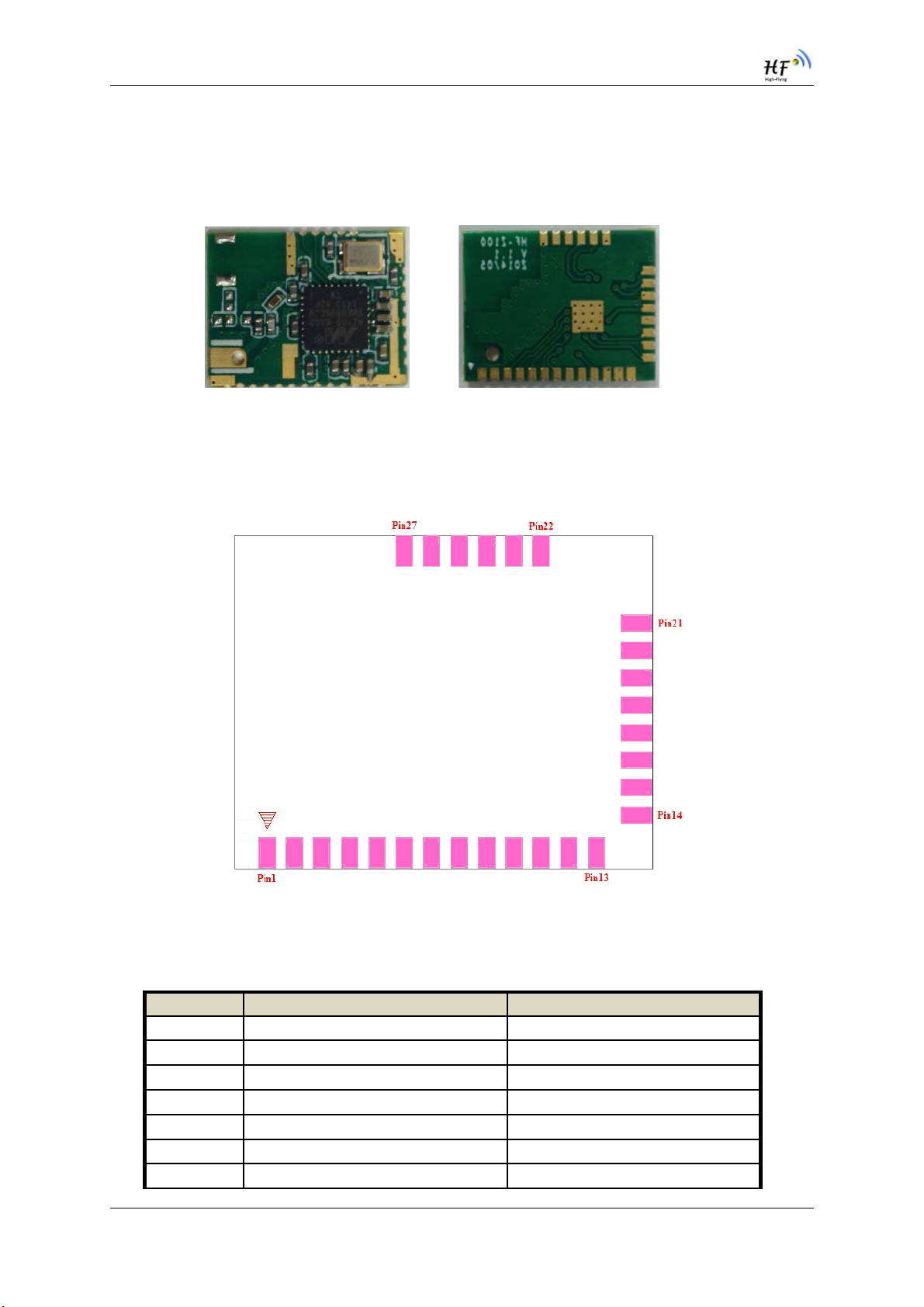
Figure 1. HF-Z100 Overview
2.1. Pins Definition
Figure 2. HF-Z100 Pins Map
Table 2. HF-Z100 Pins Definition
Pin Net Name Describtion
1~2 GND Ground
3 GPIO12 PWM output-1 (Timerl)
4 GPIO13 PWM output-2 (Timerl)
5GPIO14 SWDClock
6 GPIO15 SWD Data
7 GPIO16 IIC SDA
8VIO IO Power (2.0~3.6V)
Shanghai High-Flying Electronics Technology Co., Ltd(www.hi-flying.com) -5-

HF-Z100 ZigBee Module User Manual
Pin Net Name Describtion
9GPIO17 IICCLK
10 GPIO18 PWM output-3 (Timerl)
11~13 GND Ground
14 GPIO21 UART2_TXD
15 GPIO22 UART2_RXD
16 GPIO23 PWM output-4 (Timerl)
17 GND Ground
18 VBAT Main Power (2.0~3.6V)
19 GND Ground
20 GPIO29 Reserve
21 GPIO28 Enable
22 GND Ground
23 RESET_N The reset signal
24 GPIO4 ADCx3 or ADCx1
25 GPIO5
26 GPIO6
27 GND Ground
And Wakeup INTx2
2.2. Electrical Characteristics
Table 3. Operation Parameters
Parameter Condition Min. Typ. Max. Unit
Operating Supply voltage 2.0 3.3 3.6 V
RX Current Active CPU 32MHz 21 mA
TX Current Active CPU 32MHz, +9dBm 34 mA
Deep Sleep Current 10 uA
Table 4. RF Parameters
Parameter Ratings Unit
Operating Frequency
IF Frequency 4 MHz
Quantity of Channel 16
Number of Channeels 11~26
Max TX Power 9 dBm
RX Seneitivity ~104 dBM
Data Rate 250 KBS
2.4~2.4835
GHz
2.3. Mechanical Size
HF-Z100 modules detailed mechanical data is referred to as following Figure(Unit is Mil).
The pad size:25mil X 45mil, pin pitch is 40mil.
Shanghai High-Flying Electronics Technology Co., Ltd(www.hi-flying.com) -6-

HF-Z100 ZigBee Module User Manual
Figure 3. HF-Z100 Mechanical Dimension
2.4. Antenna
HF-Z100 module support internal on-board chip antenna and external wire antenna
option.Wire antenna is flexible to avoid the metal affect or the other on RF performance in
LED lighting because it isnot fixed on board like chip antenna and can be go out externally.
The position for the assembly of wireantenna on board referto Figure 4, user can select
horizontal direction through the SMT PAD or vertical direction through the Through Hole PAD
based on dedicated application.
When customer select internal antenna, you shall comply with following antenna design rules
and module location suggestions:
For user PCB, RED color region (6x5mm) can’t put componet or paste GND net;
Antenna must away from metal or high components at least 10mm;
Antenna can’t be shieldedby any meal enclosure. All cover, include plastic, shall away
from antenna at least 10mm;
High-Flying suggest HF-Z100 module better locate in following region at customer board as
Figure 5, which to reduce the effect to antenna and wireless signal, and better consult HighFlying technical people when you structure your module placement and PCB layout.
Shanghai High-Flying Electronics Technology Co., Ltd(www.hi-flying.com) -7-

HF-Z100 ZigBee Module User Manual
Figure 4. HF-Z100 Suggested Wire Antenna Position
Figure 5. HF-Z100 through hole PAD Position
The through hole PAD Position:
X: 95mil
;Y:91.5mil;Dia.:35.43mil
Figure 6. HF-Z100 with Chip Antenna Suggested Placement
Shanghai High-Flying Electronics Technology Co., Ltd(www.hi-flying.com) -8-

HF-Z100 ZigBee Module User Manual
2.5. Evaluation Kit
High-Flying provides the evaluation kit to promote user to familiar the product and develop the detailed
application. The evaluation kit shown as below, user can connect to HF-Z100 module with the UART
(USB), or SWD Debugger port to configure the parameters, manage the module or do the some
functional tests.
Figure 7. HF-Z100 Evaluation Kit
Notes:
The external interface description for evaluation kit as follows:
User need consult high-flying for software SDK support or more detailed debug support.
Table 5 HF-Z100 Evaluation Kit Interface Description
Function
External
Interface
LED
Button
Name Description
JTAG JTAG data debug interface (Not for user use)
USB
DC Jack
DC5-9V DC jack for power in, 5~9V input.
BAT
EXT PORT HF-Z100 GPIO function extend interface connector
Power 3.3V Power Indicator
TXD UART TXD Indicator
RXD UART TXD Indicator
nReset Used to reset the module.
UART to USB debug interface. (For PC without
RS232, need load driver). Can be Power input.
DC jack for power in, 5~9V input.
2 Li-Battery Power Supply.
Shanghai High-Flying Electronics Technology Co., Ltd(www.hi-flying.com) -9-

HF-Z100 ZigBee Module User Manual
2.6. Order Information
Base on customer detailed requirement, HF-Z100 series modules provide different variants and
physical type for detailed application.
Figure 8. HF-Z100 Order Information
2.7. Typical Application
The module basic reference schematic is referred to following,
Figure 9. HF-Z100 Hardware Typical Application
Notes:
suggestusing them as the default UART download port.
Shanghai High-Flying Electronics Technology Co., Ltd(www.hi-flying.com) -10-
If HF-Z100 GPIO6 (RXD) and GPIO4 (TXD) are not used for ADC and Wakeup function,

HF-Z100 ZigBee Module User Manual
3. PACKAGE INFORMATION
3.1. Recommended Reflow Profile
Figure 10. Reflow Soldering Profile
Table 6. Reflow Soldering Parameter
NO. Item Temperature (Degree)
1 Reflow Time Time of above 220 35~55 sec
2 Peak-Temp 260 max
Note:
1. Recommend to supply N2 for reflow oven.
2. N2 atmosphere during reflow (O2<300ppm)
Time(Sec)
3.2. Device Handling Instruction (Module IC SMT Preparation)
1. Shelf life in sealed bag: 12 months, at <30℃and <60% relative humidity (RH)
2. After bag is opened, devices that will be re-baked required after last baked with window time
168 hours.
3. Recommend to oven bake with N2 supplied
4. Recommend end to reflow oven with N2 supplied
5. Baked required with 24 hours at 125+-5℃before rework process for two modules, one is
new module and two is board with module
6. Recommend to store at≦10% RH with vacuum packing
7. If SMT process needs twice reflow:
(1) Top side SMT and reflow (2) Bottom side SMT and reflow
Case 1: Wifi module mounted on top side. Need to bake when bottom side process over 168
hours window time, no need to bake within 168 hours
Case 2: Wifi module mounted on bottom side, follow normal bake rule before process
Note:
Window time means from last bake end to next reflow start that has 168 hours space.
3.3. Shipping Information
Shanghai High-Flying Electronics Technology Co., Ltd(www.hi-flying.com) -11-

HF-Z100 ZigBee Module User Manual
TAPE BOX
Size: 340*340*70 mm Size: 340*340*350 mm (inside)
Figure 11. Shipping Information
To Be Update
Note:
1 tape = 500pcs
1 box = 5 tapes = 5 * 500 pcs = 2500pcs
Shanghai High-Flying Electronics Technology Co., Ltd(www.hi-flying.com) -12-

HF-Z100 ZigBee Module User Manual
APPENDIX A: HW REFERENCE DESIGN
Detailed HF-Z100 Evluation Board design source files, pls access High-Flying web download page or
contact with High-Flying technical support people to acquire.
Shanghai High-Flying Electronics Technology Co., Ltd(www.hi-flying.com) -13-

HF-Z100 ZigBee Module User Manual
APPENDIX B: CONTACT INFORMATION
-----------------------------------------------------------------------------------------------------------Address: Room.511/510, Building 7, No.365, Chuanhong Road,Pudong New Area,
Shanghai, China, 201202
Web:www.hi-flying.com
Service Online: 400-189-3108
Sales Contact: sales@hi-flying.com
-----------------------------------------------------------------------------------------------------------
For more information about High-Flying modules, applications, and solutions, please visit our web site
http://www.hi-flying.com/en/
<END OF DOCUMENT>
© Copyright High-Flying, May, 2011
The information disclosed herein is proprietary to High-Flying and is not to be used by or disclosed to
unauthorized persons without the written consent of High-Flying. The recipient of this document shall respect the
security status of the information.
The master of this document is stored on an electronic database and is “write-protected” and may be altered only
by authorized persons at High-Flying. Viewing of the master document electronically on electronic database
ensures access to the current issue. Any other copies must be regarded as uncontrolled copies.
Shanghai High-Flying Electronics Technology Co., Ltd(www.hi-flying.com) -14-

FCC INFORMATION (USA) FCC STATEMENT
1. This device complies with Part 15 of the FCC Rules. Operation is subject to the
following two conditions:
(1) This device may not cause harmful interference.
(2) This device must accept any interference received, including interference that may
cause undesired operation.
CAUTION: Changes or modifications not expressly approved by the party responsible for
compliance could void the user's authority to operate the equipment.
NOTE: This equipment has been tested and found to comply with the limits for a Class B
digital device, pursuant to Part 15 of the FCC Rules. These limits are designed to provide
reasonable protection against harmful interference in a residential installation. This
equipment generates uses and can radiate radio frequency energy and, if not installed
and used in accordance with the instructions, may cause harmful interference to radio
communications. However, there is no guarantee that interference will not occur in a
particular installation. If this equipment does cause harmful interference to radio or
television reception, which can be determined by turning the equipment off and on, the
user is encouraged to try to correct theinterference by one or more of the following
measures:
- Reorient or relocate the receiving antenna.
- Increase the separation between the equipment and receiver.
- Connect the equipment into an outlet on a circuit different from that to which the
receiver is connected.
- Consult the dealer or an experienced radio/TV technician for help.
FCC Radiation Exposure Statement:
This equipment complies with FCC radiation exposure limits set forth for an uncontrolled
environment. This equipment should be installed and operated with minimum distance
20cm between the radiator & your body.
OEM INTEGRATION INSTRUCTIONS:
This device is intended only for OEM integrators under the following conditions:The
module must be installed in the host equipment such that 20 cm is maintained between
the antenna and users, and the transmitter module may not be co-located with any other
transmitter or antenna. The module shall be only used with the internal on-board antenna
that has been originally tested and certified with this module. External antennas are not
supported.
As long as these 3 conditions above are met, further transmitter test will not be required.
However, the OEM integrator is still responsible for testing their end-product for any
additional compliance requirements required with this module installed (for example,

digital device emissions, PC peripheral requirements, etc.). The end-product may need
Verification testing, Declaration of Conformity testing, a Permissive Class II Change or
new Certification. Please involve a FCC certification specialist in order to determine what
will be exactly applicable for the end-product.
Validity of using the module certification:
In the event that these conditions cannot be met (for example certain laptop
configurations or co-location with another transmitter), then the FCC authorization for this
module in combination with the host equipment is no longer considered valid and the
FCC ID of the module cannot be used on the final product. In these circumstances, the
OEM integrator will be responsible for re-evaluating the end product (including the
transmitter) and obtaining a separate FCC authorization. In such cases, please involve a
FCC certification specialist in order to determine if a Permissive Class II Change or new
Certification is required.
Upgrade Firmware:
The software provided for firmware upgrade will not be capable to affect any RF
parameters as certified for the FCC for this module, in order to prevent compliance
issues.
End product labeling:
This transmitter module is authorized only for use in device where the antenna may be
installed such that 20 cm may be maintained between the antenna and users. The final
end product must be labeled in a visible area with the following: “Contains FCC ID:
2ACSV-HF-Z100”.
Information that must be placed in the end user manual:
The OEM integrator has to be aware not to provide information to the end user regarding
how to install or remove this RF module in the user's manual of the end product which
integrates this module. The end user manual shall include all required regulatory
information/warning as show in this manual.
 Loading...