

Page 1
User Manual
HBR-DS-19001 - March 2019 (version 1.1)
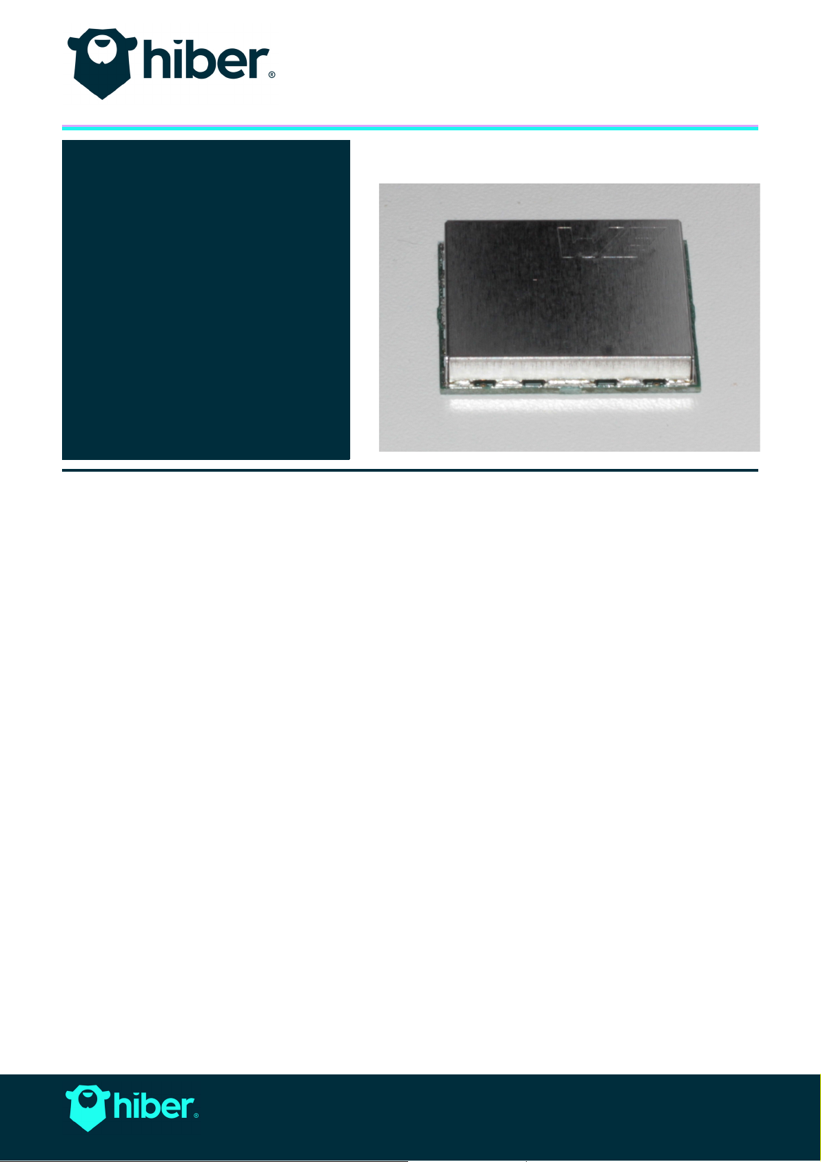
Key features
Hiberband modem
• Compact, ultra low-power SMT
module design
• Hiberband RF signal and
baseband processing
• Interface for direct connection of
a GNSS receiver module
• Geolocation-based satellite
tracking algorithm
• Serial UART-based host
processor interface
Functional description
The Hiberband modem is a highly integrated, low-power communications front-end designed for global delivery
of sensor data through Hiber’s satellite-based Hiberband Low-Power Global Area Network (LPGAN). Designed as
a compact, solderable SMT module, it is straightforward to integrate in IoT devices. The application host processor
of the IoT device interacts with the Hiberband modem through a UART-based serial interface using a commandresponse protocol.
The Hiberband modem operates in one of several modes, each with their own distinctive power consumption
pattern:
• Hibernation Mode: the Hiberband modem will be in this mode most the time; with exception of its internal
real-time clock, all systems are shut off.
• Host Communication Mode: the Hiberband modem has activated the minimal set of functions needed to
receive instructions (e.g. to submit sensor data for transmission) from the application host processor.
• Geo-location Mode: the Hiberband modem will autonomously activate a connected GNSS receiver to re-
determine its current location to stay synchronized with the Hiberband network of orbiting satellites.
• Hiberband Listen Mode: the Hiberband modem has activated its receiver in anticipation of a satellite
passing overhead.
• Hiberband Transmission Mode: the Hiberband modem has activated its Hiberband transmitter to send
sensor data to a satellite in range.
The highly energy-efficient operation of the Hiberband modem is supported by an advanced orbit prediction
algorithm that allows it to remain in hibernation mode until one of the Hiberband satellites becomes ’visible’ to
the The highly energy-efficient operation of the Hiberband-enabled IoT device. The optimal communication
window is determined by the current geographic location of the device; to keep track of the actual location, the
Hiberband modem is equipped with an interface for direct control of a suitable GNSS receiver. This geo-position
information acquired by the Hiberband modem is also available to the IoT device application through the host
processor interface.
For the integration details of the Hiberband LPGAN modem in your IoT device, please refer to the Hiber System
Integration Manual (on support.hiber.global).
Same world, different angle.
Copyright © 2019 - Hiber | www.hiber.global
Page 2
HBR-DS-19001: Hiberband modem product datasheet
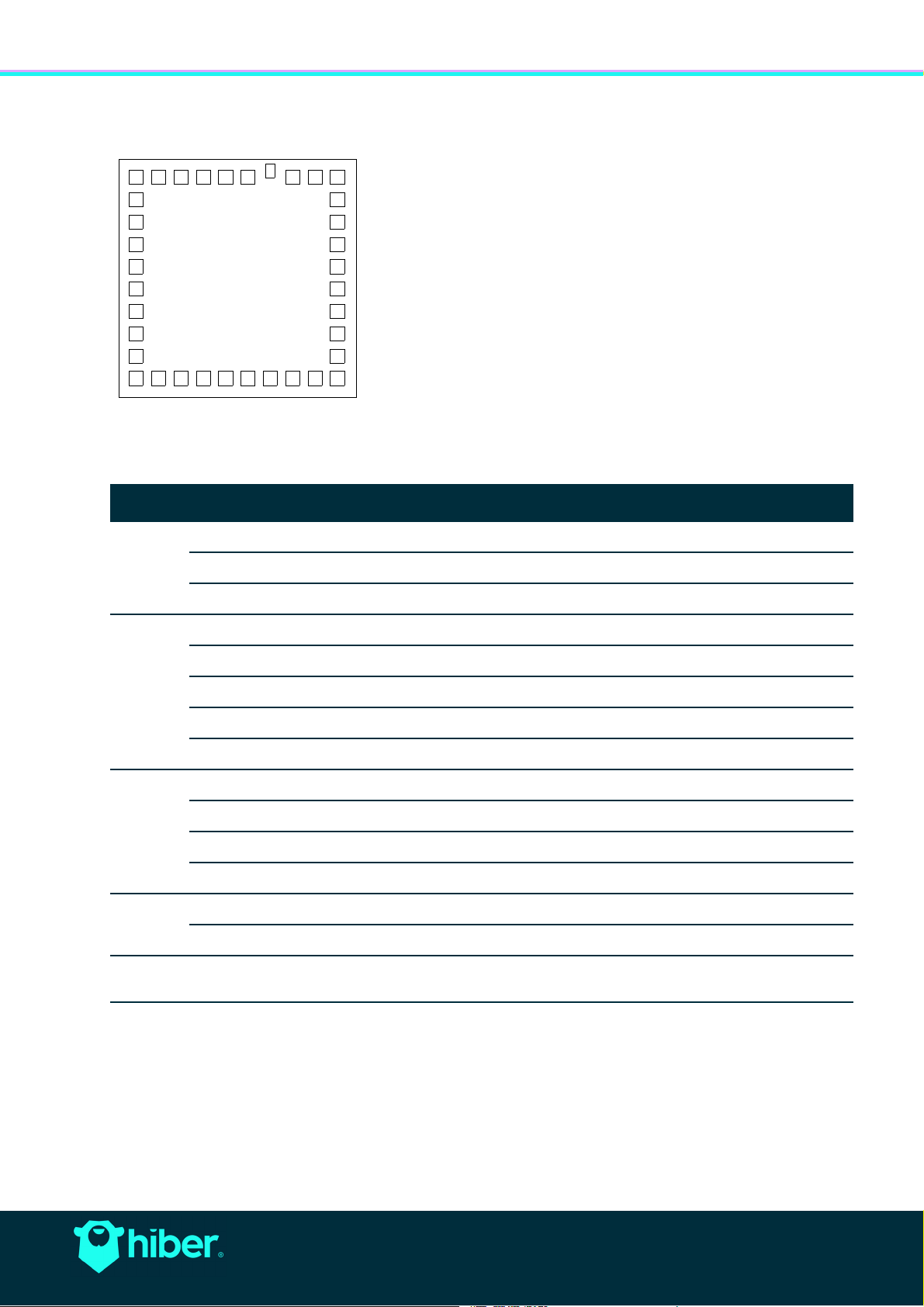
B1
C1
D1
E1
G1
F1
H1
J1
A1 A2 A3 A4 A5 A6
A7
A8 A9 A10
K1 K2 K3 K4 K5 K6 K7 K8 K9 K10
B10
C10
D10
E10
G10
F10
H10
J10
1 Hiberband modem pin-assignment
The pin numbering scheme of the Hiberband LPGAN modem (bottom
view) is shown in figure 1. The module footprint is a Land Grid Array (LGA)
that allows soldering onto a printed circuit board (PCB) using standard
reflow manufacturing techniques.
The pin function assignment is given in table 1.
Figure 1: Hiberband modem pin numbering scheme
Page 2
Function Pin name I/O Description Hiberband modem pin numbers
Power/RF VCC I Supply voltage A1, A2, B1, B10
GND n/a Ground A3, A4, A5, A6, A8, A9, A10, E10, K3, K6, K7, K10
ANTENNA n/a Hiberband antenna A7
System HOST_RXD I Host UART receive K4
HOST_TXD O Host UART transmit K5
WKUPn I System wake-up F1
RESETn I System reset J10
IRQn O System interrupt request D10
GNSS
GNSS_EN O GNSS module enable G1
GNSS_TP O GNSS module time pulse E1
GNSS_RXD I GNSS UART receive H1
GNSS_TXD O GNSS UART transmit J1
Debug DBG_RXD I Debug UART receive K9
DBG_TXD O Debug UART transmit K8
Reserved - n/a Reserved for internal or future use.
Table 1: Hiberband modem pin assignment overview
C1, C10, D1, F10, G10, H10, K1, K2
Leave unconnected!
Same world, different angle.
Copyright © 2019 - Hiber | www.hiber.global
Page 3
HBR-DS-19001: Hiberband modem product datasheet
2 Product specifications
Stressing the Hiberband modem above one or more of the ratings listed in the Absolute
Maximum Ratings section may cause permanent damage. These are stress ratings only.
Operating the Hiberband modem at these or at any conditions other than those specified in
the Operating Conditions sections of the specification should be avoided. Exposure to
Absolute Maximum Rating conditions for extended periods may affect device reliability.
Operating conditions ranges define those limits within which the functionality of the device is
guaranteed.
Where application information is given, it is advisory only and does not form part of the
specification.
Unless otherwise specified, all operating conditions are valid at an ambient operating temperature
of +25 °C.
2.1 Absolute maximum ratings
The absolute maximum ratings of the Hiberband modem given in table 2 apply over the operating temperature
range (for reasons of brevity the acronym HB is used for ’Hiberband’).
Page 3
Parameter Description Condition Min Max Unit
VCC Supply voltage DC voltage at VCC pins -0.3 4.0 V
WKUP WKUP input voltage DC voltage at WKUP pin -0.3 4.0 V
RESET RESET input voltage DC voltage at RESET pin -0.3 4.0 V
UART UART input voltages DC voltage at RXD pins -0.3 4.0 V
HB antenna power Input RF power at HB antenna -8 dBm
HB antenna ruggedness Output RF load mismatch at HB antenna 20:1 VSWR
T
storage
Table 2: Absolute maximum ratings
Storage temperature -40 +85 °C
The Hiberband modem is not protected against overvoltages or reversed voltages. If
necessary, voltage spikes exceeding the power supply voltage specification as given in the
table above must be limited to values within the specified boundaries by using appropriate
protection measures.
2.2 Operating temperature ranges
The following temperature ranges are defined for operation of the Hiberband modem:
• Normal operating temperature: the Hiberband modem is fully functional and meets all its product
specifications across the specified temperature range.
• Extended operating temperature: the Hiberband modem is fully functional but RF performance may be
degraded.
Same world, different angle.
Copyright © 2019 - Hiber | www.hiber.global
Page 4
HBR-DS-19001: Hiberband modem product datasheet
The environmental operating ranges of the Hiberband modem are defined in table 3.
Parameter Description Min Typ Max Unit
Page 4
T
operating
Table 3: Environmental conditions
Typical operating temperature +25 °C
Normal operating temperature -30 +70 °C
Extended operating temperature -40 +85 °C
2.3 Maximum ESD ratings
The maximum ESD ratings of the Hiberband modem are specified in table 4.
Parameter Max Unit Remarks
ESD sensitivity for all pins except HB antenna 1000 V Human Body Model according to JESD22-A114
ESD sensitivity for HB antenna 1000 V Human Body Model according to JESD22-A114
ESD immunity for HB antenna 4000 V Contact Discharge according to IEC 61000-4-2
8000 V Air Discharge according to IEC 61000-4-2
Table 4: ESD ratings
The Hiberband modem is an Electrostatic Sensitive Device (ESD) and requires appropriate
precautions when handling.
2.4 Power supply
The power supply characteristics of the Hiberband modem are specified in table 5.
Parameter Description Min Typ Max Unit
VCC Module supply voltage 3.2 3.3 3.9 V
ICC
peak
Table 5: Power supply specifications
Module peak current consumption through all VCC pins,
during transmit burst at maximum power level, with a
matched antenna
Module peak current consumption through all VCC pins,
during transmit burst at maximum power level, with a
mismatched antenna
1.8 A
2.2 A
Same world, different angle.
Copyright © 2019 - Hiber | www.hiber.global
Page 5

HBR-DS-19001: Hiberband modem product datasheet
M
e
a
s
u
r
e
m
e
n
t
s
b
a
s
e
d
o
n
s
i
m
i
l
a
r
e
l
e
c
t
r
o
n
i
c
s
,
a
c
t
u
a
l
b
e
h
a
v
i
o
r
T
B
D
M
e
a
s
u
r
e
m
e
n
t
s
b
a
s
e
d
o
n
s
i
m
i
l
a
r
e
l
e
c
t
r
o
n
i
c
s
,
a
c
t
u
a
l
b
e
h
a
v
i
o
r
T
B
D
2.5 Current consumption
The current consumption figures of the Hiberband modem are specified in table 6.
Mode Condition Min Typ Max Unit
Hibernation Mode VCC = 3.3V 0.5 0.7 1.5 µA
Host Communication Mode VCC = 3.3V 10 20 25 mA
Geo-location Mode VCC = 3.3V TBD TBD TBD mA
Hiberband Listen Mode VCC = 3.3V; max. receive sensitivity 20 23 30 mA
Page 5
Hiberband Transmission Mode VCC = 3.3V; VREF = 3.0V; max. receive sensitivity and
output power
Table 6: Hiberband modem current consumption
100 1250 1500 mA
When designing the application power supply, attention must be paid to the transient behaviour of the Hiberband
modem current consumption when the transmitter power amplifier is turned on. In particular, the Hiberband
transmission burst current consumption (figure 2) pattern needs to be taken into account. For comparison
purposes, the current consumption for transmission of a continuous wave is shown in figure 3.
Figure 2: Hiberband transmission burst current consumption
Figure 3: Hiberband modem transmitter current consumption (continuous wave)
Both patterns were measured with the maximum +30 dBm transmission power.
Same world, different angle.
Copyright © 2019 - Hiber | www.hiber.global
Page 6

HBR-DS-19001: Hiberband modem product datasheet
2.6 Dynamic performance
The dynamic performance figures of the Hiberband modem are given in table 7.
Parameter Description Min Typ Max Unit
Page 6
T
GNSS
T
listen
T
transmit
Table 7: Hiberband modem dynamic performance
Duration for a GNSS fix TBD TBD TBD s
Hiberband listen period 10 80 120 s
Hiberband transmission burst duration 280 400 500 ms
2.7 UART communication
The communication parameters of both UARTs of the Hiberband modem are given in table 8.
Parameter Description Value Unit
UART
bitrate
UART
SDU
Table 8: UART communication parameters
Default UART bitrate (both UART interfaces) 115.2 kbps
Serial data format (databits, parity, stopbits) 8, no parity, 1 stopbit (8N1) n.a.
2.8 Hiberband RF communication
The frequency ranges of the Hiberband modem are given in table 9.
Parameter Min Max Unit Remarks
Hiberband frequency range Uplink 399.90 400.02 MHz
Downlink 400.15 401.00 MHz Only for Hiberband network management
Table 9: Hiberband modem RF frequency bands
The RF receiver sensitivity figures of the Hiberband modem are given in table 10.
Parameter Min Typ Max Unit Remarks
Hiberband receiver sensitivity TBD TBD TBD dBm 50 source
Table 10: Hiberband modem RF receiver sensitivity
The RF transmission output power figures of the Hiberband modem are given in table 11.
Parameter Min Max Unit Remarks
Hiberband receiver transmit power Normal TBD TBD dBm 50 load
Boost 20.0 31.7 dBm 50 load
Table 11: Hiberband modem RF output power
Copyright © 2019 - Hiber | www.hiber.global
Same world, different angle.
Page 7
HBR-DS-19001: Hiberband modem product datasheet
H
A
B
VREF
WKUP
SYS_TXD
SYS_RXD
RESET
TXD
RXD
GPIO
GPIO
VCC
+3.3V
VCC
+3.3V
host application
processor
DBG_TXD
DBG_RXD
Hiberband modem
optional
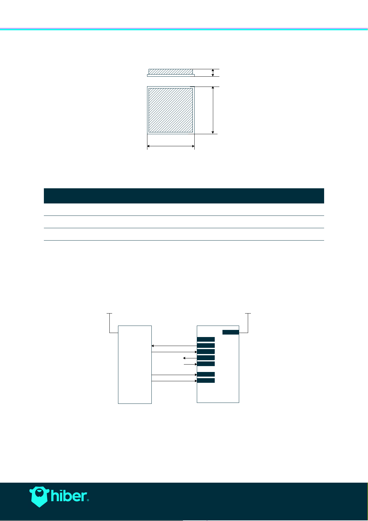
2.9 Mechanical dimensions
The mechanical drawing of the Hiberband modem is shown in figure 4.
Figure 4: Mechanical drawing Hiberband modem
The pin numbers have been omitted from figure 4. Please refer to section for pin assignment information.
Parameter Description Typical Tolerance
Page 7
A Module length 27.0 mm +0.2/-0.2 mm
B Module width 27.0 mm +0.2/-0.2 mm
H Module height 4.2 mm +0.3/-0.1 mm
Table 12: Module dimensions
The Hiberband modem an antenna pad for connection of an external antenna.
3 Typical application ciruit
A typical interface between the application host processor, generally a microcontroller, and the Hiberband
modem is shown in Figure 5.
Figure 5: Typical integration of a Hiberband modem with an application host processor
Copyright © 2019 - Hiber | www.hiber.global
Same world, different angle.
Page 8

HBR-DS-19001: Hiberband modem product datasheet
4 Hiberband modem design support
Hiber is strongly committed to providing good support to its partners. In addition to documentation, Hiber offers
CAD libraries, reference schematics and board layout footprints, that can be obtained upon request. Please
contact us at support@hiber.global for any assistance you may need.
5 Product ordering information
Please find the product ordering information in the table below.
Orderable device Status Description
HBR-19MDM001-001 Announced Hiberband modem, 2nd generation.
Table 13: Hiberband modem product ordering codes
6 Revision history
Page 8
Date Revision Changes
February 12, 2019 1.0 Initial document
March 19, 2019 1.1 Updated notices
Table 14: Document revision history
Same world, different angle.
Copyright © 2019 - Hiber | www.hiber.global
Page 9

HBR-DS-19001: Hiberband modem product datasheet
IMPORTANT NOTICES – PLEASE READ CAREFULLY
FCC Interference Statement, Part 15.105(b): This equipment has been tested and found to comply with the limits for a Class B digital
device, pursuant to Part 15 of the FCC Rules. These limits are designed to provide reasonable protection against harmful interference
in a residential installation. This equipment generates uses and can radiate radio frequency energy and, if not installed and used in
accordance with the instructions, may cause harmful interference to radio communications. However, there is no guarantee that
interference will not occur in a particular installation. If this equipment does cause harmful interference to radio or television reception,
which can be determined by turning the equipment off and on, the user is encouraged to try to correct the interference by one of the
following measures:
• Reorient or relocate the receiving antenna.
• Increase the separation between the equipment and receiver.
• Connect the equipment into an outlet on a circuit different from that to which the receiver is connected.
• Consult the dealer or an experienced radio/TV technician for help.
FCC Part 15.21 Warning: Changes or modifications not expressly approved by the party responsible for compliance could void the
user's authority to operate the equipment.
FCC Part 15.19(a) Statement: This device complies with Part 15 of the FCC Rules. Operation is subject to the following two
conditions: (1) This device may not cause harmful interference, and (2) this device must accept any interference received, including
interference that may cause undesired operation.”
FCC/ISED RF Exposure Guidance Statement: In order to comply with FCC/ISED RF Exposure requirements, this device must be
installed to provide at least 30 cm separation from the human body at all times. Afin de respecter les exigences de la FCC/ISED
concernant l'exposition aux fréquences radio, ce système doit être installé pour assurer une séparation d'au moins 30 cm du corps
humain à tout instant.
Page 9
Hiber BV, operating under the Hiber brand name, and its subsidiaries (“Hiber”), reserve the right to make changes, corrections,
enhancements, modifications, and improvements to Hiber products and/or to this document at any time without notice. Purchasers
should obtain the latest relevant information on Hiber products before placing orders. Hiber products are sold pursuant to Hiber’s
terms and conditions of sale in place at the time of order acknowledgement.
Purchasers are solely responsible for the choice, selection, and use of Hiber products and Hiber assumes no liability for application
assistance or the design of Purchasers’ products.
No license, express or implied, to any intellectual property right is granted by Hiber herein.
Resale of Hiber products with provisions different from the information set forth herein shall void any warranty granted by Hiber for
such product. Hiber and the Hiber logo are trademarks of Hiber BV. All other product or service names are the property of their
respective owners.
Information in this document supersedes and replaces information previously supplied in any prior versions of this document.
Company contact details can be found on Hiber’s corporate website at www.hiber.global.
Same world, different angle.
Copyright © 2019 - Hiber | www.hiber.global
 Loading...