

Page 1
5K250 SATA OEM Specificat ion
Hitachi Global Storage Technologies
Hard Disk Drive Specification
Hitachi Travelstar 5K250
2.5 inch SATA hard disk drive
Models: HTS542525K9A300, HTS542525K9SA00
HTS542516K9A300, HTS542516K9SA00
HTS542512K9A300, HTS542512K9SA00
HTS542580K9A300, HTS542580K9SA00
Revision 1.0 05 June 2007
Page 1 of 171
Page 2

5K250 SATA OEM Specificat ion
Preliminary Edition (Revision 0.1) (24 May 2007)
nd
2
Preliminary Edition (Revision 0.2) (29 May 2007)
Formal Release (Revision 1.0) (05 June 2007)
The following paragraph does not apply to the United Kingdom or any country where such
provisions are inconsistent with local law: HITACHI GLOBAL STORAGE TECHNOLOGIES
PROVIDES THIS PUBLICATION "AS IS" WITHOUT WARRANTY OF ANY KIND, EITHER
EXPRESS OR IMPLIED, INCLUDING, BUT NOT LIMITED TO, THE IMPLIED WARRANTIES
OF MERCHANTABILITY OR FITNESS FOR A PARTICULAR PURPOSE. Some states do not allow
disclaimer or express or implied warranties in certain transactions, therefore, this statement may
not apply to you.
This publication could include technical inaccuracies or typographical errors. Changes are
periodically made to the information herein; these changes will be incorporated in new editions of
the publication. Hitachi may make improvements or changes in any products or programs described
in this publication at any time.
It is possible that this publication may contain reference to, or information about, Hitachi products
(machines and programs), programming, or services that are not announced in your country. Such
references or information must not be construed to mean that Hitachi intends to announce such
Hitachi products, programming, or services in your country.
Technical information about this product is available by contacting your local Hitachi Global Storage
Technologies representative or on the Internet at http://www.hitachigst.com
Hitachi Global Storage Technologies may have patents or pending patent applications covering
subject matter in this document. The furnishing of this document does not give you any license to
these patents.
©Copyright Hitachi Global Storage Technologies
Note to U.S. Government Users —Documentation related to restricted rights —Use, duplication or
disclosure is subject to restrictions set forth in GSA ADP Schedule Contract with Hitachi Global
Storage Technologies.
Page 2 of 171
Page 3

5K250 SATA OEM Specificat ion
Table of Contents
GENERAL ............................................................................................................................................. 8
1 INTRODUCTION.....................................................................................................................................8
1.1 Abbreviations .......................................................................................................................... 8
1.2 References .............................................................................................................................11
1.3 General caution..................................................................................................................... 11
1.4 Drive handling precautions .................................................................................................. 11
2 OUTLINE OF THE DRIVE ...................................................................................................................... 12
PART 1 FUNCTIONAL SPECIFICATION ......................................................................................... 13
3 FIXED DISK SUBSYSTEM DESCRIPTION ................................................................................................14
3.1 Control Electronics................................................................................................................14
3.2 Head disk assembly data......................................................................................................14
4 FIXED DISK CHARACTERISTICS ........................................................................................................... 15
4.1 Formatted capacity by model number..................................................................................15
4.2 Data sheet .............................................................................................................................16
4.3 Cylinder allocation................................................................................................................ 16
4.4 Performance characteristics .................................................................................................17
5 DATA INTEGRITY ................................................................................................................................21
5.1 Data loss on power off ...........................................................................................................21
5.2 Write Cache........................................................................................................................... 21
5.3 Equipment status.................................................................................................................. 21
5.4 WRITE safety........................................................................................................................21
5.5 Data buffer test.....................................................................................................................22
5.6 Error recovery ....................................................................................................................... 22
5.7 Automatic reallocation..........................................................................................................22
5.8 ECC .......................................................................................................................................23
6 SPECIFICATION .................................................................................................................................. 24
6.1 Environment .........................................................................................................................24
6.2 DC power requirements........................................................................................................ 26
6.3 Reliability..............................................................................................................................28
6.4 Mechanical specifications ..................................................................................................... 31
6.5 Vibration and shock..............................................................................................................33
6.6 Acoustics................................................................................................................................ 35
6.7 Identification labels .............................................................................................................. 36
6.8 Electromagnetic compatibility.............................................................................................. 36
6.9 Safety..................................................................................................................................... 37
6.10 Packaging .............................................................................................................................. 37
6.11 Substance restriction requirements .....................................................................................37
7 ELECTRICAL INTERFACE SPECIFICATIONS ..........................................................................................38
7.1 Cabling .................................................................................................................................. 38
7.2 Interface connector................................................................................................................ 38
7.3 Signal definitions .................................................................................................................. 39
PART 2 INTERFACE SPECIFICATION ............................................................................................ 41
8 GENERAL ........................................................................................................................................... 42
8.1 Introduction...........................................................................................................................42
8.2 Terminology........................................................................................................................... 42
9 DEVIATIONS FROM STANDARD............................................................................................................ 43
10 PHYSICAL INTERFACE ......................................................................................................................43
11 REGISTERS ....................................................................................................................................... 43
11.1 Register naming convention.................................................................................................44
11.2 Command register.................................................................................................................44
11.3 Device Control Register ........................................................................................................44
11.4 Device Register...................................................................................................................... 45
11.5 Error Register .......................................................................................................................45
Page 3 of 171
Page 4

5K250 SATA OEM Specificat ion
11.6 Features Register..................................................................................................................45
11.7 LBA High Register................................................................................................................ 45
11.8 LBA Low Register .................................................................................................................46
11.9 LBA Mid Register .................................................................................................................46
11.10 Sector Count Register........................................................................................................ 46
11.11 Status Register .................................................................................................................. 46
12 GENERAL OPERATION DESCRIPTIONS ..............................................................................................48
12.1 Reset Response...................................................................................................................... 48
12.2 Diagnostic and Reset considerations....................................................................................49
12.3 Power-off considerations.......................................................................................................50
12.4 Sector Addressing Mode........................................................................................................51
12.5 Power Management Feature ................................................................................................51
12.6 Advanced Power Management (Adaptive Battery Life Extender 3) Feature .....................53
12.7 Interface Power Management Mode (Slumber and Partial)................................................ 54
12.8 S.M.A.R.T. Function .............................................................................................................54
12.9 Security Mode Feature Set...................................................................................................55
12.10 Protected Area Function ................................................................................................... 61
12.11 Seek Overlap...................................................................................................................... 64
12.12 Write Cache Function........................................................................................................ 64
12.13 Reassign Function ............................................................................................................. 64
12.14 48-bit Address Feature Set ............................................................................................... 65
12.15 Software Setting Preservation Feature Set...................................................................... 66
12.16 Native Command Queuing................................................................................................ 67
12.17 SMART Command Transport (SCT)................................................................................. 67
13 COMMAND PROTOCOL ...................................................................................................................... 69
13.1 Data In Commands...............................................................................................................69
13.2 Data Out Commands ............................................................................................................ 69
13.3 Non-Data Commands............................................................................................................ 70
13.4 DMA Data Transfer Commands........................................................................................... 71
13.5 First-parity DMA Commands...............................................................................................71
14 COMMAND DESCRIPTIONS ................................................................................................................ 72
14.1 Check Power Mode (E5h/98h)............................................................................................... 76
14.2 Device Configuration Overlay (B1h) .................................................................................... 77
14.3 Execute Device Diagnostic (90h) ..........................................................................................81
14.4 Flush Cache (E7h)................................................................................................................. 82
14.5 Flush Cache Ext (EAh) ......................................................................................................... 83
14.6 Format Track (50h: Vendor Specific) ................................................................................... 84
14.7 Format Unit (F7h: Vendor Specific) .....................................................................................85
14.8 Identify Device (ECh)............................................................................................................86
14.9 Idle (E3h/97h)........................................................................................................................97
14.10 Idle Immediate (E1h/95h) ................................................................................................. 98
14.11 Initialize Device Parameters (91h) ...................................................................................99
14.12 Read Buffer (E4h)............................................................................................................ 100
14.13 Read DMA(C8h/C9h)....................................................................................................... 101
14.14 Read DMA Ext (25h) ....................................................................................................... 102
14.15 Read FPDMA Queued (60h)............................................................................................103
14.16 Read Log Ext(2Fh)........................................................................................................... 104
14.17 Read Multiple (C4h) ........................................................................................................ 112
14.18 Read Multiple Ext (29h).................................................................................................. 113
14.19 Read Native Max Address (F8h)..................................................................................... 114
14.20 Read Native Max Address Ext (27h)............................................................................... 115
14.21 Read Sector(s) (20h/21h) ................................................................................................. 116
14.22 Read Sector(s) Ext (24h).................................................................................................. 117
14.23 Read Verify Sector(s) (40h/41h) ......................................................................................118
14.24 Read Verify Sector(s) Ext (42h)....................................................................................... 119
14.25 Recalibrate (1xh) ............................................................................................................. 120
14.26 Security Disable Password (F6h)....................................................................................121
14.27 Security Erase Prepare (F3h) ......................................................................................... 122
14.28 Security Erase Unit (F4h)............................................................................................... 123
Page 4 of 171
Page 5

5K250 SATA OEM Specificat ion
14.29 Security Freeze Lock (F5h) ............................................................................................. 125
14.30 Security Set Password (F1h)........................................................................................... 126
14.31 Security Unlock (F2h) .....................................................................................................128
14.32 Seek (7xh) ........................................................................................................................129
14.33 Sense Condition (F0h : vendor specific).......................................................................... 130
14.34 Set Features (EFh) .......................................................................................................... 131
14.35 Set Max Address (F9h).................................................................................................... 133
14.36 Set Max Address Ext (37h) ............................................................................................. 135
14.37 Set Multiple (C6h) ........................................................................................................... 137
14.38 Sleep (E6h/99h)................................................................................................................ 138
14.39 S.M.A.R.T Function Set (B0h)......................................................................................... 139
14.40 Standby (E2h/96h)........................................................................................................... 154
14.41 Standby Immediate (E0h/94h)........................................................................................ 155
14.42 Write Buffer (E8h)........................................................................................................... 156
14.43 Write DMA (CAh/CBh).................................................................................................... 157
14.44 Write DMA Ext (35h) ...................................................................................................... 158
14.45 Write DMA FUA Ext (3Dh)............................................................................................. 159
14.46 Write FPDMA Queued (61h)........................................................................................... 160
14.47 Write Log Ext (3Fh)......................................................................................................... 161
14.48 Write Multiple (C5h) ....................................................................................................... 162
14.49 Write Multiple Ext (39h)................................................................................................. 163
14.50 Write Multiple FUA Ext (CEh) .......................................................................................164
14.51 Write Sector(s) (30h/31h) ................................................................................................165
14.52 Write Sector(s) Ext (34h)................................................................................................. 166
14.53 Write Uncorrectable Ext (45h)........................................................................................167
15 TIMINGS ......................................................................................................................................... 169
List of Figures
Figure 1. Limits of temperature and humidity 24
Figure 2. Mounting hole locations 31
Figure 3. Interface connector pin assignments 38
Figure 4. Parameter descriptions 40
Figure 5 Initial Setting 57
Figure 6 Usual Operation 58
Figure 7 Password Lost 59
Figure 8 Set Max security mode transition 63
Figure 9 Seek overlap 64
Figure 10 Selective self-test test span example 141
List of Tables
Table 1. Formatted capacity by model number. 15
Table 2. Data sheet 16
Table 3. Cylinder allocation 16
Table 4. Performance characteristics 17
Table 5. Mechanical positioning performance 18
Table 6. Full stroke seek time 18
Table 7. Single track seek time 18
Table 8. Latency time 18
Table 9. Drive ready time 19
Table 10. Operating mode 20
Table 11. Drive rea dy time 20
Table 12. Environmental condition 24
Table 13. Magnetic flux density limits 25
Table 14. DC Power requirements 26
Table 15. Power consumption efficiency 27
Table 16. Physical dimensions and weight 31
Page 5 of 171
Page 6

5K250 SATA OEM Specificat ion
Table 17. Random vibration PSD profile breakpoints (operating) 33
Table 18. Swept sine vibration 33
Table 19. Random Vibration PSD Profile Breakpoints (nonoperating) 34
Table 20. Operating shock 34
Table 21. Nonoperating shock 34
Table 22. Weighted sound power 35
Table 23. Interface connector pins and I/O signa ls 39
Table 24 Register naming convention and correspondence 44
Table 25 Device Control Register 44
Table 26 Device Register 45
Table 27 Error Register 45
Table 28 Status Register 46
Table 29 Reset Response Table 48
Table 30 Default Register Values 49
Table 31 Diagnostic Codes 49
Table 32 Reset error register values 49
Table 33 Device’s behavior by ATA commands 50
Table 34 Power conditions 52
Table 35 Command table for device lock operation 60
Table 36 Command table for device lock operation - continued 61
Table 37 Set Max Set Password data content 63
Table 38 Preserved Software Setting 67
Table 39 SCT Action Code Supported 68
Table 40 Command set 72
Table 41 Command Set - continued 73
Table 42 Command Set (Subcommand) 74
Table 43 Check Power Mode Command (E5h/98h) 76
Table 44 Device Configuration Overlay Command (B1h) 77
Table 45 Device Configuration Overlay Features register values 77
Table 46 Device Configuration Overlay Data structure 79
Table 47 DCO error information definition 80
Table 48 Execute Device Diagnostic Command (90h) 81
Table 49 Flush Cache Command (E7h) 82
Table 50 Flush Cache EXT Command (EAh) 83
Table 51 Format Track Command (50h) 84
Table 52 Format Unit Command (F7h) 85
Table 53 Identify Device Command (ECh) 86
Table 54 Identify device information 87
Table 55 Identify device information --- Continued --- 88
Table 56 Identify device information --- Continued --- 89
Table 57 Identify device information --- Continued --- 90
Table 58 Identify device information --- Continued --- 91
Table 59 Identify device information --- Continued --- 92
Table 60 Identify device information --- Continued --- 93
Table 61 Identify device information --- Continued --- 94
Table 62 Identify device information --- Continued --- 95
Table 63 Number of cylinders/heads/sectors by models for HTS5425XXK9SA00 / HTS5425XXK9A300 96
Table 64 Idle Command (E3h/97h) 97
Table 65 Idle Immediate Command (E1h/95h) 98
Table 66 Initialize Device Parameters Command (91h) 99
Table 67 Read Buffer Command (E4h) 100
Table 68 Read DMA Command (C8h/C9h) 101
Table 69 Read DMA Ext Command (25h) 102
Table 70 Read FPDMA Queued Command (60h) 103
Table 71 Read Log Ext Command (2Fh) 104
Table 72 Log address definition 104
Table 73 General purpose Log Directory 105
Table 74 Extended comprehensive SMART error Log 106
Table 75 Extended Error log data structure 106
Table 76 Command data structure 107
Table 77 Error data structure 107
Table 78 Extended Self-test log data structure 108
Page 6 of 171
Page 7

5K250 SATA OEM Specificat ion
Table 79 Extended Self-test log descriptor entry 109
Table 80 Command Error information 109
Table 81 Phy Event Counter Identifier 110
Table 82 Phy Event Counter information 111
Table 83 Read Multiple Command (C4h) 112
Table 84 Read Multiple Ext Command (29h) 113
Table 85 Read Native Max Address Command (F8h) 114
Table 86 Read Native Max Address Ext Command (29h) 115
Table 87 Read Sector(s) Command (20h/21h) 116
Table 88 Read Sector(s) Ext Command (24h) 117
Table 89 Read Verify Sector(s) Command (40h/41h) 118
Table 90 Read Verify Sector(s) Ext Command (42h) 119
Table 91 Recalibrate Command (1xh) 120
Table 92 Security Disable Password Command (F6h) 121
Table 93 Password Information for Security Disable Password command 121
Table 94 Security Erase Prepare Command (F3h) 122
Table 95 Security Erase Unit Command (F4h) 123
Table 96 Erase Unit Information 123
Table 97 Security Freeze Lock Command (F5h) 125
Table 98 Security Set Password Command (F1h) 126
Table 99 Security Set Password Information 126
Table 100 Security Unlock Command (F2h) 128
Table 101 Security Unlock Information 128
Table 102 Seek Command (7xh) 129
Table 103 Sense Condition Command (F0h) 130
Table 104 Set Features Command (EFh) 131
Table 105 Set Max Address Command (F9h) 133
Table 106 Set Max Address Ext Command (37h) 135
Table 107 Set Multiple Command (C6h) 137
Table 108 Sleep Command (E6h/99h) 138
Table 109 S.M.A.R.T. Function Set Command (B0h) 139
Table 110 Log sector addresses 142
Table 111 Device Attribute Data Structure 144
Table 112 Individual Attribute Data Structure 145
Table 113 Status Flag Definitions 146
Table 114 Device Attribute Thresholds Data Structure 148
Table 115 Individual Threshold Data Structure 149
Table 116 SMART Log Directory 149
Table 117 S.M.A.R.T. error log sector 150
Table 118 Error log data structure 150
Table 119 Command data structure 151
Table 120 Error data structure 151
Table 121 Self-test log data structure 152
Table 122 Selective self-test log data structure 153
Table 123 S.M.A.R.T. Error Codes 153
Table 124 Standby Command (E2h/96h) 154
Table 125 Standby Immediate Command (E0h/94h) 155
Table 126 Write Buffer Command (E8h) 156
Table 127 Write DMA Command (CAh/CBh) 157
Table 128 Write DMA Ext Command (35h) 158
Table 129 Write DMA FUA Ext Command (3Dh) 159
Table 130 Write FPDMA Queued Command (61h) 160
Table 131 Write Log Ext Command 161
Table 132 Write Multiple Command (C5h) 162
Table 133 Write Multiple Ext Command (39h) 16 3
Table 134 Write Multiple FUA Ext Command (CEh) 164
Table 135 Write Sector(s) Command (30h/31h) 165
Table 136 Write Sector(s) Ext Command (34h) 166
Table 137 Write Uncorrectable Ext Command (45h) 167
Table 138 Timeout Values 169
Page 7 of 171
Page 8
5K250 SATA OEM Specificat ion
General
1 Introduction
This document describes the specifications of the HITACHI Travelstar 5K250, a 2.5-inch hard disk
drive with Serial ATA interface:
Drive
name
Travelstar
5K250-250
Travelstar
5K250-160
Travelstar
5K250-120
Travelstar
5K250-80
Part 1 of this document beginning on page 14 defines the hardware functional specification. Interface
specification is separately issued.
Model Number Max data
transfer rate
(Gbps)
HTS542525K9A300 3.0
HTS542525K9SA00 1.5
HTS542516K9A300 3.0
HTS542516K9SA00 1.5
HTS542512K9A300 3.0
HTS542512K9SA00 1.5
HTS542580K9A300 3.0
HTS542580K9SA00 1.5
Capacity
(GB)
250 9.5 5400
160 9.5 5400
120 9.5 5400
80 9.5 5400
Height (mm) Rotation
speed (rpm)
1.1 Abbreviations
Abbreviation Meaning
32 KB 32 x 1024 bytes
64 KB 64 x 1024 bytes
“ inch
A amp
AC alternating current
AT Advanced Technology
ATA Advanced Technology Attachment
Bels unit of sound power
BIOS Basic Input/Output System
°C degrees Celsius
CSA Canadian Standards Association
C-UL Canadian-Underwriters Laboratory
Cyl cylinder
DC direct current
DFT Drive Fitness Test
DMA Direct Memory Access
ECC error correction code
EEC European Economic Community
Page 8 of 171
Page 9

EMC electromagnetic compatibility
ERP Error Recovery Procedure
Esd electrostatic discharge
FCC Federal Communications Commission
FRU field replacement unit
G gravity, a unit of force
Gb 1 000 000 000 bits
GB 1 000 000 000 bytes
GND ground
h hexadecimal
HDD hard disk drive
Hz hertz
I Input
ILS integrated lead suspension
imped impedance
I/O Input/Output
ISO International Standards Organization
KB 1,000 bytes
5K250 SATA OEM Specificat ion
Kbit/mm 1,000 bits per mm
Kbit/sq-mm 1000 bits per square mm
KHz kilohertz
LBA logical block addressing
Lw unit of A-weighted sound power
m meter
max. or Max. maximum
MB 1,000,000 bytes
Mbps 1,000,000 Bit per second
Mb/sec 1,000,000 Bit per second
MB/sec 1,000,000 bytes per second
MHz megahertz
MLC Machine Level Control
mm millimeter
ms millisecond
us, s microsecond
Nm Newton meter
No. or # number
oct/min oscillations per minute
O Output
OD Open Drain Programmed Input/Output
Page 9 of 171
Page 10

PIO
POH power on hours
Pop. population
P/N part number
p-p peak-to-peak
PSD power spectral density
RES radiated electromagnetic susceptibility
RFI radio frequency interference
RH relative humidity
% RH per cent relative humidity
RMS root mean square
RPM revolutions per minute
RST reset
R/W read/write
sec second
Sect/Trk sectors per track
SELV secondary low voltage
S.M.A.R.T Self-monitoring, analysis, and reporting technology
5K250 SATA OEM Specificat ion
Trk. track
TTL transistor-transistor logic
UL Underwriters Laboratory
V volt
VDE Verband Deutscher Electrotechniker
W watt
3-state transistor-transistor tristate logic
Page 10 of 171
Page 11

5K250 SATA OEM Specificat ion
1.2 References
Serial ATA International Organization : Serial ATA Revision 2.6
1.3 General caution
Do not apply force to the top cover (See figure below).
Do not cover the breathing hole on the top cover (See figure below).
Do not touch the interface connector pins or the surface of the printed circuit board.
The drive can be damaged by shock or ESD (Electric Static Discharge). Any damages incurred to
the drive after removing it from the shipping package and the ESD protective bag are the
responsibility of the user
1.4 Drive handling precautions
Do not press on the drive cover during handling.
Page 11 of 171
Page 12

5K250 SATA OEM Specificat ion
2 Outline of the drive
2.5-inch, 9.5-mm Height
Perpendicular Recording
Formatted capacities of 250GB, 160GB,120GB, and 80GB (512 bytes/sector)
SATA Interface conforming to Serial ATA International Organization: Serial ATA Revision
2.6(15-February-2007)
Integrated controller
No-ID recording format
Coding : 100/102 2bit parity (199/200 RC Modulation Encoding)
Multi zone recording
Enhanced
10 bit 40 symbol non Interleaved Read Solomon code
Non interleave On-The –Fly correction
Included 2 symbol system ECC
Segmented Buffer with write cache
8192 KB - Upper 736 KB is used for firmware
Fast data transfer rate
HTS5425xxK9A300 model : up to 3.0Gbit/s
HTS5425xxK9SA00 model : up to 1.5Gbit/s
Media data transfer rate (max):
665 Mb/s
Average seek time: 11 ms for read
Closed-loop actuator servo (Embedded Sector Servo)
Rotary voice coil motor actuator
Load/Unload mechanism
Mechanical latch
0.55 Watts at idle state
ECC
Power on to ready
3.5 sec
Operating shock
3920 m/sec2 (400 G)/2ms
1960 m/sec2 (200G)/1ms
Nonoperating shock
9800 m/sec2 (1000 G)/1ms
Full data encryption as optional (HTS5425xxK9SA00 model only)
Page 12 of 171
Page 13

Part 1 Functional Specification
5K250 SATA OEM Specificat ion
Page 13 of 171
Page 14

5K250 SATA OEM Specificat ion
3 Fixed disk subsystem description
3.1 Control Electronics
The control electronics works with the following functions:
SATA Interface Protocol
Embedded Sector Servo
No-ID (TM) formatting
Multizone recording
Code: 100/102 bit parity (199/200 RC Modulation Encoding)
System ECC
Enhanced Adaptive Battery Life Extender
3.2 Head disk assembly data
The following technologies are used in the drive:
Femto Slider
Perpendicular recording disk and write head
TMR head
Integrated lead suspension (ILS)
Load/unload mechanism
Mechanical latch
Page 14 of 171
Page 15
5K250 SATA OEM Specificat ion
4 Fixed disk characteristics
4.1 Formatted capacity by model number
Description
Physical Layout
Bytes per Sector 512 512 512 512
Number of Heads 4 3 2 2
Number of Disks 2 2 1 1
Logical Layout
Number of Heads 16 16 16 16
Number of Sectors/
Track
Number of
Cylinders
Number of Sectors 488,397,168 312,581,808 234,441,648 156,301,488
Total Logical Data
Bytes
Table 1. Formatted capacity by model number.
HTS542525K9A300
HTS542525K9SA00
63 63 63 63
16,383 16,383 16,383 16,383
250,059,350,016 160,041,885,696 120,034,123,776 80,026,361,856
HTS542516K9A300
HTS542516K9SA00
HTS542512K9A300
HTS542512K9SA00
HTS542580K9A300
HTS542580K9SA00
Page 15 of 171
Page 16
5K250 SATA OEM Specificat ion
4.2 Data sheet
250GB 160GB 120GB 80GB
Rotational S p ee d (R P M ) 5400 5400 5400 5400
Data transfer rates (buffer to/from
media) (Mbps)
Data transfer rates (Gbit/sec) 1.5/ 3.0 1.5/ 3.0 1.5/ 3.0 1.5/ 3.0
Recording density (Kbit/mm) (Max)
(KBPI) (Max)
Track density (Ktrack/mm)(Max)
(KTPI)(Max)
Areal density (Kbit/sq-mm.- Max)
(Gbit/sq-inch - Max)
Number of zones 24 24 24 24
665 619 643 530
1100
186
205
1035
172
192
1076
185
200
902
151
167
Table 2. Data sheet
4.3 Cylinder allocation
Data format is allocated by each head characteristics. Typical format is described below.
Zone
0 0 - 4535 1368
1 4536 - 12149 1344
2 12150 - 15146 1312
3 15147 - 18872 1296
4 18873 - 22598 1272
5 22599 - 28025 1248
6 28026 - 35396 1200
7 35397 - 39122 1176
8 39123 - 45926 1152
9 45927 - 49814 1120
10 49815 - 55322 1080
11 55323 - 60830 1056
12 60831 - 65771 1032
13 65772 - 70550 1008
14 70551 - 75167 984
15 75168 - 81404 960
16 81405 - 84401 928
17 84402 - 90233 896
18 90234 - 94931 864
19 94932 - 99224 832
20 99225 - 103517 800
21 103518 - 110240 768
22 110241 - 112103 736
23 112104 - 116558 704
125GB/p Mid BIP-Mid TPI format
Cylinder
No. of
Sectors/Trk
Table 3. Cylinder allocation
Page 16 of 171
Page 17

5K250 SATA OEM Specificat ion
4.4 Performance characteristics
Drive performance is characterized by the following parameters:
Command Overhead
Mechanical Positioning
Seek Time
Latency
Data Transfer Speed
Buffering Operation (Look ahead/Write Cache)
Note: All the above parameters contribute to drive performance. There are other parameters which
contribute to the performance of the actual system. This specification defines the essential characteristics
of the drive. This specification does not include the system throughput as this is dependent upon the
system and the application.
The following table gives a typical value for each parameter. The detailed descriptions are found in
section 5.0.
Function
Average Random Seek Time - Read (ms) 11
Average Random Seek Time - Write (ms) 13
Rotational S p ee d (R P M ) 5400
Power-on-to-ready (sec) 3.5
Command overhead (ms) 1.0
Disk-buffer data transfer (Mb/s) (max) 665
Buffer-host data transfer (Gbit/s) (max) 1.5 / 3.0
Table 4. Performance ch aracteristics
4.4.1 Command overhead
Command overhead time is defined as the interval from the time that a drive receives a command to the
time that the actuator starts its motion.
Page 17 of 171
Page 18
5K250 SATA OEM Specificat ion
4.4.2 Mechanical positioning
4.4.2.1 Average seek time (including settling)
Command Type Typical (ms) Max. (ms)
Read 11 14
Write 13 15
Table 5. Mechanical positioning performance
Typical and Max. are defined throughout the performance specification as follows:
Typical
Max.
The seek time is measured from the start of motion of the actuator to the start of a reliable read or write
operation. A reliable read or write operation implies that error correction/recovery is not employed to
correct arrival problems. The Average Seek Time is measured as the weighted average of all possible
seek combinations.
Σ (max. + 1 – n)(Tn
Weighted Average = ––––––––––––––––––––––––––––
(max. + 1)(max)
Where: max. = maximum seek length
n = seek length (1-to-max.)
Tn
Tn
Average of the drive population tested at nominal environmental and voltage conditions.
Maximum value measured on any one drive over the full range of the environmental and
voltage conditions. (See section 6.1, "Environment" on page 23 and section 6.2, "DC power
requirements" on page 25)
max.
in
out
+ Tn
n=1
= inward measured seek time for an n-track seek
= outward measured seek time for an n-track seek
in
out
)
4.4.2.2 Full stroke seek
Command Type Typical (ms) Max. (ms)
Read 20.0 25.0
Write 21.0 26.0
Table 6. Full stroke seek time
Full stroke seek time in milliseconds is the average time of 1000 full stroke seeks.
4.4.2.3 Single track seek time (without command overhead, including
settling)
Command Type Typical (ms) Maximum (ms)
Read 1.0 2.0
Write 1.1 2.2
Table 7. Single track seek time
Single track seek is measured as the average of one (1) single track seek from every track in both
directions (inward and outward).
4.4.2.4 Average latency
Rotational Speed
(RPM)
5400 11.1 5.5
Table 8. Latency time
Time for one revolution
(ms)
Average Latency
(ms)
Page 18 of 171
Page 19

4.4.2.5 Drive ready time
Condition Typical (sec) Max. (sec)
Power On To Ready 3.5 9.5
Table 9. Drive ready tim e
5K250 SATA OEM Specificat ion
Ready
Power On To Ready
The condition in which the drive is able to perform a media access command
(for example—read, write) immediately.
This includes the time required for the internal self diagnostics.
Page 19 of 171
Page 20
4.4.3 Operating modes
Operating mode Description
5K250 SATA OEM Specificat ion
Spin-Up
Seek
Write
Read
Performance
Active idle
Low power idle
Standby
Sleep
Table 10. Operating mode
Start up time period from spindle stop or power down.
Seek operat ion mode
Write operation mode
Read operation mode
The device is capable of responding immediately to idle media access requests. All
electronic components remain powered and the full frequency servo remains
operational.
The device is capable of responding immediately to media access requests. Some
circuitry—including servo system and R/W electronics—is in power saving mode.
The head is parked near the mid-diameter the disk without servoing.
A device in Active idle mode may take longer to complete the execution of a
command because it must activate that circuitry.
The head is unloaded onto the ramp position. The spindle motor is rotating at full
speed.
The device interface is capable of accepting commands. The spindle motor is
stopped. A ll circuitry but the host interface is in power saving mode.
The execution of commands is delayed until the spindle becomes ready.
The device requires a soft reset or a hard reset to be activated. All electronics,
including spindle motor and host interface, are shut off.
4.4.3.1 Mode transition time
From To Transition
Time (typ)
Standby Idle 2.5 9.5
Table 11. Drive ready time
Transition Time
(max.)
4.4.3.2 Operating mode at power on
The device goes into Idle mode after power on or hard reset as an initial state. Initial state may be
changed to Standby mode using pin C on the interface connector. Refer to section 7.10 on page 58,
"Drive address setting" for details.
4.4.3.3 Adaptive power save control
The transient timing from Performance Idle mode to Active Idle mode and Active Idle mode to Low Power
Idle mode is controlled adaptively according to the access pattern of the host system. The transient
timing from Low Power Idle mode to Standby mode is also controlled adaptively, if it is allowed by Set
Features Enable Advanced Power Management subcommand.
Page 20 of 171
Page 21

5K250 SATA OEM Specificat ion
5 Data integrity
5.1 Data loss on power off
Data loss will not be caused by a power off during any operation except the write operation.
A power off during a write operation causes the loss of any received or resident data that has not
been written onto the disk media.
A power off during a write operation might make a maximum of one sector of data unreadable. This
state can be recovered by a rewrite operation.
5.2 Write Cache
When the write cache is enabled, the write command may complete before the actual disk write operation
finishes. This means that a power off, even after the write command completion, could cause the loss of
data that the drive has received but not yet written onto the disk.
In order to prevent this data loss, confirm the completion of the actual write operation prior to the power
off by issuing a
Soft reset
Hard reset
Flush Cache command
Standby command
Standby Immediate command
Sleep command
Confirm the command’s completion.
5.3 Equipment status
The equipment status is available to the host system any time the drive is not ready to read, write, or seek.
This status normally exists at the power-on time and will be maintained until the following conditions are
satisfied:
The access recalibration/tuning is complete.
The spindle speed meets the requirements for reliable operation.
The self-check of the drive is complete.
The appropriate error status is made available to the host system if any of the following conditions occur
after the drive has become ready:
The spindle speed lies outside the requirements for reliable operation.
The occurrence of a Write Fault condition.
5.4 WRITE safety
The drive ensures that the data is written into the disk media properly. The following conditions are
monitored during a write operation. When one of these conditions exceeds the criteria, the write operation
is terminated and the automatic retry sequence is invoked.
Head off track
External shock
Low supply voltage
Spindle speed out of tolerance
Head open/short
Page 21 of 171
Page 22

5K250 SATA OEM Specificat ion
5.5 Data buffer test
The data buffer is tested at power on reset and when a drive self-test is requested by the host. The test
consists of a write/read '00'x and 'ff'x pattern on all buffers.
5.6 Error recovery
Errors occurring on the drive are handled by the error recovery procedure.
Errors that are uncorrectable after application of the error recovery procedure are reported to the host
system as nonrecoverable errors.
5.7 Automatic reallocation
The sectors that show some errors may be reallocated automatically when specific conditions are met.
The drive does not report any auto reallocation to the host system. The conditions for auto reallocation
are described below.
5.7.1 Nonrecovered write errors
When a write operation cannot be completed after the Error Recovery Procedure (ERP) is fully carried out,
the sectors are reallocated to the spare location. An error is reported to the host system only when the
write cache is di s a bl ed and the auto realloc at i on h a s fai led.
5.7.2 Nonrecoverable read error
When a read operation fails after ERP is fully carried out, a hard error is reported to the host system. This
location is registered internally as a candidate for the reallocation. When a registered location is specified
as a target of a write operation, a sequence of media verification is performed automatically. When the
result of this verification meets the required criteria, this sector is reallocated.
5.7.3 Recovered read errors
When a read operation for a sector fails and is recovered at the specific ERP step, the sector is
reallocated automatically. A media verification sequence may be run prior to the reallocation according to
the predefined conditions.
Page 22 of 171
Page 23

5K250 SATA OEM Specificat ion
5.8 ECC
The 10 bit 40 symbol non interleaved ECC processor provides user data verification and correction
capability. The first 6 symbol of ECC are 4 check symbols for user data and the 2 symbol system ECC.
The other 34 symbols are Read Solomon ECC. Hardware logic corrects up to 16 symbols(20 bytes)
errors on-th e- fly.
2 symbol System ECC is generated when HDC receives user data from HOST, and can correct up to 1
symbol(10bit) errors on- the-fly when on e transfers to HOST.
Page 23 of 171
Page 24
5K250 SATA OEM Specificat ion
6 Specification
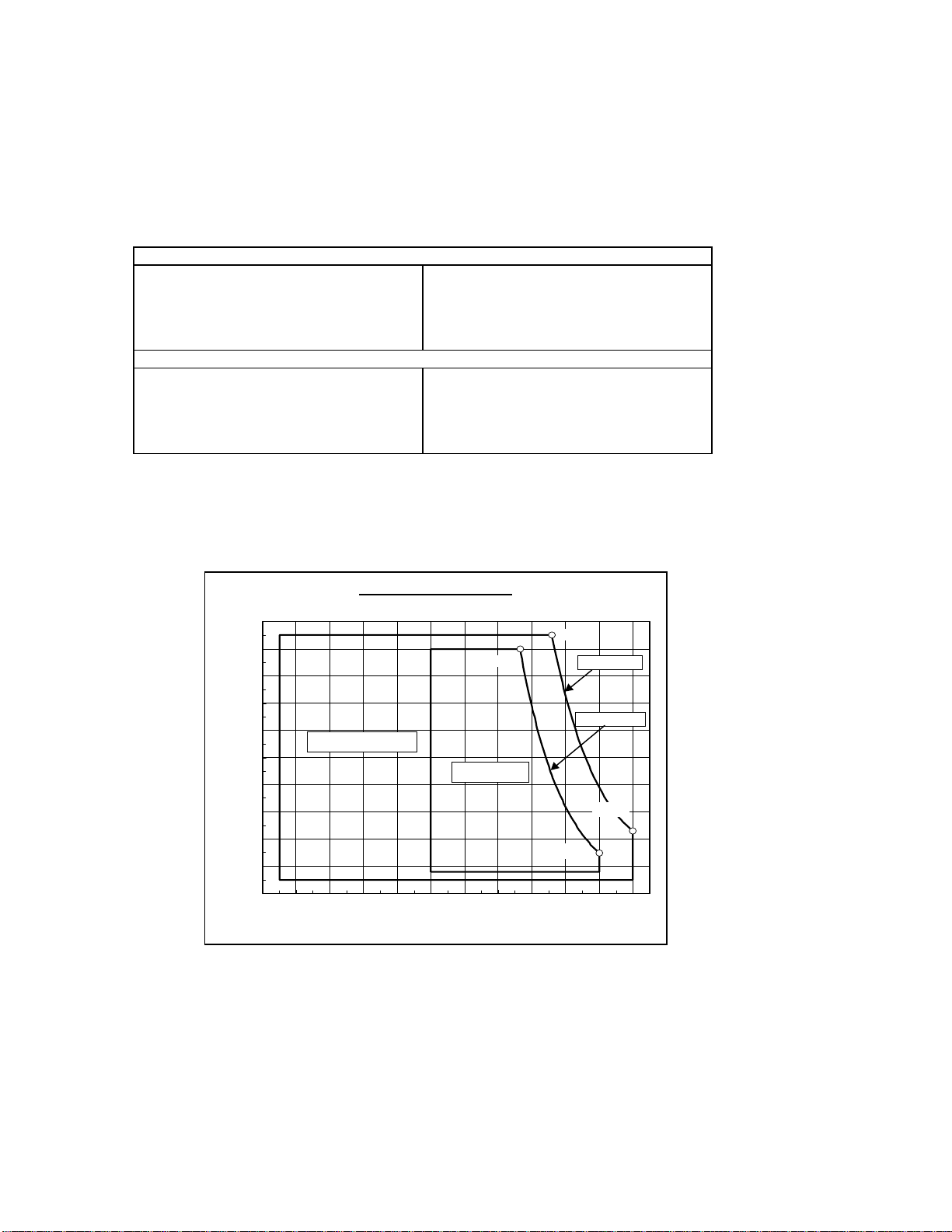
6.1 Environment
6.1.1 Temperature and humidity
Operating conditions
Temperature
Relative humidity
Maximum wet bulb temperature
Maximum temperature gradient
Altitude
Nonoperating conditions
Temperature
Relative humidity
Maximum wet bulb temperature
Maximum temperature gradient
Altitude
Table 12. Environmental condition
The system is responsible for providing sufficient air movement to maintain surface temperatures below
60°C at the center of top cover and below 63°C at the center of the drive circuit board assembly.
The maximum storage period in the shipping package is one year.
5 to 55°C (See note below)
8 to 90% nonconde nsing
29.4°C noncondensing
20°C/hour
–300 to 3048 m (10,000 ft)
–40 to 65°C
5 to 95% nonconde nsing
40°C noncon densing
20°C/hour
–300 to 12,192 m (40,000 ft)
Specification (Environment)
100
90
80
70
60
Non Operating
50
40
Relative Humidity (%)
30
20
10
0
-45 -35 -25 -15 -5 5 15 25 35 45 55 65
Temperature (degC)
Figure 1. Limits of temperature and humidity
6.1.2 Corrosion test
31'C/90%
Operating
41'C/95%
W etBulb 40'C
W etBulb29.4'C
65'C/23%
55'C/15%
The hard disk drive must be functional and show no signs of corrosion after being exposed to a
temperatur e h um idity stress of 50° C / 9 0%RH (relative humidity) for one week followed by a tempe r at ure
and humidity drop to 25'C/40%RH in 2 hours.
Page 24 of 171
Page 25

5K250 SATA OEM Specificat ion
6.1.3 Radiation noise
The disk drive shall work without degradation of the soft error rate under the following magnetic flux
density limits at the enclosure surface.
Frequency (KHz) Limits (uT RMS)
0–60 500
61–100 250
101–200 100
201–400 50
Table 13. Magnetic flux density limits
6.1.4 Conductive noise
The disk drive shall work without soft error degradation in the freque ncy range from DC to 20 Mhz
injected through any two of the mounting screw holes of the drive when an AC cu rrent of up to 45 mA
(p-p) is applied through a 50-ohm resistor connected to any two mounting screw holes.
The disk drive will withstand radiation and conductive noise within the limits shown below. The test
method is defined in the Noise Susceptibility Test Method specification, P/N 95F3944.
Page 25 of 171
Page 26

5K250 SATA OEM Specificat ion
6.2 DC power requirements
Connection to the product should be made in a safety extra low voltage (SELV) circuits. The voltage
specifications are applied at the power connector of the drive.
Item Requirements
Nominal supply +5 Volt dc
Supply voltage –0.3 Volt to 6.0 Volt
Power supply ripple (0–20
1
MHz)
Tolerance 2
Supply rise time 1–100 ms
Watts (RMS Typical)
Performanc e I dl e av erage 3
Active Idle average 0.8
Low Power Idle average 0.55
Read average 4
Write average 1.8
Seek average 5
Standby 0.2
Sleep 0.1
Startup (maximum peak) 6
Average from power on to
ready
Table 14. DC Power requirements
7
100 mV p-p max.
±5%
1.7
1.8
2.2
5.0
3.8
Footnotes:
1. The maximum fixed disk ripple is measured at the 5 volt input of the drive.
2. The disk drive shall not incur damage for an over voltage condition of +25% (maximum
3. The idle current is specified at an inner track.
4. The read/write current is specified based on three operations of 63 sector read/write per
5. The seek average current is specified based on three operations per 100 ms.
6. The worst case operating current includes motor surge.
7. “Typical” mean average of the drive population tested at nominal environmental and
duration of 20 ms) on the 5 volt nominal supply.
100 ms.
voltage condi t i o ns .
Page 26 of 171
Page 27

5K250 SATA OEM Specificat ion
6.2.1 Power consumption efficiency
Capacity 250GB 160GB 120GB 80GB
Power Consumption Efficiency (Watts/GB) 0.0022 0.0034 0.0046 0.0069
Table 15. Power consumption efficiency
Note: Power consumption efficiency is calculated as Power Consumption of Low Power Idle Watt/
Capacity (GB).
Page 27 of 171
Page 28

6.3 Reliability
6.3.1 Data reliability
5K250 SATA OEM Specificat ion
Probability of no t recovering data is 1 in 10
ECC implementation
On-the-fly correction performed as a part of read channel function recovers up to 16 symbols of error in 1
sector (1 symbol is 10 bits).
13
bits read
6.3.2 Failure prediction (S.M.A.R.T.)
The drive supports Self-monitoring, analysis and reporting technology (S.M.A.R.T.) function. The details
are described in section 11.8, "S.M.A.R.T. Function" on page 84 and in Section 13.32, "S.M.A.R.T.
Function Set (B0h)" on page 163.
6.3.3 Cable noise interference
To avoid any degradation of performance throughput or error when the interface cable is routed on top or
comes in contact with the HDA assembly, the drive must be grounded electrically to the system frame by
four screws. The common mode noise or voltage level difference between the system frame and power
cable ground or AT interface cable ground should be in the allowable level specified in the power
requirement section.
6.3.4 Service life and usage condition
The drive is designed to be used under the following conditions:
The drive should be operated within specifications of shock, vibration, temperature, humidity, altitude,
and magnetic fi el d .
The drive should be protected from ESD.
The breathing hole in the top cover of the drive should not be covered.
Force should not be applied to the cover of the drive.
The specified power requirements of the drive should be satisfied.
The drive frame should be grounded electrically to the system through four screws.
The drive should be mounted with the recommended screw depth and torque.
The interface physical and electrical requirements of the drive should satisfy Serial ATA Revis i on 2.6.
The power-off sequence of the drive should comply with the 6.3.6.2,"Required power-off
sequence.”
Service life of the drive is approximately 5 years or 20,000 power on hours, whichever comes first, under
the following assumptions:
Less than 333 power on hours per month.
Seeking/Writing/Reading operation is less than 20% of power on hours.
This does not represent any warranty or warranty period. Applicable warranty and warranty period are
covered by the purchase agreement.
Page 28 of 171
Page 29

5K250 SATA OEM Specificat ion
6.3.5 Preventive maintenance
None.
6.3.6 Load/unload
The product supports a minimum of 600,000 normal load/unloads.
Load/unload is a functional mechanism of the hard disk drive. It is controlled by the drive micro code.
Specifically, unloading of the heads is invoked by the following commands:
Standby
Standby immediate
Sleep
Load/unload is also invoked as one of the idle modes of the drive.
The specified start/stop life of the product assumes that load/unload is operated normally, not in
emergency mode.
6.3.6.1 Emergency unload
When hard disk drive power is interrupted while the heads are still loaded the micro code cannot operate
and the normal 5-volt power is unavailable to unload the heads. In this case, normal unload is not
possible. The heads are unloaded by routing the back EMF of the spinning motor to the voice coil. The
actuator velocity is greater than the normal case and the unload process is inherently less controllable
without a normal seek current profile.
Emergency unload is intended to be invoked in rare situations. Because this operation is inherently
uncontrolled, it is more mechanically stressful than a normal unload.
The drive supports a minimum of 20,000 emergency unloads.
6.3.6.2 Required Power-Off Sequence
The required host system sequence for removing power from the drive is as follows:
Step 1: Issue one of the following commands.
Standby
Standby immediate
Sleep
Note: Do not use the Flush Cache command for the power off sequence because this command
does not invoke Unload.
Step 2: Wait until the Command C omplete status is returned.
In a typical case 500 ms are required for the command to finish completion; however, the host system
time out value needs to be 30 seconds considering error recovery time.
Step 3: Terminate power to HDD.
This power-down sequence should be followed for entry into any system power-down state, system
suspend state, or system hibernation state. In a robustly designed system, emergency unload is limited
to rare scenarios, such as battery removal during operation.
6.3.6.3 Power switch design considerations
In systems that use the Travelstar 5K250 consideration should be given to the design of the system
power switch.
Hitachi recommends that the switch operate under control of the host system, as opposed to being
hardwired. The same recommendation is made for cover-close switches. When a hardwired switch is
turned off, emergency unload occurs, as well as the problems cited in section 5.1, "Data loss by power
off" and section 5.2, “Write Cache”.
Page 29 of 171
Page 30

5K250 SATA OEM Specificat ion
6.3.6.4 Test considerations
Start/stop testing is classically performed to verify head/disk durability. The heads do not land on the disk,
so this type of test should be viewed as a test of the load/unload function.
Start/Stop testing should be done by commands through the interface, not
Simple power cycling of the drive invokes the emergency unload mechanism and subjects the HDD to
nontypical mechanical stress.
Power cycling testing may be required to test the boot-up function of the system. In this case HItachi
recommends that the power -off portion of the cycle con tain the seque nce specified in section 6.3.6.2,
"Required Power-Off Sequence”. If this is not done, the emergency unload function is invoked and
nontypical stress results.
by power cycling the drive.
Page 30 of 171
Page 31

5K250 SATA OEM Specificat ion
6.4 Mechanical specifications
6.4.1 Physical dimensions and weight
The following figure lists the dimensions for the drive.
Model Height (mm) Width (mm) Length (mm) Weight (gram)
250GB, 160GB models 9.5±0.2 69.85±0.25 100.2±0.25 102 Max
120GB, 80GB models 9.5±0.2 69.85±0.25 100.2±0.25 95 Max
Table 16. Physical dimensions and weight
6.4.2 Mounting hole locations
The mounting hole locations and size of the drive are shown below.
Figure 2. Mounting hole locations
Page 31 of 171
Page 32

5K250 SATA OEM Specificat ion
6.4.3 Connector description
Connector specifications are included in section 7.2, "Interface connector" .
6.4.4 Mounting orientation
The drive will operate in all axes (six directions) and will stay within the specified error rates when tilted ±5
degrees from these positions.
Performance and error rate will stay within specification limits if the drive is operated in the other
permissible orientations from which it was formatted. Thus a drive formatted in a horizontal orientation will
be able to run vertically and vice versa.
The recommended mounting screw torque is 0.3±0.05 Nm.
The recommended mounting screw depth is 3.0±0.3 mm for bottom and 3.5±0.5 mm for horizontal
mounting.
The user is responsible for using the appropriate screws or equivalent mounting hardware to mount
the drive securely enough to prevent excessive motion or vibration of the drive at seek operation or
spindle rotation.
6.4.5 Load/unload mechanism
The head load/unload mechanism is provided to protect the disk data during shipping, movement, or
storage. Upon power down, a head unload mechanism secures the heads at the unload position. See
section 6.5.4, "Nonoperating shock" for additional details.
Page 32 of 171
Page 33

5K250 SATA OEM Specificat ion
6.5 Vibration and shock
All vibration and shock measurements in this section are for drives without mounting attachments for
systems. The input level shall be applied to the normal drive mounting points.
Vibration tests and shock tests are to be conducted by mount ing the drive to a table using the bottom four
mounting holes.
6.5.1 Operating vibration
The drive will operate without a hard error while being subjected to the following vibration levels.
6.5.1.1 Random vibration
The test consists of 30 minutes of random vibration using the power spectral density (PSD) levels below.
The vibration test level is 6.57 m/s e c
Random vibration PSD profile Breakpoint
Hz m x 10n (m2/sec4)/Hz
5 1.9 x E–3
17 1.1 x E–1
45 1.1 x E–1
48 7.7 x E–1
62 7.7 x E–1
65 9.6 x E–1
150 9.6 x E–1
200 4.8 x E–2
500 4.8 x E–2
Table 17. Random vibration PSD profile breakpoints (operating)
2
RMS (Root Mean Square) (0.67 G RMS).
6.5.1.2 Swept sine vibration
Swept sine vibration (zero to peak 5 to
500 to 5 Hz sine wave )
9.8 m/sec2 (1 G) (5-500 Hz) 1.0
Table 18. Swept sine vibration
Sweep rate (oct/min)
Page 33 of 171
Page 34

5K250 SATA OEM Specificat ion
6.5.2 Nonoperating vibration
The disk drive withstands the following vibration levels without any loss or permanent damage.
6.5.2.1 Random vibration
The test consists of a random vibration applied in each of three mutually perpendicular axes for a duration
of 15 minutes per axis. The PSD levels for the test simulating the shipping and relocation environment is
shown below.
Hz (m/sec
2.5 0.096
5 2.88
40 1.73
500 1.73
2
)/Hz
Table 19. Random Vibration PSD Profile Breakpoints (nonoperating)
Note: Overall RMS level of vibration is 29.50 m/sec2 (3.01 G).
6.5.2.2 Swept sine vibration
49 m/sec2 (5 G) (zero-to-peak), 10 to 500 to 10 Hz sine wave
0.5 oct/min sweep rate
25.4 mm (peak-to-peak) displacement, 5 to 10 to 5 Hz
6.5.3 Operating shock
The hard disk drive meets the criteria in the table below while operating under these conditions:
The shock test consists of 10 shock inputs in each axis and direction for a total of 60.
There must be a minimum delay of 3 seconds between shock pulses.
The disk drive will operate without a hard error while subjected to the following half-sine shock pulse.
Duration of 1 ms Duration of 2 ms
1960 m/sec2 (200 G) 3920 m/sec2 (400 G)
Table 20. Operating shock
The input level shall be applied to the normal disk driv e subsystem moun ting points u sed to secure the
drive in a normal system.
6.5.4 Nonoperating shock
The drive withstands the following half-sine shock pulse without any data loss or permanent damage.
Duration of 1 ms Duration of 11 ms
9800 m/sec2 (1000 G) 1470 m/sec2 (150 G)
Table 21. Nonoperating shock
The shocks are applied for each direction of the drive for three mutually perpendicular axes, one axis at a
time. Input levels are measured on a base plate where the drive is attached with four screws.
Page 34 of 171
Page 35

5K250 SATA OEM Specificat ion
6.6 Acoustics
6.6.1 Sound power level
The criteria of A-weighted sound power level are described below.
Measurements are to be taken in accordance with ISO 7779. The mean of the sample of 40 drives is to
be less than the typical value. Each drive is to be less than the maximum value. The drives are to meet
this requirement in both board down orientations.
A-weighted Sound Power Typical (Bels) Maximum (Bels)
Idle 2.4 2.7
Operating 2.6 2.9
Table 22. Weighted sound power
The background power levels of the acoustic test chamber for each octave band are to be recorded.
Sound power tests are to be conducted with the drive supported by spacers so that the lower surface of
the drive be located 25±3 mm above from the chamber floor. No sound absorbing material shall be used.
The acoustical characteristics of the disk drive are measured under the following conditions:
Mode definitions
Idle mode: Power on, disks spinning, track following, unit ready to receive and respond to control line
commands.
Operating mode: Continuous random cylinder selection and seek operation of the actuator with a
dwell time at each cylinder. The seek rate for the drive can be calculated as shown below.
Ns = 0.4/(Tt + T 1)
where:
Ns = average seek rate in seeks/s
Tt = published seek time from on e random track to another without including rotational
latency
T1= equivalent time in seconds for the drive to rotate by half a revolution
6.6.2 Discrete tone penalty
Discrete tone penalties are added to the A-weighted sound power (Lw) with the following formula only
when determining compliance.
Lwt(spec) = Lw = 0.1Pt + 0.3 < 4.0 (Bels)
where
Lw = A-weighted sound powe r level
Pt = Value of desecra t e t one penalty = dLt – 6.0(dB A )
dLt = Tone-to-noise ratio taken in accordance with ISO 7779 at each octave band.
Page 35 of 171
Page 36

5K250 SATA OEM Specificat ion
6.7 Identification labels
The following labels are affixed to every drive:
A label which is placed on the top of the head disk assembly containing the statement "Made by
Hitachi" or equivalent, part number, EC number, and FRU number.
A bar code label which is placed on the disk drive based on user request. The location on the disk
drive is to be designated in the drawing provided by the user.
Labels containin g t he vendor's name, di sk drive model numb e r , s e ri a l number, place of m a nufacture,
and UL/CSA logos.
The presence of labels containing jumper information depends on the customer.
6.8 Electromagnetic compatibility
When installed in a suitable enclosure and exercised with a random accessing routine at maximum data
rate, the drive meets the following worldwide electromagnetic compatibility (EMC) requirements:
United States Federal Communications Commission (FCC) Rules and Regulations (Class B),
Part 15. RFI Suppression German National Requirements
RFI Japan VCCI, Requirements of HITACHI products
EU EMC Directive, Technical Requirements and Conformity Assessment Procedures
6.8.1 CE Mark
The product is certified for compliance with EC directive 89/336/EEC. The EC marking for the certification
appears on the drive.
6.8.2 C-Tick Mark
The product complies with the Australian EMC standard "Limits and methods of measurement of radio
disturbance characteristics of information technology equipment, AS/NZS 3548:1995 Class B."
6.8.3 BSMI Mark
The product complies with the Taiwan EMC standard “Limits and methods of measurement of radio
disturbance characteristics of information technology equipment, CNS 13438 (C6357)”
6.8.4 MIC Mark
The product complies with the Korea EMC standard. The regulation for certification of information and
communication equipment is based on “Telecommunications Basic Act” and “Radio Waves Act” Korea
EMC requirment are based technically on CISPR22:1993-12 measurement standards and limits. MIC
standards are likewise based on IEC standards.
Page 36 of 171
Page 37

5K250 SATA OEM Specificat ion
6.9 Safety
6.9.1 UL and CSA approval
All models of the Travelstar 5K250 are qualified per UL60950-1:2003
6.9.2 IEC compliance
All models of the Travelstar 5K250 comply with IEC 60950-1:2001.
6.9.3 German Safety Mark
All models of the Travelstar 5K250 are approved by TUV on Test Requirement: EN 60950-1:2001, but the
GS mark has not been obtained.
6.9.4 Flammability
The printed circuit boards used in this product are made of material with a UL recognized
flammability rating of V-1 or better. The flammability rating is marked or etched on the board. All
other parts not considered electrical components are made of material with a UL recognized
flammability rating of V-1 or better except minor mechanical parts.
6.9.5 Secondary circuit protection
This product utilizes printed circuit wiring that must be protected against the possibility of
sustained combustion due to circuit or component failures as defined in C-B 2-4700-034 (Protection
Against Combustion). Adequate secondary over current protection is the responsibility of the using
system.
The user must protect the drive from its electrical short circuit problem. A 10 amp limit is required
for safety purpose.
6.10 Packaging
Drives are packed in ESD protective bags and shipped in appropriate containers.
6.11 Substance restriction requirements
The product complies with the Directive 2002/95/EC of the European Parliament on the restrictions
of the use of the certain hazardous substances in electrical and electronic equipment (RoHS).
Page 37 of 171
Page 38

5K250 SATA OEM Specificat ion
7 Electrical interface specifications
7.1 Cabling
The maximum cable length from the host system to the hard disk drive plus circuit pattern length in the
host system shall not exceed 1 meter.
7.2 Interface connector
The figure below shows the physical pin location.
Figure 3. Interface connector pin assignments
All pins are in a single row, with a 127 mm(.050”) pitch.
The comments on the mating sequence in Table in the section 7.3 apply to the case of back-plane
blind-mate connector only. In this case, the mating sequences are:(1)the ground pins P4 and P12;(2)
the pre-charge power pins and the other ground pins; and (3) the signal pins and the rest of the
power pins.
There are three power pins for each voltage. One pin from each voltage is used for pre-charge in the
backplane blind-mate situation.
If a device uses 3.3V, then all V33 pins must be terminated. Otherwise, it is optional to terminate any
of the V33 pins
If a device uses 5.0V, then all V5 pins must be terminated. Otherwise, it is optional to terminate any
of the V5 pins
If a device uses 12.0V, then all V12 pins must be terminated. Otherwise, it is optional to terminate
any of the V12 pins.
Page 38 of 171
Page 39

7.3 Signal definitions
The pin assignments of interface signals are listed as follows:
5K250 SATA OEM Specificat ion
Signal S4 Gnd 2nd mate Gnd
No.
S1 GND 2nd mate Gnd
S2 A+ Differential signal A from Phy RX+ Input
S3 A-
S5 B- Differential signal B from Phy TX- Output
S6 B+
S7 Gnd 2nd mate Gnd
Power P9 V5 5V power 5V
Table 23. Interface connector pins and I/O signals
P1 V33 3.3V power 3.3V
P2 V33 3.3V power 3.3V
P3 V33 3.3V power, pre-charge, 2nd Mate 3.3V
P4 Gnd 1st mate Gnd
P5 Gnd 2nd mate Gnd
P6 Gnd 2nd mate Gnd
P7 V5 5V power,pre-charge,2nd Mate 5V
P8 V5 5V power 5V
P10 Gnd 2nd mate Gnd
DAS/DSS
P11
P12 Gnd 1st mate Gnd
P13 V12 12V power,pre-chage,2nd mate V12
P14 V12 12V power V12
P15 V12 12V power V12
Plug Connector pin definition Signal I/O
RX- Input
TX+ Output
Key and spacing separate signal and power
segments
Device Activity Signal / Disable Staggered
Spinup
1
Note 1
Note 1;
Pin P11 is used by the drive to provide the host with an activity indication a nd by the host to
indicate whether staggered spinup should be used.
The signal the drive provides for activity indication is a low-voltage low-current driver.
If pin P11 is asserted low the drive shall disable staggered spin-up and immedia tely initiate
spin-up. If pin P11 is not connected in the host (floating), the drive shall enable staggered spin-up.
7.3.1 TX+ / TX-
These signal are the outbound high-speed differential signals that are connected to the serial ATA
cable
7.3.2 RX+ / RX-
These signals are the inbound high-speed differential signals that are connected to the serial ATA
cable.
The following standard shall be referenced about signal specifications.
Serial ATA: High Speed Serialized AT Attachment Revision 1.0a 7-January -2003
Page 39 of 171
Page 40

5K250 SATA OEM Specificat ion
7.3.3 Out of band signaling
Figure 4 shows the timing of COMRESET, COMINIT and COMWAKE.
COMRESET/COMINIT
t1
t2
COMWAKE
PARAMETER
T1 ALINE primitives 106.7
T2 Spacing 320
T3 ALIGN primitives 106.7
T4 Psacing 106.7
Figure 4. Parameter descriptions
t3
DESCRIPTION
t4
Nominal (ns)
Page 40 of 171
Page 41

Part 2 Interface Specification
5K250 SATA OEM Specificat ion
Page 41 of 171
Page 42

5K250 (SATA) OEM Specification
8 General
8.1 Introduction
The host interface of HTS5425XXK9SA00 / HTS5425XXK9A300 will be described in part2.
The interface conforms to following Working Document of Information technology with certain
limitations described in the chapter 9 “Deviations from Standard”
Serial ATA International Organization : Serial ATA Revision 2.6 dated on 15 February 2007
AT Attachment 8 – ATA/ATAPI Command Set (ATA8-ACS) Revision 3f dated on 11 December 2006
HTS5425XXK9SA00 / HTS5425XXK9A300 support following functions as Vendor Specific Function.
• Format Unit Function
• SENSE CONDITION command
8.2 Terminology
Device
Host
INTRQ
Device indicates HTS5425XXK9SA00 / HTS5425XXK9A300
Host indicates the system that the device is attached to.
Interrupt request (Device or Host)
Page 42 of 171
Page 43

5K250 (SATA) OEM Specification
9 Deviations from Standard
The device conforms to the referenced specifications, with deviations described below.
The interface conforms to the Working Document of Information Technology, AT Attachment 8 –
ATA/ATAPI Command Set (ATA/ATAPI8-ACS) Revision 3f dated 11 Dec. 2006, with deviation as
follows:
S.M.A.R.T. Return Status
Check Power Mode
S.M.A.R.T. RETURN STATUS subcommand does not chec k advisory at tribu tes.
That is, the device will not report threshold exceeded condition unless pre-fa ilure
attributes exceed their corresponding thresh ol ds. For example, Powe r-On Hours
Attribute never results in negative reliability status.
Check Power Mode command returns FFh to S ector Count Register when the device
is in Idle mode. This command does not support 80h as the return value.
10 Physical Interface
Physical Interface is described in Functional Specification part.
11 Registers
In Serial ATA, the host adapter contains a set of registers that shadow the contents of the traditional
device registers, referred to as the Shadow Register Block. Shadow Register Block registers are
interface registers used for delivering commands to the device or posting status from the device.
About details, please refer to the Serial ATA Specification.
In the following cases, the host adapter sets the BSY bit in its shadow Status Register and transmits
a FIS to the device containing the new contents.
• Command register is written in the Shadow Register Block
• Device Control register is written in the Shadow Register Block with a change of state of the
SRST bit
• COMRESET is requested
Page 43 of 171
Page 44

5K250 (SATA) OEM Specification
11.1 Register naming convention
This specification uses the same naming conventions for the Command Block Registers as the
ATA8-ACS standard. However, the register naming convention is different from that uses in the
Serial ATA 2.6 specification. The following table defines the corresponding of the register names
used in this specification with those used in the Serial ATA 2.6 specification.
Register name in this
Serial ATA register name
Features Feature current
Features (exp) Feature previous
Sector count Sector count current Sector count HOB=0
Sector count (exp) Sector count previous Sector count HOB=1
LBA low LBA low current LBA low HOB=0
LBA low (exp) LBA low previous LBA low HOB=1
LBA mid LBA mid current LBA mid HOB=0
LBA mid (exp) LBA mid previous LBA mid HOB=1
LBA high LBA high current LBA mid HOB=0
LBA high (exp) LBA high previous LBA mid HOB=1
Device Device Device
Command Command N/A
specification when writing
registers
Register name in this
specification when reading
registers
Control Device Control N/A
Status N/A Status
Error N/A Error
Table 24 Register naming convention and correspondence
11.2 Command register
This register contains the command code being sent to the device. Command execution begins
immediately after this register is written. The command set is shown in “Table 40 Command set”.
All other registers required for the command must be set up before writing the Command Register.
11.3 Device Control Register
Device Control Register
7 6 5 4 3 2 1 0
- - - - 1 SRST -IEN 0
Table 25 Device Control Register
Bit Definitions
SRST (RST)
Software Reset. The device is held reset when RST=1. Setting RST=0 reenables the device.
Page 44 of 171
Page 45

5K250 (SATA) OEM Specification
The host must set RST=1 and wait for at least 5 m icroseconds before setting RST=0, to
ensure that the device recognizes the reset.
-IEN
Interrupt Enable. When IEN=0, and the device is selected, device interrupts to the host will
be enabled. When IEN=1, or the device is not selected, device interrupts to the host will be
disabled.
11.4 Device Register
Device Register
7 6 5 4 3 2 1 0
- L - 0 HS3 HS2 HS1 HS0
Table 26 Device Register
This register contains the device and head numbers.
Bit Definitions
L
HS3,HS2,HS1,HS0
Binary encoded address mode select. When L=0, addre ssi ng is by CHS mode. When L=1,
addressing is by LBA mode.
The HS3 through HS0 contain bits 24-27 of the LBA. At command completion, these bi ts are
updated to reflect the current LBA bits 24-27.
11.5 Error Register
Error Register
7 6 5 4 3 2 1 0
CRC UNC 0 IDNF 0 ABRT TK0NF AMNF
Table 27 Error Register
This register contains status from the last command executed by the device, or a diagnostic code.
At the completion of any command except Execute Device Diagnostic, the contents of this register
are valid always even if ERR=0 in the Status Register.
Following a power on, a reset, or completion of an Execute Device Diagnostic command, this register
contains a diagnostic code. See “Table 31 Diagnostic Codes” for the definition.
Bit Definitions
ICRCE (CRC)
UNC
IDNF (IDN)
ABRT (ABT)
TK0NF (T0N)
AMNF (AMN)
Interface CRC Error. CRC=1 indicates a CRC error has occurred on the data bus during a
Ultra-DMA transfer.
Uncorrectable Data Error. UNC=1 indicates an uncorrectable data error has been
encountered.
ID Not Found. IDN=1 indicates the requested sector’s ID field could not be found.
Aborted Command. ABT=1 indicates the requested command has been aborted due to a
device status error or an invalid parameter in an output register.
Track 0 Not Found. T0N=1 indicates track 0 was not found during a Recalibrate comma nd.
Address Mark Not Found. AMN=1 indicates the data address mark has not been found after
finding the correct ID field for the requested sector.
This bit is obsolete.
11.6 Features Register
This register is command specific. This is used with the Set Features command, S.M.A.R.T. Function
Set command and Format Unit command.
11.7 LBA High Register
This register contains Bits 16-23. At the end of the command, this register is updated to reflect the
current LBA Bits 16-23.
Page 45 of 171
Page 46

5K250 (SATA) OEM Specification
When 48-bit addressing commands are used, the “most recently written” content contains LBA Bits
16-23, and the “previous content” contains Bits 40-47. The 48-bit Address feature set is described in
“12.14 48-bit Address Feature Set”.
11.8 LBA Low Register
This register contains Bits 0-7. At the end of the command, this register is updated to reflect the
current LBA Bits 0-7.
When 48-bit commands are used, the “most recently written” content contains LBA Bits 0-7, and the
“previous content” contains Bits 24-31.
11.9 LBA Mid Register
This register contains Bits 8-15. At the end of the command, this register is updated to reflect the
current LBA Bits 8-15.
When 48-bit addressing commands are used, the “most recently written” content contains LBA Bits
8-15, and the “previous content” contains Bits 32-39.
11.10 Sector Count Register
This register contains the number of sectors of data requested to be transferred on a read or write
operation between the host and the device. If the value in the register is set to 0, a count of 256
sectors (in 28-bit addressing) or 65,536 sectors (in 48-bit addressing) is specified.
If the register is zero at command completion, the command was successful. If not successfully
completed, the register contains the number of sectors which need to be transferred in order to
complete the request.
The contents of the register are defined otherwise on some commands. These definitions are given in
the command descriptions.
11.11 Status Register
Status Register
7 6 5 4 3 2 1 0
BSY DRDY DF DSC DRQ CORR IDX ERR
Table 28 Status Register
This register contains the device status. The contents of this register are updated whenever an error
occurs and at the completion of each command.
If the host reads this register when an interrupt is pending, it is considered to be the interrupt
acknowledge. Any pending interrupt is cleared whenever this register is read.
If BSY=1, no other bits in the register are valid.
Bit Definitions
BSY
DRDY (RDY)
DF
DSC
Busy. BSY=1 whenever the device is accessing the registers. The host should not read or
write any registers when BSY=1. If the host reads any register w hen BS Y=1, the contents of
the Status Register will be returned.
Device Ready. RDY=1 indicates that the de vice is capable of responding to a command.
RDY will be set to 0 during power on until the device is ready to accept a command.
Device Fault. DF=1 indicates that the de vice has detected a write faul t condition. DF is set to
0 after the Status Register is read by the host.
Device Seek Complete. DSC=1 indicate s that a seek has completed and the device head is
Page 46 of 171
Page 47

DRQ
CORR (COR)
IDX
ERR
5K250 (SATA) OEM Specification
settled over a track. DSC is set to 0 by the device just before a seek begins. When an error
occurs, this bit is not changed until the Status Register is read by the host, at which time the
bit again indicates the current seek complete status.
When the device enters into or is in Standby mode or Sleep mode, this bit is set by device in
spite of not spinning up.
Data Request. DRQ=1 indicates tha t the device is ready to transfer a word or byte of data
between the host and the device. The host should not write the Command register w hen
DRQ=1.
Corrected Data. Always 0.
Index. Always 0
ERR=1 indicates that an error occurred during execution of the previous command. The
Error Register should be read to determine the error type. The device sets ERR=0 when the
next command is received from the host.
Page 47 of 171
Page 48

5K250 (SATA) OEM Specification
12 General Operation Descriptions
12.1 Reset Response
There are three types of reset in ATA as follows:
Power On Reset (POR)
COMRESET
Soft Reset (Software Reset)
The actions of each reset are shown in “Table 29 Reset Response Table”
POR COMRESET Soft Reset
Aborting Host interface - o o
Aborting Device operation - (*1) (*1)
Initialization of hardware O x x
Internal diagnostic O x x
Starting spindle motor (*5) x x
Initialization of registers (*2) O o o
Reverting programmed parameters to default O (*6) (*3)
- Number of CHS (set by Initialize Device Parameter)
- Multiple mode
- Write cache
- Read look-ahead
- ECC bytes
- Volatile max address
Power mode (*5) (*4) (*4)
Reset Standby timer value o o x
O ---- execute
X ---- not execute
Note.
(*1) Execute after the data in write cache has been written.
(*2) Default value on POR is shown in “Table 30 Default Register Values” on Page 49.
(*3) The Set Features command with Feature register = CCh enables the device to
revert these parameters to the power on defaults.
(*4) In the case of sleep mode, the device goes to standby mode. In other case,
the device does not change current mode.
(*5) According to the initial power mode selection.
(*6) See 12.15 Software Setting Preservation Feature Set.
Table 29 Reset Response Table
The device executes a series of electrical circuitry diagnostics, spins up the HDA,
tests speed and other mechanical parametric, and sets default values.
COMRESET is issued in Serial ATA bus.
The device resets the interface circuitry as well as Soft Reset.
SRST bit in the Device Control Register is set, then is reset.
The device resets the interface circuitry according to the Set Features requirement.
12.1.1 Register Initialization
After power on, COMRESET, or software reset, the register values are initialized as show n in the foll owi ng tab le.
Page 48 of 171
Page 49

5K250 (SATA) OEM Specification
Register Default Value
Error Diagnostic Code
Sector Count 01h
LBA Low 01h
LBA Mid 00h
LBA High 00h
Device 00h
Status 50h
Alternate Status 50h
Table 30 Default Register Values
The meaning of the Error Register diagnostic codes resulting from power on, COMRESET or the
Execute Device Diagnostic command are shown in the following table.
Code Description
01h No error Detected
02h Formatter device error
03h Sector buffer error
04h Ecc circuitry error
05h Controller microprocessor error
Table 31 Diagnostic Codes
12.2 Diagnostic and Reset considerations
The Set Max password, the Set Max security mode and the Set Max unlock counter don’t retain over
a Power On Reset but persist over a COMRESET or Soft Reset.
For each Reset and Execute Device Diagnostic, the Diagnostic is done as follows:
Execute Device Diagnostic
In all the above cases: Power on, COMRESET, Soft reset, and the EXECUTE DEVICE
DIAGNOSTIC command the Error register is shown in the following table.
Device 0 Passed Error Register
Yes 01h
No 0xh
Where x indicates the appropriate Diagnos tic Code for the Power on, COMRESET, Soft reset, or Device
Diagnostic error.
Table 32 Reset error register values
Page 49 of 171
Page 50

5K250 (SATA) OEM Specification
12.3 Power-off considerations
12.3.1 Load/Unload
Load/Unload is a functional mechanism of the HDD. It is controlled by the drive microcode.
Specifically, unloading of the heads is invoked by the commands:
Command Response
Standby UL -> Comp.
Standby immediate UL -> Comp.
Sleep UL -> Comp.
“UL” means “unload”.
“Comp” means “complete”.
Table 33 Device’s behavior by ATA commands
Load/unload is also invoked as one of the idle modes of the drive.
The specified start/stop life of the product assumes that load/unload is operated normally, NOT in
emergency mode.
12.3.2 Emergency unload
When HDD power is interrupted while the heads are still loaded, the microcode cannot operate and
the normal 5V power is unavailable to unload the heads. In this case, normal unload is not possible,
so the heads are unloaded by routing the back-EMF of the spinning motor to the voice coil. The
actuator velocity is greater than the normal case, and the unload process is inherently less
controllable without a normal seek current profile.
Emergency unload is intended to be invoked in rare situations. Because this operation is inherently
uncontrolled, it is more mechanically stressful than a normal unload.
A single emergency unload operation is more stressful than 100 normal unloads. Use of emergency
unload reduces the start/stop life of the HDD at a rate at least 100X faster than that of normal
unload, and may damage the HDD.
12.3.3 Required power-off sequence
Problems can occur on most HDDs when power is removed at an arbitrary time. Examples:
Data loss from the write buffer.
If the drive is writing a se ctor, a partially-written sector with an incorrect ECC block results. The sector
contents are destroyed and reading that sector results in a hard error.
Heads possibly land in the data zone instead of landing zone, depending on the de sign of the HDD.
You may then turn off the HDD in the following order:
1. Issue Standby Immediate or sleep command.
2. Wait until COMMAND COMPLETE STATUS is returned. (It may take up to 350 ms in typical case)
3. Terminate power to HDD.
This power-down sequence should be followed for entry into any system power-down state, or system
suspend state, or system hibernation state. In a robustly designed system, emergency unload is
limited to rare scenarios such as battery removal during operation.
Page 50 of 171
Page 51

5K250 (SATA) OEM Specification
12.4 Sector Addressing Mode
All addressing of data sectors recorded on the device’s media is by a logical sector address. The
logical CHS address for HTS5425XXK9SA00 / HTS5425XXK9A300 is different from the actual
physical CHS location of the data sector on the disk media.
HTS5425XXK9SA00 / HTS5425XXK9A300 support both Logical CHS Addressing Mode and LBA
Addressing Mode as the sector addressing mode.
The host system may select either the currently selected CHS translation addressing or LBA
addressing on a command-by-command basis by using the L bit in the DEVICE register. So a host
system must set the L bit to 1 if the host uses LBA Addressing mode.
12.4.1 Logical CHS Addressing Mode
The logical CHS addressing is made up of three fields: the cylinder number, the head number and
the sector number. Sectors are numbered from 1 to the maximum value allowed by the current CHS
translation mode but can not exceed 255(0FFh). Heads are numbered from 0 to the maximum value
allowed by the current CHS translation mode but can not exceed 15(0Fh). Cylinders are numbered
from 0 to the maximum value allowed by the current CHS translation mode but cannot exceed
65535(0FFFFh).
When the host selects a CHS translation mode using the INITIALIZE DEVICE PARAMETERS
command, the host requests the number of sectors per logical track and the number of heads per
logical cylinder. The device then computes the number of logical cylinders available in requested
mode.
The default CHS translation mode is described in the Identify Device Information. The current CHS
translation mode also is described in the Identify Device Information.
12.4.2 LBA Addressing Mode
Logical sectors on the device shall be linearly mapped with the first LBA addressed sector (sector 0)
being the same sector as the first logical CHS addressed sector ( cylinder 0, head 0, sector 1).
Irrespective of the logical CHS translation mode currently in effect, the LBA address of a given
logical sector does not change. The following is always true:
LBA = ( (cylinder * heads_per_cylinder + heads)
* sectors_per_track ) + sector - 1
where heads_per_cylinder and sectors_per_tr ack ar e the current translat ion mode values.
On LBA addressing mode, the LBA value is set to the following register.
Device <--- LBA bits 27-24
LBA High <--- LBA bits 23-16
LBA Mid <--- LBA bits 15- 8
LBA Low <--- LBA bits 7- 0
12.5 Power Management Feature
The power management feature set permits a host to modify the behavior in a manner which
reduces the power required to operate. The power management feature set provides a set of
commands and a timer that enables a device to implement low power consumption modes.
HTS5425XXK9SA00 / HTS5425XXK9A300 implement the following set of functions.
1. A Standby timer
2. Idle command
3. Idle Immediate command
4. Sleep command
5. Standby command
6. Standby Immediate command
Page 51 of 171
Page 52

12.5.1 Power Mode
5K250 (SATA) OEM Specification
Sleep Mode
Standby Mode
Idle Mode
Active Mode
The lowest power consumption when the device is powered on occurs in Sleep Mode.
When in sleep mode, the device requires a reset to be activated.
The device interface is capable of acc epting commands, but as the media may not
immediately accessible, there is a delay whi le waiting for the spindle to reach
operating speed.
Refer to the section of Adaptive Battery L ife Extender Feature.
The device is in execution of a command or accessing the disk media with read
look-ahead function or write cache function.
12.5.2 Power Management Commands
The Check Power Mode command allows a host to determine if a device is currently in, going to or
leaving standby mode.
The Idle and Idle Immediate commands move a device to idle mode immediately from the active or
standby modes. The idle command also sets the standby timer count and starts the standby timer.
The sleep command moves a device to sleep mode. The device’s interface becomes inactive at the
completion of the sleep command. A reset is required to move a device out of sleep mode. When a
device exits sleep mode it will enter standby mode.
The Standby and Standby Immediate commands move a device to standby mode immediately from
the active or idle modes. The standby command also sets the standby timer count.
12.5.3 Standby/Sleep command completion timing
1. Confirm the completion of writing cached data in the buffer to media
2. Unload heads on the ramp
3. Set DRDY bit and DSC bit in Status Register
4. Activate the spindle break to stop the spindle motor
5. Wait until spindle motor is stopped
6. Perform post process
12.5.4 Status
In the active, idle and standby modes, the device shall have RDY bit of the status register set. If BSY
bit is not set, device shall be ready to accept any command.
In sleep mode, the device’s interface is not active. A host shall not attempt to read the device’s status
or issue commands to the device.
12.5.5 Interface Capability for Power Modes
Each power mode affects the physical interface as defined in the following table:
Mode BSY RDY Interface active Media
Active x x Yes Active
Idle 0 1 Yes Active
Standby 0 1 Yes Inactive
Sleep x x No Inactive
Table 34 Power conditions
Ready(RDY) is not a power condition. A device may post ready at the interface even though the
media may not be accessible.
Page 52 of 171
Page 53

5K250 (SATA) OEM Specification
12.5.6 Initial Power Mode at Power On
After power on the device goes to IDLE mode or STANDBY mode depending on the setting of the
Power Up in Standby Feature set
12.6 Advanced Power Management (Adaptive
Battery Life Extender 3) Feature
This feature provides power saving without performance degradation. The Adaptive Battery Life
Extender 3 (ABLE-3) technology intelligently manages transition among power modes within the
device by monitoring access patterns of the host.
This technology has three idle modes; Performance Idle mode, Active Idle mode, and Low Power Idle
mode.
This feature allows the host to select an advanced power management level. The advanced power
management level is a scale from the lowest power consumption setting of 01h to the maximum
performance level of FEh. Device performance may increase with increasing advanced power
management levels. Device power consumption may increase with increasing advanced power
management levels. The advanced power management levels contain discrete bands, described in the
section of Set Feature command in detail.
This feature set uses the following functions:
A SET FEATURES subcommand to enable Advanced Power Management
A SET FEATURES subcommand to disable Advanced Power Management
The Advanced Power Management feature is independent of the Standby timer setting. If both
Advanced Power Management level and the Standby timer are set, the device will go to the Standby
state when the timer times out or the device’s Advanced Power Management algorithm indicates
that it is time to enter the Standby state.
The IDENTIFY DEVICE response word 83, bit 3 indicates that Advanced Power Management
feature is supported if set. Word 86, bit 3 indicates that Advanced Power Management is enabled if
set.
Word 91, bits 7-0 contain the current Advanced Power Management level if Advanced Power
Management is enabled.
12.6.1 Performance Idle mode
This mode is usually entered immediately after Active mode command processing is complete,
instead of conventional idle mode. In Performance Idle mode, all electronic components remain
powered and full frequency servo remains operational. This provides instantaneous response to the
next command. The duration of this mode is intelligently managed as described below.
12.6.2 Active Idle mode
In this mode, power consumption is 45-55% less than that of Performance Idle mode. Additional
electronics are powered off, and the head is parked near the mid-diameter of the disk without
servoing. Recovery time to Active mode is about 20ms.
12.6.3 Low Power Idle mode
Power consumption is 60%-65% less than that of Performance Idle mode. The heads are unloaded on
the ramp, however the spindle is still rotated at the full speed. Recovery time to Active mode is about
300ms.
Page 53 of 171
Page 54

5K250 (SATA) OEM Specification
12.6.4 Transition Time
The transition time is dynamically managed by users recent access pattern, instead of fixed times.
The ABLE-3 algorithm monitors the interval between commands instead of the command frequency
of ABLE-2. The algorithm supposes that next command will come with the same command interval
distribution as the previous access pattern. The algorithm calculates the expected average saving
energy and response delay for next command in several transition time case based on this
assumption. And it selects the most effective transition time with the condition that the calculated
response delay is shorter than the value calculated from the specified level by Set Feature Enable
Advanced Power Management command.
The optimal time to enter Active Idle mode is variable depending on the users recent behavior. It is
not possible to achieve the same level of Power savings with a fixed entry time into Active Idle
because every users data and access pattern is different. The optimum entry time changes over time.
The same algorithm works for entering into Low Power Idle mode and Standby mode, which
consumes less power but need more recovery time switching from this mode to Active mode.
12.7 Interface Power Management Mode
(Slumber and Partial)
Interface Power Management Mode is supported by both Device-initiated interface power
management and Host-initiated interface power management. Please refer to the Serial ATA
Specification about Power Management Mode.
12.8 S.M.A.R.T. Function
The intent of Self-monitoring, analysis and reporting technology (S.M.A.R.T) is to protect user data
and prevent unscheduled system downtime that may be caused by predictable degradation and/or
fault of the device. By monitoring and storing critical performance and calibration parameters,
S.M.A.R.T devices employ sophisticated data analysis algorithms to predict the likelihood of
near-term degradation or fault condition. By alerting the host system of a negative reliability status
condition, the host system can warn the user of the impending risk of a data loss and advise the user
of appropriate action.
Since S.M.A.R.T. utilizes the internal device microprocessor and other device resources, there may
be some small overhead associated with its operation. However, special care has been taken in the
design of the S.M.A.R.T. algorithms to minimize the impact to host system performance. Actual
impact of S.M.A.R.T. overhead is dependent on the specific device design and the usage patterns of
the host system. To further ensure minimal impact to the user, S.M.A.R.T. capable devices are
shipped from the device manufacturer’s factory with the S.M.A.R.T. feature disabled. S.M.A.R.T.
capable devices can be enabled by the system OEMs at time of system integration or in the field by
aftermarket products.
12.8.1 Attributes
Attributes are the specific performance or calibration parameters that are used in analyzing the
status of the device. Attributes are selected by the device manufacturer based on that attribute’s
ability to contribute to the prediction of degrading or faulty conditions for that particular device. The
specific set of attributes being used and the identity of these attributes is vendor specific and
proprietary.
12.8.2 Attribute values
Attribute values are used to represent the relative reliability of individual performance or
calibration attributes. Higher attribute values indicate that the analysis algorithms being used by
Page 54 of 171
Page 55

5K250 (SATA) OEM Specification
the device are predicting a lower probability of a degrading or fault condition existing. Accordingly,
lower attribute values indicate that the analysis algorithms being used by the device are predicting a
higher probability of a degrading or fault condition existing. There is no implied linear reliability
relationship corresponding to the numerical relationship between different attribute values for any
particular attribute.
12.8.3 Attribute thresholds
Each attribute value has a corresponding attribute threshold limit which is used for direct
comparison to the attribute value to indicate the existence of a degrading or faulty condition. The
numerical value of the attribute thresholds are determined by the device manufacturer through
design and reliability testing and analysis. Each attribute threshold represents the lowest limit to
which its corresponding attribute value can be equal while still retaining a positive reliability status.
Attribute thresholds are set at the device manufacturer’s factory and cannot be changed in the field.
The valid range for attribute thresholds is from 1 through 253 decimal.
12.8.4 Threshold exceeded condition
If one or more attribute values are less than or equal to their corresponding attribute thresholds,
then the device reliability status is negative, indicating an impending degrading or faulty condition.
12.8.5 S.M.A.R.T. commands
The S.M.A.R.T. commands provide access to attribute values, attribute thresholds and other logging
and reporting information.
12.8.6 S.M.A.R.T operation with power management modes
The device saves attribute values automatically on every head unload timing except the emergency
unload, even if the attribute auto save feature is not enabled. The head unload is done not only by
Standby, Standby Immediate, or Sleep command, but also by the automatic power saving functions
like ABLE-3 or Standby timer. So basically it is not necessary for a host system to enable the
attribute auto save feature, when it utilizes the power management. If the attribute auto save
feature is enabled, attribute values will be saved after 30minutes passed since the last saving,
besides above condition.
12.9 Security Mode Feature Set
Security Mode Feature Set is a powerful security feature. With a device lock password, a user can
prevent unauthorized access to hard disk device even if the device is removed from the computer.
New commands are supported for this feature as below.
Security Set Password
Security Unlock
Security Erase Prepare
Security Erase Unit
Security Freeze Lock
Security Disable Password
12.9.1 Security mode
(‘F1’h)
(‘F2’h)
(‘F3’h)
(‘F4’h)
(‘F5’h)
(‘F6’h)
Following security modes are provided.
Device Locked mode
Device Unlocked mode
The device disables media access commands after power on. Media access
commands are enabled by either a security unlock command or a security
erase unit command.
The device enables all commands. If a password is not set this mode is
Page 55 of 171
Page 56

5K250 (SATA) OEM Specification
entered after power on, otherwise it is entered by a security unlock or a
security erase unit command.
Device Frozen mode
The device enables all commands except those which can update the devic e
lock function, set/change password. The device enters this mode via a
Security Freeze Lock command. It cannot quit this mode until power off.
12.9.2 Security Level
Following security levels are provided.
High level security
Maximum level security
When the device lock function is enabled and the User Password is
forgotten the device can be unlocked via a Master Password.
When the device lock function is enabled and the User Password is
forgotten then only the Master Password with a Security Erase Unit
command can unlock the device. Then user data is erased.
12.9.3 Password
This function can have 2 types of passwords as described below.
Master Password
User Password
The system manufacturer/dealer who intends to enable the device lock function for the end users,
must set the master password even if only single level password protection is required. Otherwise, if
the User Password is forgotten then no one can unlock the device which is locked with the User
Password.
When the Master Password is set, the device does NOT enable the Device
Lock Function, and the device can NOT be locked with the Master
Password, but the Master Password can be used for unlocking the device
locked.
The User Password should be given or changed by a system user. When the
User Password is set, the device enables the Device Lock Function, and
then the device is locked on next power on reset. If Software Setting
Preservation is disabled, the device is locked on COMRESET as well.
12.9.4 Master Password Revision Code
This Master Password Revision Code is set by Security Set Password command with the master
password. And this revision code field is returned in the Identify Device command word 92. The valid
revision codes are 0001h to FFFEh. The default value of Master Password Revision Code is FFFEh.
Value 0000h and FFFFh is reserved.
12.9.5 Operation example
12.9.5.1 Master Password setting
The system manufacturer/dealer can set a initial Master Password using the Security Set Password
command, without enabling the Device Lock Function.
12.9.5.2 User Password setting
When a User Password is set, the device will automatically enter lock mode the next time the device
is powered on.
Page 56 of 171
Page 57

5K250 (SATA) OEM Specification
Figure 5 Initial Setting
12.9.1.2 Operation from POR after User Password is set
When Device Lock Function is enabled, the device rejects media access command until a Security
Unlock command is successfully completed.
Page 57 of 171
Page 58

5K250 (SATA) OEM Specification
(*1) refer to Table 35 Command table for device lock operation on Page 60 and Table 36 Command table for
device lock operation - continued on Page 61.
Figure 6 Usual Operation
12.9.1.3 User Password Lost
If the User Password is forgotten and High level security is set, the system user can’t access any
data. However the device can be unlocked using the Master Password.
If a system user forgets the User Password and Maximum security level is set, data access is
impossible. However the device can be unlocked using the Security Erase Unit command to unlock
the device and erase all user data with the Master Password.
Page 58 of 171
Page 59

5K250 (SATA) OEM Specification
Figure 7 Password Lost
12.9.1.4 Attempt limit for SECURITY UNLOCK command
The SECURITY UNLOCK command has an attempt limit. The purpose of this attempt limit is to
prevent that someone attempts to unlock the drive by using various passwords many times.
The device counts the password mismatch. If the password does not match, the device counts it up
without distinguishing the Master password and the User password. If the count reaches 5, EXPIRE
bit(bit 4) of Word 128 in Identify Device information is set, and then SECURITY ERASE UNIT
command and SECURITY UNLOCK command are aborted until a power off. The count and EXPIRE
bit are cleared after a power on reset.
12.9.6 Command Table
This table shows the device’s response to commands when the Security Mode Feature Set (Device
lock function) is enabled.
Page 59 of 171
Page 60

5K250 (SATA) OEM Specification
Command Device
Locked
Mode
Device
Unlock
Mode
Device
Frozen
Mode
Check Power Mode o o o
Device Configuration RESTORE x o o
Device Configuration FREEZE LOCK o o o
Device Configuration IDENTIFY x o o
Device Configuration SET x o o
Execute Device Diagnostic o o o
Flush Cache x o o
Flush Cache Ext x o o
Format Track x o o
Format Unit x o o
Identify Device o o o
Idle o o o
Idle Immediate o o o
Idle Immediate with Unload option o o o
Initialize Device Parameters o o o
Read Buffer o o o
Read DMA x o o
Read DMA Ext x o o
Read FPDMA Queued x o o
Read Log Ext o o o
Read Multiple x o o
Read Multiple Ext x o o
Read Native Max Address o o o
Read Native Max Address Ext o o o
Read Sector(s) x o o
Read Sector(s) Ext x o o
Read Verify Sector(s) x o o
Read Verify Sector(s) Ext x o o
Recalibrate o o o
Security Disable Password x o x
Security Erase Prepare o o o
Security Erase Unit o o x
Security Freeze Lock x o o
Security Set Password x o x
Security Unlock o o x
Seek o o o
Sense Condition o o o
Set Features o o o
Table 35 Command table for device lock operation
Page 60 of 171
Page 61

5K250 (SATA) OEM Specification
Command Device
Locked
Mode
Set Max Address x o o
Set Max Address Ext x o o
Set Max Freeze Lock o o o
Set Max Lock o o o
Set Max Set Password o o o
Set Max Unlock o o o
Set Multiple Mode o o o
Sleep o o o
S.M.A.R.T. Disable Operations o o o
S.M.A.R.T. Enable/Disable Automatic Offline o o o
S.M.A.R.T. Enable/Disable Attribute Autosave o o o
S.M.A.R.T. Enable Operations o o o
S.M.A.R.T. Execute Off-line Immediate o o o
S.M.A.R.T. Read Attrib ute Values o o o
S.M.A.R.T. Read Attribute Thresholds o o o
S.M.A.R.T. Read Log Sector o o o
S.M.A.R.T. Write Log Sector o o o
S.M.A.R.T. Return Status o o o
S.M.A.R.T. Save Attribute Va lues o o o
Standby o o o
Standby Immediate o o o
Write Buffer o o o
Write DMA x o o
Write DMA Ext x o o
Write DMA FUA Ext x o o
Write FPDMA Queued x o o
Write Log Ext x o o
Write Multiple x o o
Write Multiple Ext x o o
Write Multiple FUA Ext x o o
Write Sector(s) x o o
Write Sector(s) Ext x o o
Write Uncorrectable Ext x o o
Device
Unlock
Mode
Device
Frozen
Mode
Table 36 Command table for device lock operation - continued
12.10 Protected Area Function
Protected Area Function is to provide the ‘protected area’ which can not be accessed via conventional
method. This ‘protected area’ is used to contain critical system data such as BIOS or system
management information. The contents of entire system main memory may also be dumped into
‘protected area’ to resume after system power off.
The LBA/CYL changed by following command affects the Identify Device Information.
Two commands are defined for this function.
Read Native Max Address
Set Max Address
Four security extension commands are implemented as sub-functions of the Set Max Address.
(‘F8’h)
(‘F9’h)
Page 61 of 171
Page 62

5K250 (SATA) OEM Specification
Set Max Set Password
Set Max Lock
Set Max Freeze Lock
Set Max Unlock
12.10.1 Example for operation (In LBA mode)
Assumptions :
For better understanding, the following example uses actual values for LBA, size, etc. Since it is just
an example, these values could be different.
Device characteristics
Capacity (native) : 536,870,912 byte (536MB)
Max LBA (native) : 1,048,575 (0FFFFFh)
Required size for protected area : 8,388,608 byte
Required blocks for protected area : 16,384 (004000h)
Customer usable device size : 528,482,304 byte (528MB)
Customer usable sector count : 1,032,192 (0FC000h)
LBA range for protected area : 0FC000h to 0FFFFFh
Shipping HDDs from HDD manufacturer
When the HDDs are shipped from HDD manufacturer, the device has been tested to have a
capacity of 536MB,flagging the media defects not to be visible by system.
1. Preparing HDDs at system manufacturer
Special utility software is required to define the size of protected area and st ore the data into it.
The sequence is :
Issue Read Native Max Address command to get the real device max of LBA/CYL. Returned value shows
that native device Max LBA is 0FFFFFh regardless to the current setting.
Make entire device be accessible including the protected area by setting device Max LBA as 0FFFFFh via
Set Max Address command. The option could be either nonvolatile or volatile.
Test the sectors for protected area (LBA >= 0FC000h) if required.
Write information data such as BIOS code within the pro tec ted area.
Change maximum LBA using Set Max Address command to 0FBFFFh with nonvolatile option.
From this point, the protected area canno t be accessed until next Set Max Address command is issued.
Any BIOSes, device drivers, or application software access the HDD as if that is the 528MB device
because the device acts exactly same as real 528MB device does.
2. Conventional usage without system software support
Since the HDD works as 528MB device, there is no special care to use this device for normal use.
3. Advanced usage using protected area
The data in the protected area is accessed by following.
Issue Read Native Max Address command to get the real device max LBA/CYL. Returned value
shows that native device Max LBA is 0FFFFFh regardless of the current setting.
Make entire device be accessible including the protected area by setting d evice Max LB A as
0FFFFFh via Set Max Address command with volatile option. By using this option, unexp ected
power removal or reset will not make the protected area remained accessible.
Read information data from protected area.
Issue POR to inhibit any access to the protected area.
Page 62 of 171
Page 63

5K250 (SATA) OEM Specification
12.10.2 Set Max security extension commands
The Set Max Set Password command allows the host to define the password to be used during the
current power on cycle. This password is not related to the password used for the Security Mode
Feature set. When the password is set the device is in the Set Max Unlocked mode.
This command requests a transfer of a single sector of data from the host. The table shown below
defines the content of this sector of information. The password is retained by the device until the
next power cycle. When the device accepts this command the device is in Set Max Unlocked mode.
Word Content
0 Reserved
1-16 Password (32 bytes)
17-255 Reserved
Table 37 Set Max Set Password data content
The Set Max Lock command allows the host to disable the Set Max commands (except Set Max
Unlock and Set Max Freeze Lock) until the next power cycle or the issuance and acceptance of the
Set Max Unlock command. When this command is accepted the device is in the Set Max Locked
mode.
The Set Max Unlock command changes the device from the Set Max Locked mode to the Set Max
Unlocked mode.
This command requests a transfer of a single sector of data from the host. The Table shown above
defines the content of this sector of information. The password supplied in the sector of data
transferred is compared with the stored Set Max password. If the password compare fails, then the
device returns command aborted and decrements the unlock counter. On the acceptance of the Set
Max Lock command, this counter is set to a value of five and is decremented for each password
mismatch when Set Max Unlock is issued and the device is locked. When this counter reaches zero,
then the Set Max Unlock command returns command aborted until a power cycle.
The Set Max Freeze Lock command allows the host to disable the SET Max commands (including Set
Max Unlock) until the next power cycle. When this command is accepted the device is in the Set Max
Frozen mode.
The password, the Set Max security mode and the unlock counter don’t persist over a power cycle but
does persist over a COMRESET or software reset.
Note that If this command is immediately preceded by a Read Native Max Address command
regardless of Feature register value, it shall be interpreted as a Set Max Address command.
Figure 8 Set Max security mode transition
Page 63 of 171
Page 64

5K250 (SATA) OEM Specification
12.11 Seek Overlap
HTS5425XXK9SA00 / HTS5425XXK9A300 provide accurate seek time measurement method. The
seek command is usually used to measure the device seek time by accumulating execution time for a
number of seek commands. With typical implementation of the seek command, this measurement
must including the device and host command overhead. To eliminate this overhead,
HTS5425XXK9SA00 / HTS5425XXK9A300 overlap the seek command as described below.
The first seek command completes before the actual seek operation is over. Then device can receive
the next seek command from the host but actual seek operation for the next seek command starts
right after the actual seek operation for the first seek command is completed. In other words, the
execution of two seek commands overlaps excluding the actual seek operation.
With this overlap, total elapsed time for a number of seek commands is the total accumulated time
for the actual seek operation plus one pre and post overhead. When the number of seeks is large, just
this one overhead can be ignored.
Figure 9 Seek overlap
12.12 Write Cache Function
Write cache is a performance enhancement whereby the device reports completion of the write
command (Write Sector(s) and Write Multiple) to the host as soon as the device has received all of
the data into its buffer. The device assumes responsibility to write the data subsequently onto the
disk.
While writing data after completed acknowledgment of a write command, soft reset or COMRESET does
not affect its operation. But power off terminates writing operation immedia tely and unwritten data are to
be lost.
Flush cache, Soft reset, Standby, Standby Immediate and Sleep are executed after the co mpletion of
writing to disk media on enabling write cache function. So the host system can confirm the completion of
write cache operation by issuing flush cache command, Soft reset, Standby command, Standby Immediate
command or Sleep command, and then, by confirming its completion.
12.13 Reassign Function
The reassign Function is used with read commands and write commands. The sectors of data for
reassignment are prepared as the spare data sector. The one entry can register 256 consecutive
sectors maximally.
This reassignment information is registered internally, and the information is available right after
completing the reassign function. Also the information is used on the next power on reset.
If the number of the spare sector reaches 0 sector, the reassign function will be disabled
automatically.
Page 64 of 171
Page 65

5K250 (SATA) OEM Specification
The spare tracks for reassignment are located at regular intervals from Cylinder 0. As a result of
reassignment, the physical location of logically sequenced sectors will be dispersed.
12.13.1 Auto Reassign Function
The sectors that show some errors may be reallocated automatically when specific conditions are met.
The spare tracks for reallocation are located at regular intervals from Cylinder 0. The conditions for
auto-reallocation are described below.
Non recovered write errors
When a write operation can not be completed after the Error Recovery Procedure(ERP) is fully
carried out, the sector(s) are reallocated to the spare location. An error is reported to the host system
only when the write cache is disabled and the auto reallocation fails.
If the number of available spare sectors reaches 16 sectors, the write cache function will be disabled
automatically.
Non recovered read errors
When a read operation fails after defined ERP is fully carried out, a hard error is reported to the
host system. This location is registered internally as a candidate for the reallocation. When a
registered location is specified as a target of a write operation, a sequence of media verification is
performed automatically. When the result of this verification meets the criteria, this sector is
reallocated.
Recovered read errors
When a read operation for a sector failed once then recovered at the specific ERP step, this sector of
data is reallocated automatically. A media verification sequence may be run prior to the relocation
according to the pre-defined conditions.
12.14 48-bit Address Feature Set
The 48-bit Address feature set allows devices with capacities up to 281,474,976,710,655 sectors. This
allows device capacity up to 144,115,188,075,855,360 bytes. In addition, the number of sectors that
may be transferred by a single command are increased by increasing the allowable sector count to 16
bits.
Commands unique to the 48-bit Address feature set are:
Flush Cache Ext
Read DMA Ext
Read Multiple Ext
Read Native Max Address Ext
Read Sector(s) Ext
Read Verify Sector(s) Ext
Set Max Address Ext
Write DMA Ext
Write Multiple Ext
Write Sector(s) Ext
The 48-bit Address feature set operates in LBA addressing only. Devices also implement commands
using 28-bit addressing, and 28-bit and 48-bit commands may be intermixed.
Support of the 48-bit Address feature set is indicated in the Identify Device response bit 10 word 83.
In addition, the maximum user LBA address accessible by 48-bit addressable commands is contained
in Identify Device response words 100 through 103.
When the 48-bit Address feature set is implemented, the native maximum address is the value
returned by a Read Native Max Address Ext command. If the native maximum address is equal to or
less than 268,435,455, a Read Native Max Address shall return the native maximum address. If the
native maximum address is greater than 268,435,455, a Read Native Max Address shall return a
value of 268,435,455.
Page 65 of 171
Page 66

5K250 (SATA) OEM Specification
12.15 Software Setting Preservation Feature Set
When a device is enumerated, software will configure the device using Set Features and other
commands. These software settings are often preserved across software reset but not necessarily
across hardware reset. In Parallel ATA, only commanded hardware resets can occur, thus legacy
software only reprograms settings that are cleared for the particular type of reset it has issued. In
Serial ATA, COMRESET is equivalent to hard reset and a non-commanded COMRESET may occur
if there is an asynchronous loss of signal. Since COMRESET is equivalent to hardware reset, in the
case of an asynchronous loss of signal some software settings may be lost without legacy software
knowledge. In order to avoid losing important software settings without legacy driver knowledge,
the software settings preservation ensures that the value of important software settings is
maintained across a COMRESET. Software settings preservation may be enabled or disabled using
Set Features with a subcommand code of 06h. Software settings preservation is enabled by default.
12.15.1 Preserved software settings
If Software setting preservation is enabled, the following settings are preserved across COMRESET.
Otherwise settings are cleared across COMRESET.
Page 66 of 171
Page 67

5K250 (SATA) OEM Specification
Setting Contents
Initialize device parameters
Power Management Feature Set Standby Timer Time to fall into standby mode
Set max address Capacity
Set feature
Set multiple mode Block size
Track length
Number of head
Number of cylinder
Capacity
Security freeze lock Security mode state
Security unlock
Write Cache Enable/Disable
Set Transfer Mode
Advanced Power Management Enable/Disable
Read Look-Ahead
Reverting to Defaults
Table 38 Preserved Software Setting
12.16 Native Command Queuing
Native Command Queuing feature (Read / Write FPDMA Queued commands) is supported. Please
refer to the Serial ATA II Specification about Native Command Queuing.
The host shall not issue a legacy ATA command while a native queued command is outstanding.
Upon receiving a legacy ATA command while a native queued command is outstanding, the device
aborts the command and halts command processing of outstanding native queued commands.
12.17 SMART Command Transport (SCT)
SMART Command Transport (SCT) feature set is supported. The SMART Read Log and SMART
Write Log commands or Read Log Ext and Write Log Ext commands are used to issue a command in
this feature sets. Log page E0h is used to issue commands and return status. Log page E1h is
used to transport data. Please refer to the section 8 SCT Command Transport in ATA8-ACS
specification for more detail.
The following Action codes are supported.
Action code Description
0002h Write Same command
0003h Error Recovery Control command
Feature Control command 0004h
Feature Write Cache
Page 67 of 171
Page 68

5K250 (SATA) OEM Specification
code 0001h
Feature
code 0003h
0005h S CT Data Table command
Table 39 SCT Action Code Supported
Time Interval for temperature logging
Page 68 of 171
Page 69

5K250 (SATA) OEM Specification
13 Command Protocol
The commands are grouped into different classes according to the protocols followed for command
execution. The command classes with their associated protocols are defined below.
Please refer to Serial ATA Revision 2.6 (Section 11. device command layer protocol) about each
protocol.
For all commands, the host must first check if BSY=1, and should proceed no further unless and
until BSY=0. For all commands, the host must also wait for RDY=1 before proceeding.
A device must maintain either BSY=1 or DRQ=1 at all times until the command is completed. The
INTRQ signal is used by the device to signal most, but not all, times when the BSY bit is changed
from 1 to 0 during command execution.
A command shall only be interrupted with a COMRESET or software reset. The result of writing to
the Command register while BSY=1 or DRQ=1 is unpredictable and may result in data corruption. A
command should only be interrupted by a reset at times when the host thinks there may be a
problem, such as a device that is no longer responding.
Interrupts are cleared when the host reads the Status Register, issues a reset, or writes to the
Command Register.
“Table 138 Timeout Values” on Page 169 shows the device timeout values.
13.1 Data In Commands
These commands are:
Device Configuration Identify
Identify Device
Read Buffer
Read Log Ext
Read Multiple
Read Multiple Ext
Read Sector(s)
Read Sector(s) Ext
S.M.A.R.T. Read Attribute Values
S.M.A.R.T. Read Attribute Thresholds
S.M.A.R.T. Read log sector
Execution includes the transfer of one or more 512 byte (>512 bytes on Read Long) sectors of data
from the device to the host.
Note that the status data for a sector of data is available in the Status Register before the sector is
transferred to the host.
If the device detects an invalid parameter, then it will abort the command by setting BSY=0, ERR=1,
ABT=1.
If an error occurs, the device will set BSY=0, ERR=1, and DRQ=1. The device will then store the
error status in the Error Register. The registers will contain the location of the sector in error. The
erroneous location will be reported with CHS mode or LBA mode, the mode is decided by mode select
bit (bit 6) of Device register on issuing the command.
13.2 Data Out Commands
These commands are:
Device Configuration Set
Format Track
Security Disable Password
Security Erase Unit
Security Set Password
Page 69 of 171
Page 70

5K250 (SATA) OEM Specification
Security Unlock
Set Max Set Password
Set Max Unlock
S.M.A.R.T Write Log Sector
Write Buffer
Write Log Ext
Write Multiple
Write Multiple Ext
Write Sector(s)
Write Sector(s) Ext
Execution includes the transfer of one or more 512 byte (>512 bytes on Write Long) sectors of data
from the host to the device.
If the device detects an invalid parameter, then it will abort the command by setting BSY=0, ERR=1,
ABT=1.
If an uncorrectable error occurs, the device will set BSY=0 and ERR=1, store the error status in the
Error Register. The registers will contain the location of the sector in error. The errored location will
be reported with CHS mode or LBA mode. The mode is decided by mode select bit (bit 6) of Device
register on issuing the command.
13.3 Non-Data Commands
These commands are:
Check Power Mode
Device Configuration Freeze Lock
Device Configuration Restore
Execute Device Diagnostic
Flush Cache
Flush Cache Ext
Format Unit
Idle
Idle Immediate
Idle Immediate with Unload option
Initialize Device Parameters
Read Native Max Address
Read Native Max Address Ext
Read Verify Sector(s)
Read Verify Sector(s) Ext
Recalibrate
Security Erase Prepare
Security Freeze Lock
Seek
Sense Condition
Set Features
Set Max Address
Set Max Address Ext
Set Max Lock
Set Max Freeze Lock
Set Multiple Mode
Sleep
S.M.A.R.T. Disable Operations
S.M.A.R.T. Enable/Disable Attribute Autosave
S.M.A.R.T. Enable/Disable Automatic Off-line
S.M.A.R.T. Enable Operations
S.M.A.R.T. Execute Off-line Immediate
S.M.A.R.T. Return Status
S.M.A.R.T. Save Attribute Values
Standby
Standby Immediate
Write Uncorrectable Ext
Page 70 of 171
Page 71

5K250 (SATA) OEM Specification
Execution of these commands involves no data transfer.
13.4 DMA Data Transfer Commands
These commands are:
Read DMA
Read DMA Ext
Write DMA
Write DMA Ext
Initiation of the DMA transfer commands is identical to the Read Sector or Write Sector commands
except that the host initializes the slave-DMA channel prior to issuing the command.
The DMA protocol allows high performance multi-tasking operating systems to eliminate processor
overhead associated with PIO transfers.
Refer Functional Specification part for further details.
13.5 First-parity DMA Commands
These commands are:
Read FPDMA Queued
Write FPDMA Queued
Execution of this class of commands includes command queuing and the transfer of one or more
blocks of data between the device and the host. The protocol is described in the section 11.14
“FPDMA Queued command protocol” of “Serial ATA revision 2.6”.
Page 71 of 171
Page 72

5K250 (SATA) OEM Specification
14 Command Descriptions
Code Protocol Command
(Hex) 7 6 5 4 3 2 1 0
3 Check Power Mode E5 1 1 1 0 0 1 0 1
3 Check Power Mode* 98 1 0 0 1 1 0 0 0
3 Device Configuration Restore B1 1 0 1 0 0 0 0 1
3 Device Configuration Freeze Lock B1 1 0 1 0 0 0 0 1
1 Device Configuration Identify B1 1 0 1 0 0 0 0 1
2 Device Configuration Set B1 1 0 1 0 0 0 0 1
3 Execute Device Diagnostic 90 1 0 0 1 0 0 0 0
3 Flush Cache E7 1 1 1 0 0 1 1 1
3 Flush Cache Ext EA 1 1 1 0 1 0 1 0
2 Format Track 50 0 1 0 1 0 0 0 0
3+ Format Unit F7 1 1 1 1 0 1 1 1
1 Identify Device EC 1 1 1 0 1 1 0 0
3 Idle E3 1 1 1 0 0 0 1 1
3 Idle* 97 1 0 0 1 0 1 1 1
3 Idle Immediate E1 1 1 1 0 0 0 0 1
3 Idle Immediate* 95 1 0 0 1 0 1 0 1
3 Idle Immediate with Unload optoin E1 1 1 1 0 0 0 0 1
3 Initialize Device Parameters 91 1 0 0 1 0 0 0 1
1 Read Buffer E4 1 1 1 0 0 1 0 0
4 Read DMA C8 1 1 0 0 1 0 0 0
4 Read DMA C9 1 1 0 0 1 0 0 1
4 Read DMA Ext 25 0 0 1 0 0 1 0 1
5 Read FPDMA Queued 60 0 1 1 0 0 0 0 0
1 Read Log Ext 2F 0 0 1 0 1 1 1 1
1 Read Multiple C4 1 1 0 0 0 1 0 0
1 Read Multiple Ext 29 0 0 1 0 1 0 0 1
3 Read Native Max Address F8 1 1 1 1 1 0 0 0
3 Read Native Max Address Ext 27 0 0 1 0 0 1 1 1
1 Read Sector(s) 20 0 0 1 0 0 0 0 0
1 Read Sector(s) 21 0 0 1 0 0 0 0 1
1 Read Sector(s) Ext 24 0 0 1 0 0 1 0 0
3 Read Verify Sector(s) 40 0 1 0 0 0 0 0 0
3 Read Verify Sector(s) 41 0 1 0 0 0 0 0 1
3 Read Verify Sector(s) Ext 42 0 1 0 0 0 0 1 0
3 Recalibrate 1x 0 0 0 1 - - - 2 Security Disable Password F6 1 1 1 1 1 0 1 0
3 Security Erase Prepare F3 1 1 1 1 0 0 1 1
2 Security Erase Unit F4 1 1 1 1 0 1 0 0
3 Security Freeze Lock F5 1 1 1 1 0 1 0 1
2 Security Set Password F1 1 1 1 1 0 0 0 1
2 Security Unlock F2 1 1 1 1 0 0 1 0
3 Seek 7x 0 1 1 1 - - - 3 Sense Condition F0 1 1 1 1 0 0 0 0
3 Set Features EF 1 1 1 0 1 1 1 1
Table 40 Command set
Protocol Command Code
Page 72 of 171
Page 73

5K250 (SATA) OEM Specification
(Hex) 7 6 5 4 3 2 1 0
3 Set Max Address F9 1 1 1 1 1 0 0 1
3 Set Max Address Ext 37 0 0 1 1 0 1 1 1
3 Set Max Freeze Lock F9 1 1 1 1 1 0 0 1
3 Set Max Lock F9 1 1 1 1 1 0 0 1
2 Set Max Set Password F9 1 1 1 1 1 0 0 1
2 Set Max Unlock F9 1 1 1 1 1 0 0 1
3 Set Multiple Mode C6 1 1 0 0 0 1 1 0
3 Sleep E6 1 1 1 0 0 1 1 0
3 Sleep* 99 1 0 0 1 1 0 0 1
3 S.M.A.R.T. Disable Operations B0 1 0 1 1 0 0 0 0
3 S.M.A.R.T. Enable/Disable Attribute Auto save B0 1 0 1 1 0 0 0 0
3 S.M.A.R.T. Enable/Disable Automatic Off-line B0 1 0 1 1 0 0 0 0
3 S.M.A.R.T. Enable Operations B0 1 0 1 1 0 0 0 0
3 S.M.A.R.T. Execute Off-line Immediate B0 1 0 1 1 0 0 0 0
1 S.M.A.R.T. Read Attribute Values B0 1 0 1 1 0 0 0 0
1 S.M.A.R.T. Read Attribute Thresholds B0 1 0 1 1 0 0 0 0
1 S.M.A.R.T. Read Log Sector B0 1 0 1 1 0 0 0 0
3 S.M.A.R.T. Return Status B0 1 0 1 1 0 0 0 0
3 S.M.A.R.T. Save Attribute Values B0 1 0 1 1 0 0 0 0
2 S.M.A.R.T. Write Log Sector B0 1 0 1 1 0 0 0 0
3 Standby E2 1 1 1 0 0 0 1 0
3 Standby* 96 1 0 0 1 0 1 1 0
3 Standby Immediate E0 1 1 1 0 0 0 0 0
3 Standby Immediate* 94 1 0 0 1 0 1 0 0
2 Write Buffer E8 1 1 1 0 1 0 0 0
4 Write DMA CA 1 1 0 0 1 0 1 0
4 Write DMA CB 1 1 0 0 1 0 1 1
4 Write DMA Ext 35 0 0 1 1 0 1 0 1
4 Write DMA FUA Ext 3D 0 0 1 1 1 1 0 1
5 Write FPDMA Queued 61 0 1 1 0 0 0 0 1
2 Write Log Ext 3F 0 0 1 1 1 1 1 1
2 Write Multiple C5 1 1 0 0 0 1 0 1
2 Write Multiple Ext 39 0 0 1 1 1 0 0 1
2 Write Multiple FUA Ext CE 1 1 0 0 1 1 1 0
2 Write Sector(s) 30 0 0 1 1 0 0 0 0
2 Write Sector(s) 31 0 0 1 1 0 0 0 1
2 Write Sector(s) Ext 34 0 0 1 1 0 1 0 0
3 Write Uncorrectable Ext 45 0 1 0 0 0 1 0 1
Protocol : 1 : PIO data IN command
2 : PIO data OUT command
3 : Non data command
4 : DMA command
5 : First-parity DMA command
+ : Vendor specific command
Table 41 Command Set - continued
Commands marked * are alternate command codes for previously defined commands.
Command (Subcommand) Command code
(Hex)
Page 73 of 171
Register
Feature
(Hex)
Page 74

5K250 (SATA) OEM Specification
(S.M.A.R.T Function)
S.M.A.R.T. Read Attribute Values B0 D0
S.M.A.R.T. Read Attribute Thresholds B0 D1
S.M.A.R.T. Enable/Disable Attrib ute Autosave B0 D2
S.M.A.R.T. Save Attribute Values B0 D3
S.M.A.R.T. Execute Off-line Immediate B0 D4
S.M.A.R.T. Rea d Lo g S ec t or B 0 D5
S.M.A.R.T. Write Log Sector B0 D6
S.M.A.R.T. Enable Operations B0 D8
S.M.A.R.T. Disable Operations B0 D9
S.M.A.R.T. Re turn Status B0 DA
S.M.A.R.T. Enable/Disable Automatic Off-line B0 DB
(Set Features)
Enable Write Cache EF 02
Set Transfer Mode EF 03
Enable Advanced Power Management feature EF 05
Enable Power-Up in Standby feature EF 06
Power-Up in Standby feature device Spin-Up EF 07
Enable use of Serial ATA feature EF 10
Enable Automatic Acoustic Management (AA M) EF 42
Disable read look-ahead feature EF 55
Disable reverting to power on defaults EF 66
Disable write cache EF 82
Disable Advanced Power Management feature EF 85
Disable Power-Up in Standby feature EF 86
Disable use of Serial ATA feature EF 90
Enable read look-ahead feature EF AA
Disable AAM EF C2
Enable reverting to power on defaults EF CC
(Set Max security extension)
Set Max Set Password F9 01
Set Max Lock F9 02
Set Max Unlock F9 03
Set Max Freeze Lock F9 04
(Device Configuration Overlay)
Device Configuration Restore B1 C0
Device Configuration Freeze Lock B1 C1
Device Configuration Identify B1 C2
Device Configuration Set B1 C3
Table 42 Command Set (Subcommand)
“Table 40 Command set” on Page 72 shows the commands that are supported by the device. “ Table
42 Command Set (Subcommand)” on Page 74 shows the sub-commands that are supported by each
command or feature.
The following symbols are used in the command descriptions:
Output Registers
Indicates that the bit must be set to 0.
0
Indicates that the bit must be set to 1.
1
Head number. Indicates that the head number part of the Device Regis ter is an output par am eter and should
H
be specified.
LBA mode. Indicates the addressing mode. Zero specifies CHS mode and one does LBA addressing mode.
L
Retry. Original meaning is already obsolete, there is no difference between 0 and 1. (Using 0 is
R
recommended for future compatibility.)
Page 74 of 171
Page 75

5K250 (SATA) OEM Specification
Option Bit. Indicates that the Option Bit of the Sector Count Register should be specified. (This bit is used by
B
Set Max ADDRESS command)
Valid. Indicates that the bit is part of an output parameter and should be specified.
V
Indicates that the hex character is not used.
x
Indicates that the bit is not used.
Input Registers
Indicates that the bit is always set to 0.
0
Indicates that the bit is always set to 1.
1
Head number. Indicates that the he ad number part of the Device Register is an input parameter and will be set
H
by the device.
Valid. Indicates that the bit is part of an in put parameter and will be set to 0 or 1 by the device.
V
Not recommendable condition for start up. Indicates that the condition of device is not recommendable for
N
start up.
Indicates that the bit is not part of an input parameter.
-
The command descriptions show the contents of the Status and Error Registers after the device has
completed processing the command.
Page 75 of 171
Page 76

5K250 (SATA) OEM Specification
14.1 Check Power Mode (E5h/98h)
Command Block Output Registers Command Block Input Registers
Register 7 6 5 4 3 2 1 0 Register 7 6 5 4 3 2 1 0
Data - - - - - - - - Data - - - - - - - Feature - - - - - - - - Error ...See Below...
Sector Count - - - - - - - - Sector Count V V V V V V V V
LBA Low - - - - - - - - LBA Low - - - - - - - LBA Mid - - - - - - - - LBA Mid - - - - - - - LBA High - - - - - - - - LBA High - - - - - - Device - - - - - - - - Device - - - - - - - Command 1 1 1 0 0 1 0 1 Status ...See Below...
Error Register Status Register
7 6 5 4 3 2 1 0 7 6 5 4 3 2 1 0
CRC UNC 0 IDN 0 ABT T0N AMN BSY RDY DF DSC DRQ COR IDX ERR
0 0 0 0 0 V 0 0 0 0 0 - - 0 0 V
Table 43 Check Power Mode Command (E5h/98h)
The Check Power Mode command will report whether the device is spun up and the media is
available for immediate access.
Input Parameters From The Device
Sector Count
The power mode code. The command returns FFh in the Sector Count Register if the sp indle
motor is at speed and the device is not in Standby or Sleep mode. Otherwise, the S ector Count
Register will be set to 0.
Page 76 of 171
Page 77

5K250 (SATA) OEM Specification
14.2 Device Configuration Overlay (B1h)
Command Block Output Registers Command Block Input Registers
Register 7 6 5 4 3 2 1 0 Register 7 6 5 4 3 2 1 0
Data - - - - - - - - Data - - - - - - - Feature 1 0 1 0 V V V V Error ...See Below...
Sector Count - - - - - - - - Sector Count V V V V V V V V
LBA Low - - - - - - - - LBA Low - - - - - - - LBA Mid - - - - - - - - LBA Mid V V V V V V V V
LBA High - - - - - - - - LBA High V V V V V V V V
Device - - - - - - - - Device - - - - - - - Command 1 0 1 1 0 0 0 1 Status ...See Below...
Error Register Status Register
7 6 5 4 3 2 1 0 7 6 5 4 3 2 1 0
CRC UNC 0 IDN 0 ABT T0N AMN BSY RDY DF DSC DRQ COR IDX ERR
0 0 0 0 0 V 0 0 V V 0 - V - 0 V
Table 44 Device Configuration Overlay Command (B1h)
Individual Device Configuration Overlay feature set commands are identified by the value placed in
the Features register. The table below shows these Features register values.
Value Command
C0h DEVICE CONFIGURATION RESTORE
C1h DEVICE CONFIGURATION FREEZE LOCK
C2h DEVICE CONFIGURATION IDENTIFY
C3h DEVICE CONFIGURATION SET
other Reserved
Table 45 Device Configuration Overlay Features register values
14.2.1 DEVICE CONFIGURATION RESTORE (subcommand
C0h)
The DEVICE CONFIGURATION RESTORE command discard any setting previously made by a
DEVICE CONFIGURATION SET command and return the content of the IDENTIFY DEVICE
command response to the original settings as indicated by the data returned from the execution of a
DEVICE CONFIGURATION IDENTIFY command.
14.2.2 DEVICE CONFIGURATION FREEZE LOCK
(subcommand C1h)
The DEVICE CONFIGURATION FREEZE LOCK command prevents accidental modification of the
Device Configuration Overlay settings. After successful execution of a DEVICE CONFIGURATION
FREEZE LOCK command, all DEVICE CONFIGURATION SET, DEVICE CONFIGURATION
FREEZE LOCK, DEVICE CONFIGURATION IDENTIFY, and DEVICE CONFIGURATION
RESTORE commands are aborted by the device. The DEVICE CONFIGURATION FREEZE LOCK
condition shall be cleared by a power-down. The DEVICE CONFIGURATION FREEZE LOCK
condition shall not be cleared by COMRESET or software reset.
Page 77 of 171
Page 78

5K250 (SATA) OEM Specification
14.2.3 DEVICE CONFIGURATION IDENTIFY (subcommand
C2h)
The DEVICE CONFIGURATION IDENTIFY command returns a 512 byte data structure via PIO
data-in transfer. The content of this data structure indicates the selectable commands, modes, and
feature sets that the device is capable of supporting. If a DEVICE CONFIGURATION SET command
has been issued reducing the capabilities, the response to an IDENTIFY DEVICE or IDENTIFY
PACKET DEVICE command will reflect the reduced set of capabilities, while the DEVICE
CONFIGURATION IDENTIFY command will reflect the entire set of selectable capabilities.
The format of the Device Configuration Overlay data structure is shown on next page.
14.2.4 DEVICE CONFIGURATION SET (subcommand C3h)
The DEVICE CONFIGURATION SET command allows a device manufacturer or a personal
computer system manufacturer to reduce the set of optional commands, modes, or feature sets
supported by a device as indicated by a DEVICE CONFIGURATION IDENTIFY command. The
DEVICE CONFIGURATION SET command transfers an overlay that modifies some of the bits set
in words 63, 78, 79, 82, 83, 84, and 88 of the IDENTIFY DEVICE command response. When the bits
in these words are cleared, the device no longer supports the indicated command, mode, or feature
set. If a bit is set in the overlay transmitted by the device that is not set in the overlay received from
a DEVICE CONFIGURATION IDENTIFY command, no action is taken for that bit.
The format of the overlay transmitted by the device is described in the table at next page. The
restrictions on changing these bits are described in the text following that table. If any of the bit
modification restrictions described are violated or any setting is changed with DEVICE
CONFIGURATION SET command, the device shall return command aborted. At that case, error
reason code is returned to sector count register, invalid word location is returned to LBA High
register, and invalid bit location is returned to LBA Mid register. The Definition of error information
is shown on the next page.
ERROR INFORMATION EXAMPLE 1:
After establish a protected area with SET MAX address, if a user attempts to execute DC SET or DC
RESTORE, device abort that command and return error reason code as below.
LBA High : 03h = word 3 is invalid
LBA Mid : 00h this register is not assigned in this case
Sector count : 06h = Protected area is now established
ERROR INFORMATION EXAMPLE 2:
When device is enabled the Security feature set, if user attempts to disable that feature, device abort
that command and return error reason code as below.
LBA High : 07h = word 7 is invalid
LBA Mid : 08h = bit 3 is invalid
Sector count : 04h = now Security feature set is enabled
Page 78 of 171
Page 79

Word Content
0 0002h Data Structure revision
1 Multiword DM A modes supported
15-3 Reserved
2 1 = Multiword DMA mode 2 and below are supported
1 1 = Multiword DMA mode 1 and below are supported
0 1 = Multiword DMA mode 0 is supported
2 Ultra DMA modes supported
15-6 Reserved
5 1 = Ultra DMA mode 5 and below are supported
4 1 = Ultra DMA mode 4 and below are supported
3 1 = Ultra DMA mode 3 and below are supported
2 1 = Ultra DMA mode 2 and below are supported
1 1 = Ultra DMA mode 1 and below are supported
0 1 = Ultra DMA mode 0 is supported
3-6 Maximum LBA address
7 Command set/feature set supported
15-9 Reserved
8 1 = 48-bit Addressing feature set supported
7 1 = Host Protected Area feature set supported
6 1 = Automatic acoustic management supported
5 Reserved
4 1 = Power-Up in Standby feature set supported
3 1 = Security feature set supported
2 1 = SMART error log supported
1 1 = SMART self-test supported
0 1 = SMART feature set supported
8 SATA feature
15-5 Reserved
4 1 = Software setting preservation supported
3 Reserved
2 1 = Interface power management supported
1 1 = Non-zero buffer offset in DMA Setup FIS supported
0 1 = Native command queuing supported
9-254 Reserved
255 Integrity word <Note .>
15-8 Checksum
7-0 Signature (A5h)
Table 46 Device Configuration Overlay Data structure
5K250 (SATA) OEM Specification
Note.
Bits 7:0 of this word contain the value A5h. Bits 15:8 of this word contain the data structure
checksum. The data structure checksum is the two’s complement of the sum of all byte in words 0
through 254 and the byte consisting of bits 7:0 of word 255. Each byte is added with unsigned
arithmetic, and overflow is ignored. The sum of all bytes is zero when the checksum is correct.
Page 79 of 171
Page 80

5K250 (SATA) OEM Specification
LBA High invalid word location
LBA Mid invalid bit location (bits (7:0))
LBA Low invalid bit location (bits (15:8))
Sector count error reason code & description
01h DCO feature is frozen
02h Device is now Security Locked mode
03h Device’s feature is already modified with DCO
04h User attempt to disable any featur e enabled
05h Device is now SET MAX Locked or Frozen mode
06h Protected area is now established
07h DCO is not supported
08h Subcommand code is invali d
FFh other reason
Table 47 DCO error information definition
Page 80 of 171
Page 81

5K250 (SATA) OEM Specification
14.3 Execute Device Diagnostic (90h)
Command Block Output Registers Command Block Input Registers
Register 7 6 5 4 3 2 1 0 Register 7 6 5 4 3 2 1 0
Data - - - - - - - - Data - - - - - - - Feature - - - - - - - - Error ...See Below...
Sector Count - - - - - - - - Sector Count - - - - - - - LBA Low - - - - - - - - LBA Low - - - - - - - LBA Mid - - - - - - - - LBA Mid - - - - - - - LBA High - - - - - - - - LBA High - - - - - - - Device - - - - - - - - Device - - - - - - - Command 1 0 0 1 0 0 0 0 Status ...See Below...
Error Register Status Register
7 6 5 4 3 2 1 0 7 6 5 4 3 2 1 0
CRC UNC 0 IDN 0 ABT T0N AMN BSY RDY DF DSC DRQ COR IDX ERR
0 V V V V V V V 0 0 0 - - 0 0 0
Table 48 Execute Device Diagnostic Command (90h)
The Execute Device Diagnostic command performs the internal diagnostic tests implemented by the
device. The results of the test are stored in the Error Register.
The normal Error Register bit definitions do not apply to this command. Instead, the register
contains a diagnostic code. See “Table 31 Diagnostic Codes” on Page 49 for the definition.
Page 81 of 171
Page 82

5K250 (SATA) OEM Specification
14.4 Flush Cache (E7h)
Command Block Output Registers Command Block Input Registers
Register 7 6 5 4 3 2 1 0 Register 7 6 5 4 3 2 1 0
Data - - - - - - - - Data - - - - - - - Feature - - - - - - - - Error ...See Below...
Sector Count - - - - - - - - Sector Count - - - - - - - LBA Low - - - - - - - - LBA Low - - - - - - - LBA Mid - - - - - - - - LBA Mid - - - - - - - LBA High - - - - - - - - LBA High - - - - - - - Device - - - - - - - - Device - - - - - - - Command 1 1 1 0 0 1 1 1 Status ...See Below...
Error Register Status Register
7 6 5 4 3 2 1 0 7 6 5 4 3 2 1 0
CRC UNC 0 IDN 0 ABT T0N AMN BSY RDY DF DSC DRQ COR IDX ERR
0 0 0 0 0 V 0 0 0 V 0 V - 0 0 V
Table 49 Flush Cache Command (E7h)
This command causes the device to complete writing data from its cache.
The device returns a status, RDY=1 and DSC=1 (50h), after following sequence.
Data in the write cache buffer is written to disk media.
Return a successfully completion.
Page 82 of 171
Page 83

5K250 (SATA) OEM Specification
14.5 Flush Cache Ext (EAh)
Command Block Output Registers Command Block Input Registers
Register 7 6 5 43210 Register 76 5 4 3 2 10
Data Low - - - ----- Data Low -- - - - - -Data High - - - ----- Data High -- - - - - --
Current - - - ----- Error ...See Below... Feature
Previous - - - -----
Current - - - ----- HOB=0-- - - - - --Sector Count
Previous - - - ----Current - - - ----- HOB=0-- - - - - --LBA Low
Previous - - - ----Current - - - ----- HOB=0-- - - - - --LBA Mid
Previous - - - ----Current - - - ----- HOB=0-- - - - - --LBA High
Previous - - - ----Device - - - ----- Device -- - - - - -Command 1 1 1 01010 Status ...See Below...
Error Register Status Register
7 6 5 4 3 2 1 0 7 6 5 4 3 2 1 0
CRC UNC 0 IDN 0 ABT T0N AMN BSY RDY DF DSC DRQ COR IDX ERR
0 0 0 0 0 V 0 0 0 V 0 V - 0 0 V
Table 50 Flush Cache EXT Command (EAh)
Sector Count
HOB=1 - - - - - - - -
LBA Low
HOB=1 - - - - - - - -
LBA Mid
HOB=1 - - - - - - - -
LBA High
HOB=1 - - - - - - - -
This command causes the device to complete writing data from its cache.
The device returns good status after data in the write cache is written to disk media.
Page 83 of 171
Page 84

5K250 (SATA) OEM Specification
14.6 Format Track (50h: Vendor Specific)
Command Block Output Registers Command Block Input Registers
Register 7 6 5 4 3 2 1 0 Register 7 6 5 4 3 2 1 0
Data - - - - - - - - Data - - - - - - - Feature - - - - - - - - Error ...See Below...
Sector Count - - - - - - - - Sector Count - - - - - - - LBA Low V V V V V V V V LBA Low V V V V V V V V
LBA Mid V V V V V V V V LBA Mid V V V V V V V V
LBA High V V V V V V V V LBA High V V V V V V V V
Device - L - - H H H H Device - - - - H H H H
Command 0 1 0 1 0 0 0 0 Status ...See Below...
Error Register Status Register
7 6 5 4 3 2 1 0 7 6 5 4 3 2 1 0
CRC UNC 0 IDN 0 ABT T0N AMN BSY RDY DF DSC DRQ COR IDX ERR
0 0 0 V 0 V 0 0 0 V 0 V - 0 0 V
Table 51 Format Track Command (50h)
The Format Track command formats a single logical track on the device. Each good sector of data on
the track will be initialized to zero with write operation. At this time, whether the sector of data is
initialized correctly is not verified with read operation. Any data previously stored on the track will
be lost.
Output Parameters To The Device
LBA Low
LBA High/Mid
H
Input Parameters From The Device
LBA Low
LBA High/Mid
H
In LBA mode, this command formats a single logical track including the specified LBA.
In LBA mode, this register specifies LBA address bits 0 - 7 to be formatted. (L=1)
The cylinder number of the track to be formatted. (L=0)
In LBA mode, this register specifies LBA address bits 8 - 15 (Mid), 16 - 23 (High) to be
formatted. (L=1)
The head number of the track to be formatted. (L=0)
In LBA mode, this register specifies LBA address bits 24 - 27 to be formatted. (L=1)
In LBA mode, this register specifies current LBA address bits 0-7. (L=1)
In LBA mode, this register specifies current LBA address bits 8 - 15 (Mid), 16 - 23 (High)
In LBA mode, this register specifies current LBA address bits 24 - 27. (L=1)
Page 84 of 171
Page 85

5K250 (SATA) OEM Specification
14.7 Format Unit (F7h: Vendor Specific)
Command Block Output Registers Command Block Input Registers
Register 7 6 5 4 3 2 1 0 Register 7 6 5 4 3 2 1 0
Data - - - - - - - - Data - - - - - - - Feature V V V V V V V V Error ...See Below...
Sector Count - - - - - - - - Sector Count - - - - - - - LBA Low - - - - - - - - LBA Low - - - - - - - LBA Mid - - - - - - - - LBA Mid - - - - - - - LBA High - - - - - - - - LBA High - - - - - - - Device - - - - - - - - Device - - - - - - - Command 1 1 1 1 0 1 1 1 Status ...See Below...
Error Register Status Register
7 8 9 10 3 2 1 0 7 6 5 4 3 2 1 0
CRC UNC 0 IDN 0 ABT T0N AMN BSY RDY DF DSC DRQ COR IDX ERR
0 0 0 V 0 V 0 0 0 V 0 V - 0 0 V
Table 52 Format Unit Command (F7h)
The Format Unit command initializes all user data sectors after merging reassigned sector location
into the defect information of the device and clearing the reassign information. Both new reassign
information and new defect information are available right after this command completion, and are
also used on next power on reset. Both previous information are erased from the device by this
command.
Note that the Format Unit command initializes from LBA 0 to Native MAX LBA. Host MAX LBA set
by Initialize Drive Parameter or Set MAX ADDRESS command is ignored. So the protected area by
Set MAX ADDRESS commands is also initialized.
The security erase prepare command should be completed immediately prior to the Format Unit
command. If the device receives a Format Unit command without a prior Security Erase Prepare
command the device aborts the Format Unit command.
If Feature register is NOT 11h, the device returns Abort error to the host.
This command does not request to data transfer.
Output Parameters To The Device
Feature
11H Merge reassi gned location into the defect information
The execution time of this command is shown below.
Destination code for this command
HTS542525K9SA00 / HTS542525K9A300
HTS542516K9SA00 / HTS542516K9A300
HTS542512K9SA00 / HTS542512K9A300
HTS542580K9SA00 / HTS542580K9A300 44 min
Page 85 of 171
105 min
73 min
54 min
Page 86

5K250 (SATA) OEM Specification
14.8 Identify Device (ECh)
Command Block Output Registers Command Block Input Registers
Register 7 6 5 4 3 2 1 0 Register 7 6 5 4 3 2 1 0
Data - - - - - - - - Data - - - - - - - Feature - - - - - - - - Error ...See Below...
Sector Count - - - - - - - - Sector Count - - - - - - - LBA Low - - - - - - - - LBA Low - - - - - - - LBA Mid - - - - - - - - LBA Mid - - - - - - - LBA High - - - - - - - - LBA High - - - - - - - Device - - - - - - - - Device - - - - - - - Command 1 1 1 0 1 1 0 0 Status ...See Below...
Error Register Status Register
7 6 5 4 3 2 1 0 7 6 5 4 3 2 1 0
CRC UNC 0 IDN 0 ABT T0N AMN BSY RDY DF DSC DRQ COR IDX ERR
0 0 0 0 0 V 0 0 0 V 0 - - 0 0 V
Table 53 Identify Device Command (ECh)
The Identify Device command requests the device to transfer configuration information to the host.
The device will transfer a sector to the host containing the information in “Table 54 Identify device
information” on Page 86-95.
Page 86 of 171
Page 87

5K250 (SATA) OEM Specification
Word Content Description
00 045xH Drive classification, bit assignments:
15 (=0): 1=ATAPI device, 0=ATA device
* 14 (=0): 1=format speed tolerance gap r equired
* 13 (=0): 1=track offset option available
* 12 (=0): 1=data strobe offset option available
* 11 (=0): 1=rotational speed tolerance > 0.5%
* 10 (=1): 1=disk transfer rate > 10 Mbps
* 9 (=0): 1=disk transfer rate > 5 Mbps but <= 10 Mbps
* 8 (=0): 1=disk transfer rate <= 5 Mbps
7 (=0): 1=removable cartridge device
6 (=1): 1=fixed device
* 5 (=0): 1=spindle motor control option implemented
* 4 (=1): 1=head switch time > 15 us
* 3 (=1): 1=not MFM encoded
2 (=x): 1=Identify data incomplete
* 1 (=1): 1=hard sectored
0 (=0): Reserved
01 Note.2 Number of cylinders in default translate mode
02 xxxxh Specific configuration
C837h SET FEATURES subcommand is not required to spin-up
and IDENTIFY DEVICE response is complete
37C8h SET FEATURES subcommand is required to spin-up and
IDENTIFY DEVICE response is incomplete
03 Note.2 Number of heads in default translate mode
04-05 0 * Reserved
06 003FH Number of sectors per track in default translate mode
07-09 0 Reserved
10-19 XXXX Serial number in ASCII (0 = not specified)
20 0003H * Controller type:
0003: dual ported, multiple sector buffer with look-ahead rea d
21 Note.2 * Buffer size in number of sectors
22 00xxH * Obsolete
23-26 XXXX Microcode version in ASCII
27-46 Note.2 Model number in ASCII
47 8010H Maximum number of sectors that can be transferre d per interrupt on Read
and Write Multiple commands
15-8 : (=80h)
7-0 : Maximum number of sectors that can be transferre d per
interrupt.
Note.1 The ‘*’ mark in ‘Content’ field indicates the use of those parameters that are vendor specific.
Note.2 See following table “Table 63 Number of cylinders/heads/sectors by models for
HTS5425XXK9SA00 / HTS5425XXK9A300” on Page 96
Table 54 Identify device information
Page 87 of 171
Page 88

5K250 (SATA) OEM Specification
Word Content Description
48 4000H Trusted Computing feature set options
15(=0) Always 0
14(=1) Always 1
13- 1(=0) Reserved
0(=0) 1=Trusted Computing feature set is supp orte d
49 0F00H Capabilities, bit assignments:
15-14 (=0) Reserved
13 (=0) 0= Standby timer value are vendor specific
12 (=0) Reserved
11 (=1) 1= IORDY Supported
10 (=1) 1= IORDY can be disabled
9 (=1) 1=LBA Supported
8 (=1) 1=DMA Supported
* 7- 0 (=0) Reserved
50 4000H Capabilities
15 (=0) 0=the contents of word 50 are vali d
14 (=1) 1=the contents of word 50 are vali d
13- 2 (=0) Reserved
1 (=0) Obsolete
0 (=0) 1=the device has a minimum Standby timer value that is
device specific
51 0200H * PIO data transfer cycle timing mode
52 0200H * DMA data transfer cycle timing mode
Refer Word 62 and 63
53 0007H Validity flag of the word
15- 3(=0) Reserved
2(=1) 1=Word 88 is Valid
1(=1) 1=Word 64-70 are Valid
0(=1) 1=Word 54-58 are Valid
54 xxxxH Number of current cylin ders
55 xxxxH Number of current heads
56 xxxxH Number of current sectors per track
57-58 xxxxH Current capacity in sectors
Word 57 specifies the low word of the capacity
59 0xxxH Current Multiple setting. bit assignments
15- 9 (=0) Reserved
8 1= Multiple Sector Setting is Valid
7- 0 xxh = Current setting for number of sectors
60-61 Note.2 Total Number of User Addressable Sectors
Word 60 specifies the low word of the number
FFFFFFFh=The 48-bit native max address is greater than 268,435,455
62 0000H * Reserved
Note.1 The ‘*’ mark in ‘Content’ field indicates the use of those parameters that are vendor specific.
Note.2 See following table “Table 63 Number of cylinders/heads/sectors by models for
HTS5425XXK9SA00 / HTS5425XXK9A300” on Page 96
Table 55 Identify device information --- Continued ---
Page 88 of 171
Page 89

5K250 (SATA) OEM Specification
Word Content Description
63 0x07H Multiword DMA Transfer Capability
15-11(=0) Reserved
10 1=Multiword DMA mode 2 is selected
9 1=Multiword DMA mode 1 is selected
8 1=Multiword DMA mode 0 is selected
7- 3 (=0) Reserved
2 (=1) 1=Multiword DMA mode 2 is supported
1 (=1) 1=Multiword DMA mode 1 is supported
0 (=1) 1=Multiword DMA mode 0 is supported
64 0003H Flow Control PIO Transfer Modes Supported
15- 8 (=0) Reserved
7- 0 (=3) Advanced PIO Transfer Modes Supported
‘11’ = PIO Mode 3 and 4 Supported
65 0078H Minimum Multiword DMA Transfer Cycle Time Per Word
15- 0 (=78h) Cycle time in na noseconds (120ns, 16.6MB/s)
66 0078H Manufacturer’ s Recommended Multiword DMA Transfer Cycle Time
15- 0 (=78h) Cycle time in nano seconds (120ns, 16.6MB/s)
67 0078H Minimum PIO Transfer Cycle Time Without Flow Control
15- 0 (=78h) Cycle time in nanoseconds (120ns, 16.6MB/s)
68 0078H Minimum PIO Transfer Cycle Time With IORDY Flow Control
15- 0 (=78h) Cycle time in nanoseconds (120ns, 16.6MB/s)
69-74 0000H Reserved
75 001FH Queue depth
15-5(=0) Reserved
4-0(=1Fh) Maximum queued depth - 1
76 170xH SATA capabilities
15-13(=0) Reserved
12(=1)
11(=0)
1=Native Command Queuing priority infor m ation
supported
1=Unload while NCQ commands outstanding
supported
10(=1) 1=Phy event cou n ters supp orted
1=Receipt of host-initiated inter face power
9(=1)
management requests supported
8(=1) 1=Native Command Queuing supported
7-3(=0) Reserved
**2(=x) 1=SATA Gen-2 speed (3.0Gbps) supported
1(=1) 1=SATA Gen-1 speed (1.5Gbps) supported
0(=0) Reserved
77 0000H Reserved
Note.1 The ‘*’ mark in ‘Content’ field indicates the use of those parameters that are vendor specific.
Note.2 The ‘**’ mark depends on HTS5425XXK9SA00 or HTS5425XXK9A300.
Table 56 Identify device information --- Continued ---
Page 89 of 171
Page 90

5K250 (SATA) OEM Specification
Word Content Description
78 005EH SATA supported features
15-7(=0) Reserved
6(=1) 1=Software setting preservation supported
5(=0) Reserved
4(=1) 1=In-order data delivery supported
2(=1) 1=DMA Setup Auto-Activate optimization supported
0(=0) Reserved
79 00xxH SATA enabled features
15-7(=0) Reserved
6(=x) 1=Software setting preservation enabled
5(=0) Reserved
4(=x) 1=In-order data delivery enabled
2(=x) 1=DMA Setup Auto-Activate optimization enabled
1(=x) 1=Non-zero buffer offset in DMA Setup FIS enabled
0(=0) Reserved
80 01FCH Major version number
ATA-2.3 and ATA/ATAPI-4, 5, 6, 7, 8
81 0042H Minor version number—ATA8-ACS revisio n 3f -82 746BH Command set supported
15 (=0) Reserved
14 (=1) 1=NOP command supported
13 (=1) 1=READ BUFFER command supported
12 (=1) 1=WRITE BUFFER command supported
11 (=0) Reserved
10 (=1) 1=Host Protected Ar ea Feature Set supported
9 (=0) 1=DEVICE RESET command supported
8 (=0) 1=SERVICE interrupt supported
7 (=0) 1=release interrupt supported
6 (=1) 1=look-ahead supported
5 (=1) 1=write cache supported
4 (=0) 1=supports PACKET Command Feature Set
3 (=1) 1=supports Power Management Feature Set
2 (=0) 1=supports Removable Media Feature Set
1 (=1) 1=supports Security Feature Set
0 (=1) 1=supports S.M.A.R.T Feature Set
Note.1 The ‘*’ mark in ‘Content’ field indicates the use of those parameters that are vendor specific.
1=Device initiated interface power management
3(=1)
supported
1=Non-zero buffer offset in DMA Setup FIS
1(=1)
supported
1=Device initiated interface power management
3(=x)
enabled
Table 57 Identify device information --- Continued ---
Page 90 of 171
Page 91

5K250 (SATA) OEM Specification
Word Content Description
83 7F69H Command set supported
15 (=0) Always
14 (=1) Always
13 (=1) 1=FLUSH CACHE EXT command supported
12 (=1) 1=FLUSH CACHE command supported
11 (=1) 1=Device Configuration Overlay command supported
10 (=1) 1=48-bit Address feature set supported
9 (=1) 1=Automatic Acoustic Management supported
8 (=1) 1=SET MAX security extension supp orted
7 (=0) Reserved
6 (=1) 1=SET FEATURES subcommand required to spin-up
5 (=1) 1=Power-Up In Standby feature set supported
4 (=0) 1=Removable Media Status Notification Feature Set
supported
3 (=1) 1=Advanced Power Management Feature Set
supported
2 (=0) 1=CFA Feature Set supported
1 (=0) 1=READ/WRITE DMA QUEUED supported
0 (=1) Download Microcode Command Supported
84 6163H Command set/feature supported extension
15 (=0) Always
14 (=1) Always
13 (=1) 1=IDLE IMMEDIATE with UNLOAD FEATURE
supported
12- 9 (=0) Reserved
8 (=1) 1=64-bit World wide name supported
7 (=0) 1=WRITE DMA QUEUED FUA EXT command
supported
6 (=1) 1=WRITE DMA FUA EXT and WRITE MULTIPLE
FUA EXT commands supported
5 (=1) 1=General Purpose Logging feature set supported
4- 2 (=0) Reserved
1 (=1) 1=SMART self-test supported
0 (=1) 1=SMART error logging supported
Note.1 The ‘*’ mark in ‘Content’ field indicates the use of those parameters that are vendor specific.
Table 58 Identify device information --- Continued ---
Page 91 of 171
Page 92

5K250 (SATA) OEM Specification
Word Content Description
85 74xxH Command set/feature enabled
15 (=0) Obsolete
14 (=1) 1=NOP command supported
13 (=1) 1=READ BUFFER command supported
12 (=1) 1=WRITE BUFFER command supported
11 (=0) Reserved
10 (=1) 1=Host Protected Area Feature Set supported
9 (=0) 1=DEVICE RESET command supported
8 (=0) 1=SERVICE interrupt enabled
7 (=0) 1=release interrupt enabled
6 (=x) 1=look-ahead enabled
5 (=x) 1=write cache enabled
4 (=0) 1=supports PACKET Command Feature Set
3 (=1) 1=supports Power Management Feature Set
2 (=0) 1=supports Removable Media Feature Set
1 (=x) 1=Security Feature Set enabled
0 (=x) 1=S.M.A.R.T Feature Set enabled
86 BxxxH Command set/feature enabled
15 (=1) 1=Words 120:119 are valid
* 14 (=0) Reserved
13 (=1) 1=FLUSH CACHE EXT command suppor te d
12 (=1) 1= FLUSH CACHE command supported
11 (=x) 1=Device Configuration O verlay supported
* 10 (=1) 1= 48-bit Address feature set supported
9 (=x) 1=Automatic Acoustic Management enabled
8 (=x) 1=SET MAX security extension enabled
7 (=0) Reserved
6 (=1) 1=SET FEATURES subcommand required to spin-up
5 (=x) 1=Power-Up In Standby feature set has been enabled
via the SET FEATURES command
4 (=0) 1=Removable Media Status Notification Feature S et
enabled
3 (=x) 1=Advanced Power Management Feature Set enabled
2 (=0) 1=CFA Feature Set supported
1 (=0) 1=READ/WRITE DMA QUEUED command
supported
0 (=1) 1=DOWNLOAD MICROCODE command supported
Note.1 The ‘*’ mark in ‘Content’ field indicates the use of those parameters that are vendor specific.
Table 59 Identify device information --- Continued ---
Page 92 of 171
Page 93

5K250 (SATA) OEM Specification
Word Content Description
87 6163H Command set/feature enabled
15 (=0) Always
14 (=1) Always
13 (=1) 1=IDLE IMMEDIATE with UNLOAD FEATURE
supported
12- 9 (=0) Reserved
8 (=1) 1=64 bit World wide name supported
7 (=0) 1=WRITE DMA QUEUED FUA EXT command
supported
6 (=1) 1=WRITE DMA FUA EXT and WRITE MULTIPLE
FUA EXT command supported
5 (=1) 1=General Purpose Logging feature set supported
4- 2 (=0) Reserved
1 (=1) 1=SMART self-test supported
0 (=1) 1=SMART error logging supported
88 xx7FH Ultra DMA Transfer mode (mode 6 supported)
15 (=0) Reserved
14 (=x) 1=UltraDMA mode 6 is selected
13 (=x) 1=UltraDMA mode 5 is selected
12 (=x) 1=UltraDMA mode 4 is selected
11 (=x) 1=UltraDMA mode 3 is selected
10 (=x) 1=UltraDMA mode 2 is selected
9 (=x) 1=UltraDMA mode 1 is selected
8 (=x) 1=UltraDMA mode 0 is selected
7 (=0) Reserved
6 (=1) 1=UltraDMA mode 6 is supported
5 (=1) 1=UltraDMA mode 5 is supported
4 (=1) 1=UltraDMA mode 4 is supported
3 (=1) 1=UltraDMA mode 3 is supported
2 (=1) 1=UltraDMA mode 2 is supported
1 (=1) 1=UltraDMA mode 1 is supported
0 (=1) 1=UltraDMA mode 0 is supported
Note.1 The ‘*’ mark in ‘Content’ field indicates the use of those parameters that are vendor specific.
Table 60 Identify device information --- Continued ---
Page 93 of 171
Page 94

5K250 (SATA) OEM Specification
Word Content Description
89 xxxxH Time required for security erase unit completion
Time= value(xxxxh)*2 [minutes]
90 xxxxH Time required for Enhanced security erase completion
Time= value(xxxxh)*2 [minutes]
91 40xxH Current Adva n ced Pow er Management le vel
15- 8 (=40h) Reserved
7- 0 (=xxh) Currect Advanced Power Management level set by Set
Features Command (01h to FEh)
92 xxxxH Current Master Password Revision Codes
93 0000H Reserved
94 80xxH Automatic Acoustic Management value
15-8 Vendor’s Recommended Acoustic Management level
7-0 Current Automatic Acoustic Management value
Default value is FEh
95 0000H Stream Minimum Request Size
96 0000H Streaming Transfer Time – DMA
97 0000H Streaming Access Latency – DMA and PIO
98-99 0000H Streaming Performance Granularity
100-103 Note.2 Maximum user LBA address for 48-bit Address feature set
104 0000H Streaming Transfer Time - PIO
105-106 0000H Reserved
107 7AB8H Inter seek delay time (1.5tt + 2.5tl)
108-111 XXXX World Wide Name
112-118 0000H Reserved
119 4004H Supported Setting
15 (=0) Always
14 (=1) Always
13-5 (=0)Reserved
4 (=0) 1=Segmented feature for Download is supported
3 (=0) 1=Read and Write DMA Ext GPL is supported
2 (=1) 1=WRITE UNCORRECTABLE is supported
1 (=0) 1=Write Read Verify feature set is supported
0 (=0) Reserved
120 4004H Enabled Setting
15 (=0) Always
14 (=1) Always
13-3 (=0)Reserved
4 (=0) 1=Segmented feature for Download is supported
3 (=0) 1=Read and Write DMA Ext GPL is supported
2 (=1) 1=WRITE UNCORRECTABLE is supported
1 (=0) 1=Write Read Verify feature set is enabled
0 (=0) Reserved
121-126 0000H Reserved
127 0000H Removable Media Status Notification feature set
Note.1 The ‘*’ mark in ‘Content’ field indicates the use of those parameters that are vendor specific.
Table 61 Identify device information --- Continued ---
Page 94 of 171
Page 95

5K250 (SATA) OEM Specification
Word Content Description
128 0xxxH Security status. Bit assignments
15-9 (=0) Reserved
8 (=x) Security Level 1= Maximum, 0= High
7-6 (=0)Reserved
5 (=1) 1=Enhanced security erase supported
4 (=x) 1=Security count expired
3 (=x) 1=Security Frozen
2 (=x) 1=Security locked
1 (=x) 1=Security enabled
**0 (=1) 1=Security supported
129 000xH * Current Set Feature Option. Bit assignments
15-4(=0)Reserved
3(=x)1=Auto reassign enabled
2(=x)1=Reverting enabled
1(=x)1=Read Look-ahead enabled
0(=x) 1=Write Cache enabled
130 xxxxH * Reserved
131 000xH * Initial Power Mode Selection. Bit assignments
15-1(=0)Reserved
0(=x)Initial Power Mode 1= Standby, 0= Idle
132-205 xxxxH * Reserved
206 003DH SCT Command Transport
15- 6(=0) Reserved
5(=1) 1=SCT Data Tables supported
4(=1) 1=SCT Features Control supported
3(=1) 1=SCT Error Recovery Control supported
2(=1) 1=SCT Write Same supported
1(=0) 1=SCT Long Sector Access supported
0(=1) 1=SCT Command Transport supported
207 - 221 xxxxH * Reserved
222 100FH Transport Major Revision Number
15- 12 Transport Type 0=Parallel, 1=Serial, 2-15=Reserved
11- 4(=0) Reserved
3(=1) 1=SATA 2.5
2(=1) 1=SATA II: Extensions
1(=1) 1=SATA 1.0a
0(=1) 1=ATA8-AST
223 0021H Transport Minor Revision Number – ATA8-AST Revision 0b
224 - 254 xxxxH * Reserved
255 xxA5H Integrity word
15-8 (=xxh) Checksum
7-0 (=A5h) Signature
Note.1 The ‘*’ mark in ‘Content’ field indicates the use of those parameters that are vendor specific.
Note.2 See following table “Table 63 Number of cylinders/heads/sectors by models for
HTS5425XXK9SA00 / HTS5425XXK9A300” on Page 96
Table 62 Identify device information --- Continued ---
Page 95 of 171
Page 96

5K250 (SATA) OEM Specification
Model Number in ASCII Hitachi
HTS542525K9SA00
Number of cylinders 3FFFh 3FFFh 3FFFh 3FFFh
Number of heads 10h 10h 10h 10h
Buffer size 387Bh 387Bh 387Bh 387Bh
Total number of user
addressable sectors (word
60-61)
Maximum user LBA
address for 48-bit Address
feature set (word 100-103)
Model Number in ASCII Hitachi
Number of cylinders 3FFFh 3FFFh 3FFFh 3FFFh
Number of heads 10h 10h 10h 10h
Buffer size 387Bh 387Bh 387Bh 387Bh
Total number of user
addressable sectors (word
60-61)
Maximum user LBA
address for 48-bit Address
feature set (word 100-103)
FFFFFFFh FFFFFFFh DF94BB0h 950F8B0h
1D1C5970h 12A19EB0h DF94BB0h 950F8B0h
HTS542525K9A300
FFFFFFFh FFFFFFFh DF94BB0h 950F8B0h
1D1C5970h 12A19EB0h DF94BB0h 950F8B0h
Hitachi
HTS542516K9SA00
Hitachi
HTS542516K9A300
Hitachi
HTS542512K9SA00
Hitachi
HTS542512K9A300
Hitachi
HTS542580K9SA00
Hitachi
HTS542580K9A300
Table 63 Number of cylinders/heads/sectors by models for HTS5425XXK9SA00 / HTS5425XXK9A300
Page 96 of 171
Page 97

5K250 (SATA) OEM Specification
14.9 Idle (E3h/97h)
Command Block Output Registers Command Block Input Registers
Register 7 6 5 4 3 2 1 0 Register 7 6 5 4 3 2 1 0
Data - - - - - - - - Data - - - - - - - Feature - - - - - - - - Error ...See Below...
Sector Count V V V V V V V V Sector Count - - - - - - - LBA Low - - - - - - - - LBA Low - - - - - - - LBA Mid - - - - - - - - LBA Mid - - - - - - - LBA High - - - - - - - - LBA High - - - - - - - Device - - - - - - - - Device - - - - - - - Command 1 1 1 0 0 0 1 1 Status ...See Below...
Error Register Status Register
7 6 5 4 3 2 1 0 7 6 5 4 3 2 1 0
CRC UNC 0 IDN 0 ABT T0N AMN BSY RDY DF DSC DRQ COR IDX ERR
0 0 0 0 0 V 0 0 0 V 0 V - 0 0 V
Table 64 Idle Command (E3h/97h)
When the power save mode is Standby mode, the Idle command causes the device to enter
performance Idle mode immediately, and set auto power down timeout parameter(standby timer).
And then the timer starts counting down. When the device’s power save mode is already any idle
mode, the device keep that mode.
When the Idle mode is entered, the device is spun up to operating speed. If the device is already
spinning, the spin up sequence is not executed.
During Idle mode the device is spinning and ready to respond to host commands immediately.
Output Parameters To The Device
Sector Count
Timeout Parameter. If zero, the timeout interval(Standby Timer) is disabled. If other than
zero, the timeout interval is set for (Timeout Parameter x5) seconds.
The device will enter Standby mode automatically if the timeout interval expires with no
device access from the host. The timeout interval will be reinitialized if there is a device
access before the timeout interval expires.
Page 97 of 171
Page 98

5K250 (SATA) OEM Specification
14.10 Idle Immediate (E1h/95h)
Command Block Output Registers Command Block Input Registers
Register 7 6 5 4 3 2 1 0 Register 7 6 5 4 3 2 1 0
Data - - - - - - - - Data - - - - - - - Feature - - - - - - - - Error ...See Below...
Sector Count - - - - - - - - Sector Count - - - - - - - LBA Low - - - - - - - - LBA Low - - - - - - - LBA Mid - - - - - - - - LBA Mid - - - - - - - LBA High - - - - - - - - LBA High - - - - - - - Device - - - - - - - - Device - - - - - - - Command 1 1 1 0 0 0 0 1 Status ...See Below...
Unload Feature
Command Block Output Registers Command Block Input Registers
Register 7 6 5 4 3 2 1 0 Register 7 6 5 4 3 2 1 0
Data - - - - - - - - Data - - - - - - - Feature 0 1 0 0 0 1 0 0 Error ...See Below...
Sector Count 0 0 0 0 0 0 0 0 Sector Count - - - - - - - LBA Low 0 1 0 0 1 1 0 0 LBA Low 1 1 0 0 0 1 0 0
LBA Mid 0 1 0 0 1 1 1 0 LBA Mid - - - - - - - LBA High 0 1 0 1 0 1 0 1 LBA High - - - - - - - Device - - - D - - - - Device - - - - - - - Command 1 1 1 0 0 0 0 1 Status ...See Below...
Error Register Status Register
7 6 5 4 3 2 1 0 7 6 5 4 3 2 1 0
CRC UNC 0 IDN 0 ABT T0N AMN BSY RDY DF DSC DRQ COR IDX ERR
0 0 0 0 0 V 0 0 0 V 0 V - 0 0 V
Table 65 Idle Immediate Command (E1h/95h)
The Idle Immediate command causes the device to enter performance Idle mode.
The device is spun up to operating speed. If the device is already spinning, the spin up sequence is
not executed.
During Idle mode the device is spinning and ready to respond to host commands immediately.
The Idle Immediate command will not affect the auto power down timeout parameter.
Unload Feature:
The UNLOAD FEATURE of the IDLE IMMEDIATE command allows the host to immediately unload the heads.
The device stops read look-ahead if it is in process. If the device is performing a write operation, the device
suspends writing cached data onto the media as soon as possible. The data in the write cache is retained, and the
device resumes writing the cached data onto the media after receiving a Software Reset, a H ardware Re set, or any
new command except IDLE IMMEDIATE with UNLOAD FEATURE.
Page 98 of 171
Page 99

5K250 (SATA) OEM Specification
14.11 Initialize Device Parameters (91h)
Command Block Output Registers Command Block Input Registers
Register 7 6 5 4 3 2 1 0 Register 7 6 5 4 3 2 1 0
Data - - - - - - - - Data - - - - - - - Feature - - - - - - - - Error ...See Below...
Sector Count V V V V V V V V Sector Count - - - - - - - LBA Low - - - - - - - - LBA Low - - - - - - - LBA Mid - - - - - - - - LBA Mid - - - - - - - LBA High - - - - - - - - LBA High - - - - - - - Device - - - - H H H H Device - - - - - - - Command 1 0 0 1 0 0 0 1 Status ...See Below...
Error Register Status Register
7 6 5 4 3 2 1 0 7 6 5 4 3 2 1 0
CRC UNC 0 IDN 0 ABT T0N AMN BSY RDY DF DSC DRQ COR IDX ERR
0 0 0 0 0 V 0 0 0 0 0 - - 0 0 V
Table 66 Initialize Device Parameters Command (91h)
The Initialize Device Parameters command enables the host to set the number of sectors per track
and the number of heads minus 1, per cylinder. Words 54-58 in Identify Device Information reflects
these parameters.
The parameters remain in effect until the following events:
Another Initialize Device P arameters command is received.
The device is powered off.
Soft reset occurs and the Set Feature option of CCh is set
Output Parameters To The Device
Sector Count
H
The number of sectors per track. 0 does not mean there are 256 sectors per track, but there is no
sector per track.
The number of heads minus 1 per cylinder. The minimum is 0 and the maximum is 15.
Page 99 of 171
Page 100

5K250 (SATA) OEM Specification
14.12 Read Buffer (E4h)
Command Block Output Registers Command Block Input Registers
Register 7 6 5 4 3 2 1 0 Register 7 6 5 4 3 2 1 0
Data - - - - - - - - Data - - - - - - - Feature - - - - - - - - Error ...See Below...
Sector Count - - - - - - - - Sector Count - - - - - - - LBA Low - - - - - - - - LBA Low - - - - - - - LBA Mid - - - - - - - - LBA Mid - - - - - - - LBA High - - - - - - - - LBA High - - - - - - - Device - - - - - - - - Device - - - - - - - Command 1 1 1 0 0 1 0 0 Status ...See Below...
Error Register Status Register
7 6 5 4 3 2 1 0 7 6 5 4 3 2 1 0
CRC UNC 0 IDN 0 ABT T0N AMN BSY RDY DF DSC DRQ COR IDX ERR
0 0 0 0 0 V 0 0 0 V 0 - - 0 0 V
Table 67 Read Buffer Command (E4h)
The Read Buffer command transfers a sector of data from the sector buffer of device to the host.
The sector is transferred through the Data Register 16 bits at a time.
The sector transferred will be from the same part of the buffer written to by the last Write Buffer
command. The contents of the sector may be different if any reads or writes have occurred since the
Write Buffer command was issued.
Page 100 of 171
 Loading...