

Hexin HX6202 Schematic [ru]
FFeeaattuurrees
Input Supply Range: 4.7V ~ 6V
High Efficiency Current Mode PWM Controller
End - Charge - Current Detection Output
Constant Switching Frequency for Minimum
±1% Charge Voltage Accuracy
Automatic Battery Recharge
Automatic Shutdown When Input Supply is
Automatic Trickle Charging of Low Voltage
Battery Temperature Sensing
Stable with Ceramic Output Capacitor
8-Lead SOP Package
AApppplliiccaattiioonn
Charging Docks
Handheld Instruments
Portable Computers
HX1001
SSttaannddaalloonnee LLii--LLoonn SSwwiittcchh MMooddee BBaatttteerryy CChhaarrggeerr
s
Noise
Removed
Batteries
DDeessccrriippttiioon
The HX6202 is a complete battery charger
controller for one (4.22V) cell lithium-ion battery.
The HX6202 provides a small, simple and efficient
solution to fast charge Li-ion battery. An external
sense resistor sets the charge current with high
accuracy. An internal resistor divider and precision
reference set the final float voltage to 4.22V per
cell with ±1% accuracy.
When the input supply is removed, the HX6202
automatically enters a low current sleep mode,
dropping the battery drain current to 4µA. After the
charge cycle ends, if the battery voltage drops
below 4.05V per cell, a new charge cycle will
automatically begin.
The HX6202 is available in the 8-lead SOP
Package.
n
HX6202
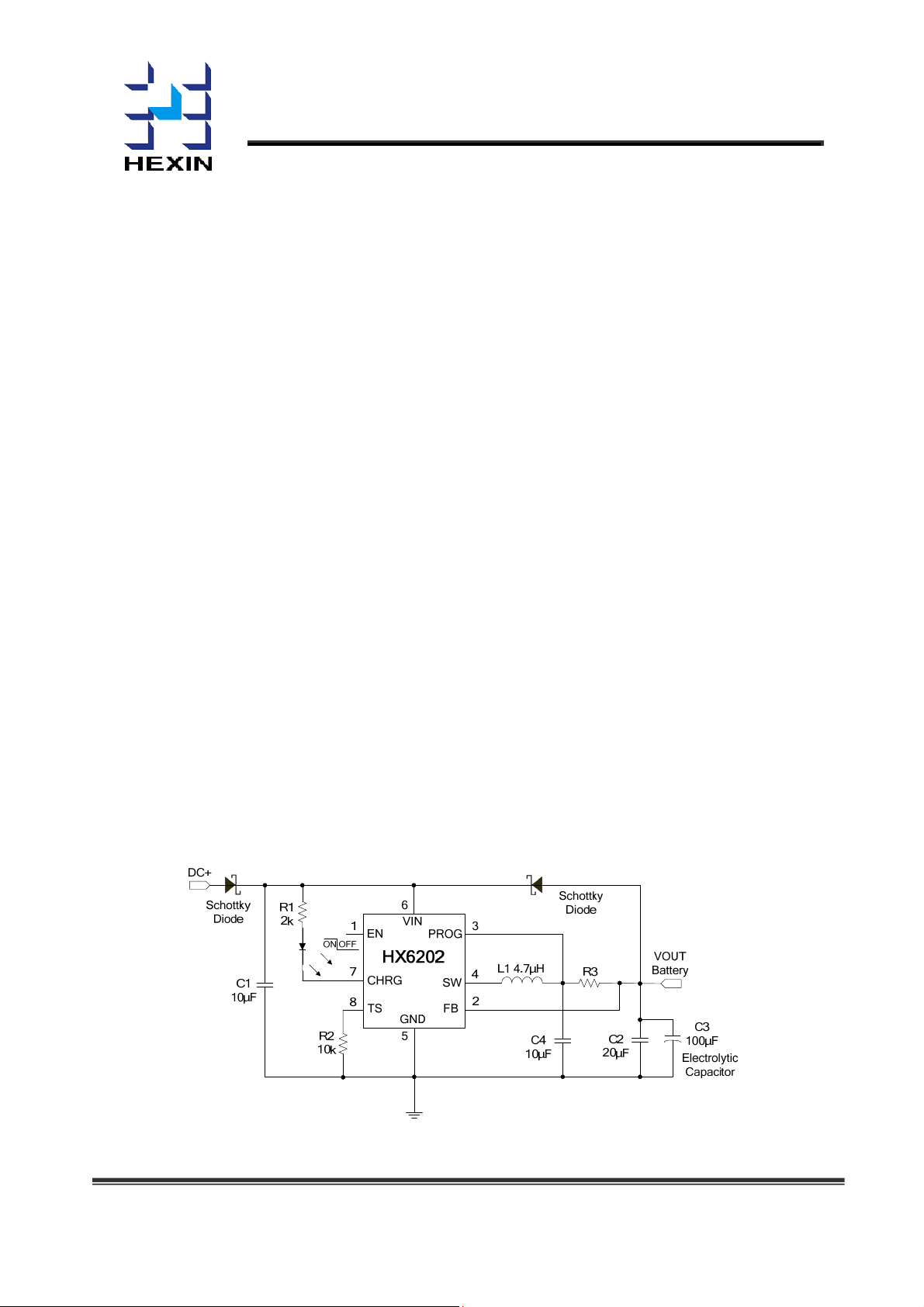
TTyyppiiccaall AApppplliiccaattiioonn CCiirrccuuiitt
*The charge current can be set by I
*This application circuit is for MID.
m
wwwwww..hhxxsseemmii..ccoom
= 0.17V/R3.
BAT
1

HHXX6622002
2
DC+
Schottky
Diode
C1
10uF
R1
2k
R2
10k
1
7
8
VIN
EN
CHRG
TS FB
GND
6
PROG
SW
5
3
4
2
Schottky
L1 4.7uH
*This application circuit is for backup source specially.
PPiinn AAssssiiggnnmmeenntt aanndd DDeessccrriippttiioonn
PIN NAME DESCRIPTION
1 EN
Diode
C4
10uF
Q1
R3
C2
20uF
R4
100k
R5
22k
Q2
C3
10uF
R6
10k
ON/OFF Control(High Enable)
VOUT
Battery
DC+
2 FB
Feedback
3 PROG Charge Current Program
4 SW
5 GND
6 VIN
7 CHRG Open-Drain Charge Status for Output
Switch Output
Ground
Input
8 TS Temperature Sense
s
AAbbssoolluuttee MMaaxxiimmuumm RRaattiinnggs
(Note 1)
VIN, CHRG, SW, PROG Voltage................................................................................. -0.3V ~ 6.5V
SW Pin Current ......................................................................................................................... 3.8A
Operating Temperature Range (Note 2)..................................................................... -40℃ ~ +85℃
Maximum Junction Temperature ........................................................................................... +150℃
Storage Temperature Range …………………………………………….....................-65℃ ~ +125℃
Lead Temperature (Soldering, 10 sec)....................................................................................+265℃
Note 1: Stresses listed as the above “Absolute Maximum Ratings” may cause permanent damage to the device.
Exposure to absolute maximum rating conditions for extended periods may remain possibility to affect device reliability.
Note 2: The HX6202 is guaranteed to meet performance specifications from 0C to 70C. Specifications over the –40C
to 85C operating temperature range are assured by design, characterization and correlation with statistical process
controls
wwwwww..hhxxsseemmii..ccoom
m
2
HHXX6622002
2
EElleeccttrriiccaall CChhaarraacctteerriissttiiccss
Operating Conditions: TA=25 , ℃ VIN=5V, unless otherwise specified.
SYMBOL PARAMETER CONDITIONS MIN TYP MAX UNITS
VIN Input Supply Voltage
4.7 5.0 6 V
Shutdown Mode 19 μA
IQ Input Supply Current
Sleep Mode 4 μA
V
ASD
f
OSC
DC Maximum Duty Cycle
Automatic Shutdown
Threshold Voltage
Switching Frequency I
VIN – V
BAT
150 mV
BAT
= 1A 1 MHz
100 %
Battery Voltage Regulation Constant-Current Charge
V
FLOAT
V
SNS(CHG)
Battery Regulated Float
Voltage
Constant Current Sense
Voltage
0 ≤TA≤85 , I℃℃
3V ≤ V
≤ 4V 170 mV
BAT
= 1.2A 4.17 4.22 4.26 V
OUT
Trickle Charge
Trickle Current Sense
V
SNS(TRIKL)
Voltage
Trickle Charge Threshold
V
TRIKL
Voltage
Battery Recharge Threshold
Recharge Battery
ΔV
RECHRG
Voltage Offset from Full
Charged Battery Voltage
TS Pin
TS Pin Threshold
V
V
TS- HOT
TS- COLD
Voltage (Hot)
TS Pin Threshold
Voltage (Cold)
ITS TS Pin Output Current V
V
= 0V 10 mV
BAT
V
Rising 2.9 V
BAT
V
BAT(FULLCHARGED)
V
Falling
BAT
Falling
V
TS
– V
Hysteresis
Rising
V
NTC
Hysteresis
= 0.85V 82 μA
TS
RECHRG
,
170 mV
0.54 V
2.36 V
wwwwww..hhxxsseemmii..ccoom
m
3
HHXX6622002
2
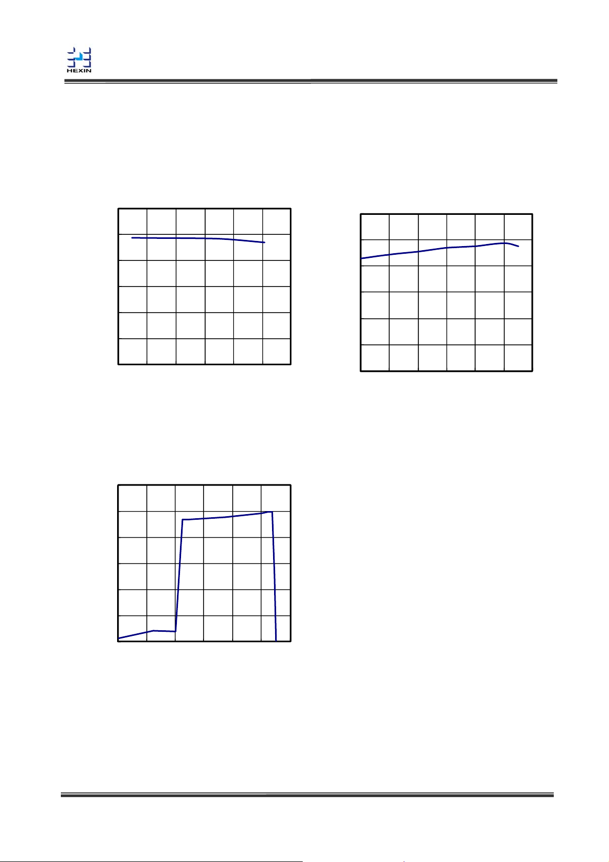
TTyyppiiccaall PPeerrffoorrmmaannccee CChhaarraacctteerriissttiiccss
Operating Conditions: TA = 25 ,℃ R3 = 0.33||0.33Ω, unless otherwise specified.
Efficiency vs Char ge Cur rent
=5V)
(V
IN
95%
90%
85%
80%
Eff iciency
75%
70%
65%
200 350 500 650 800 950 1100
I
(mA)
BAT
95%
90%
85%
80%
Eff iciency
75%
70%
65%
Efficiency vs Batter y Voltage
(V
3 3.2 3.4 3.6 3.8 4 4.2
V
IN
BAT
=5V)
(V)
Charge Cur r ent vs Battery Voltage
(V
=5V)
IN
1.2
1
0.8
(A)
0.6
BAT
I
0.4
0.2
0
2 2.4 2.8 3.2 3.6 4 4.4
V
(V)
BAT
wwwwww..hhxxsseemmii..ccoom
m
4
 Loading...