

Hexin HX3141 Schematics
DDCC//DDCC CCoonnvveerrtteerr
FFeeaattuurreess
AApppplliiccaattiioonnss
OOrrddeerriinngg IInnffoorrmmaattiioonn
TTiinnyy PPaacckkaaggee,, HHiigghh EEffffiicciieennccyy,, SStteepp--uupp
DDeessccrriippttiioonn
The HX3141 is a compact, high efficiency, and low
Output:1.8V-5.5V
Internal MOSFET with high switch current up to
3A
25µA Quiescent (Switch-off) Supply Current
Shutdown Mode Supply Current :<5uA
90% Efficiency
Up to 450KHz Switching Frequency
Using Internal Power Switches
SOT-23-6 Package
PDA
DSC
LCD Panel
RF-Tags
MP3
Portable Instrument
Wireless Equipment
voltage step-up DC/DC converter including an error
amplifier, ramp generator, comparator, switch pass
element and driver in which providing a stable and
high efficient operation over a wide range of load
currents. It operates in stable waveforms without
external compensation.
The low start-up input voltage below 1.1V. The high
switching rate minimized the size of external
components. Besides, the 25µA low quiescent
current together with high efficiency maintains long
battery lifetime.
The output voltage is set with two external resistors.
HX1001
HX3141
m
wwwwww..hhxxsseemmii..ccoom
1
HHXX3311441
1
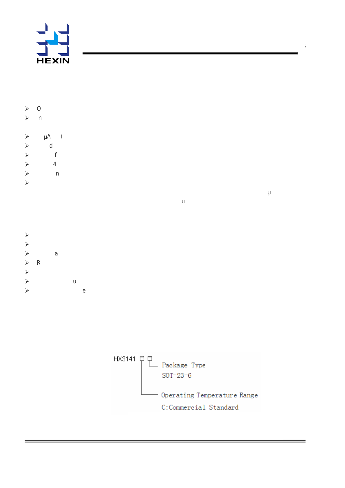
TTyyppiiccaall AApppplliiccaattiioonn
Figure.1 (1.1V Stat-up input Voltage
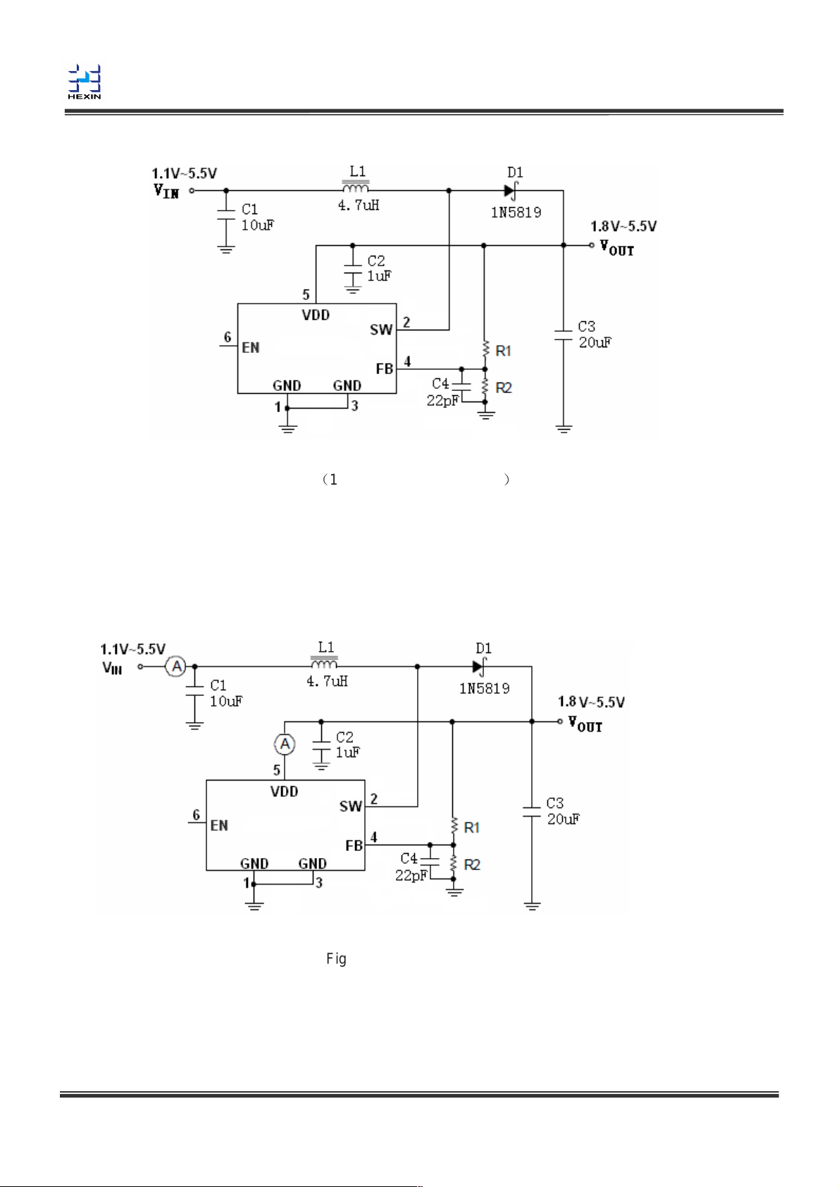
TTeesstt CCiirrccuuiitt
)
Figure. 2
wwwwww..hhxxsseemmii..ccoom
m
2
HHXX3311441
1
AAbbssoolluuttee MMaaxxiimmuumm RRaattiinnggss
Supply Voltage…………………………………………………………………….…−0.3V to 6V
SW Pin Switch Voltage……………………………………………………………………−0.3V to 6V
Other I/O Pin Voltages……………………………………………………………−0.3V to 6V
SW Pin Switch Current ……………………………………………………………...………………..3A
Operating Junction Temperature…………………………………………………….……………..125°C
Storage Temperature Range ……………………………………………….−65°C ~ +150°C
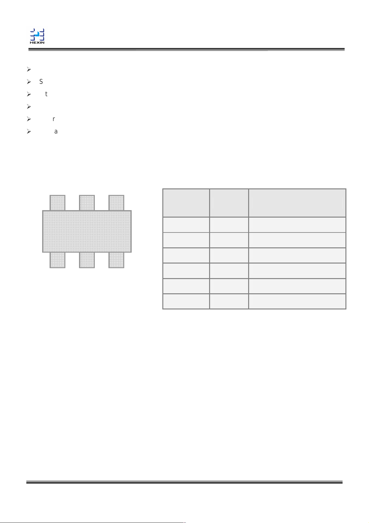
PPiinn AAssssiiggnnmmeenntt
6 5 4
PIN
NUMBER
DFN2*2-6
1 GND
PIN NAME
FUNCTION
Ground
2 SW
3 GND
1 2 3
4 FB
5 VDD
6 EN
ON/OFF Control(High Enable)
Switch Output
Ground
Feedback
Output
wwwwww..hhxxsseemmii..ccoom
m
3
 Loading...