

HEI HY628100AG-55, HY628100AG-70, HY628100AG-85, HY628100ALG-55, HY628100ALG-70 Datasheet
...
This document is a general product description and is subject to change without notice. Hyundai Electronics does not assume any
responsibility for use of circuits described. No patent licenses are implied.
Rev.05 /Feb.99 Hyundai Semiconductor
HY628100A Series
128Kx8bit CMOS SRAM
DESCRIPTION
The HY628100A is a high speed, low power and
1M bit CMOS Static Random Access Memory
organized as 131,072 words by 8bit. The
HY628100A uses high performance CMOS
process technology and designed for high speed
low power circuit technology. It is particulary well
suited for used in high density low power system
application. This device has a data retention
mode that guarantees data to remain valid at a
minimum power supply voltage of 2.0V.
FEATURES
• Fully static operation and Tri-state output
• TTL compatible inputs and outputs
• Battery backup(L/LL-part)
- 2.0V(min) data retention
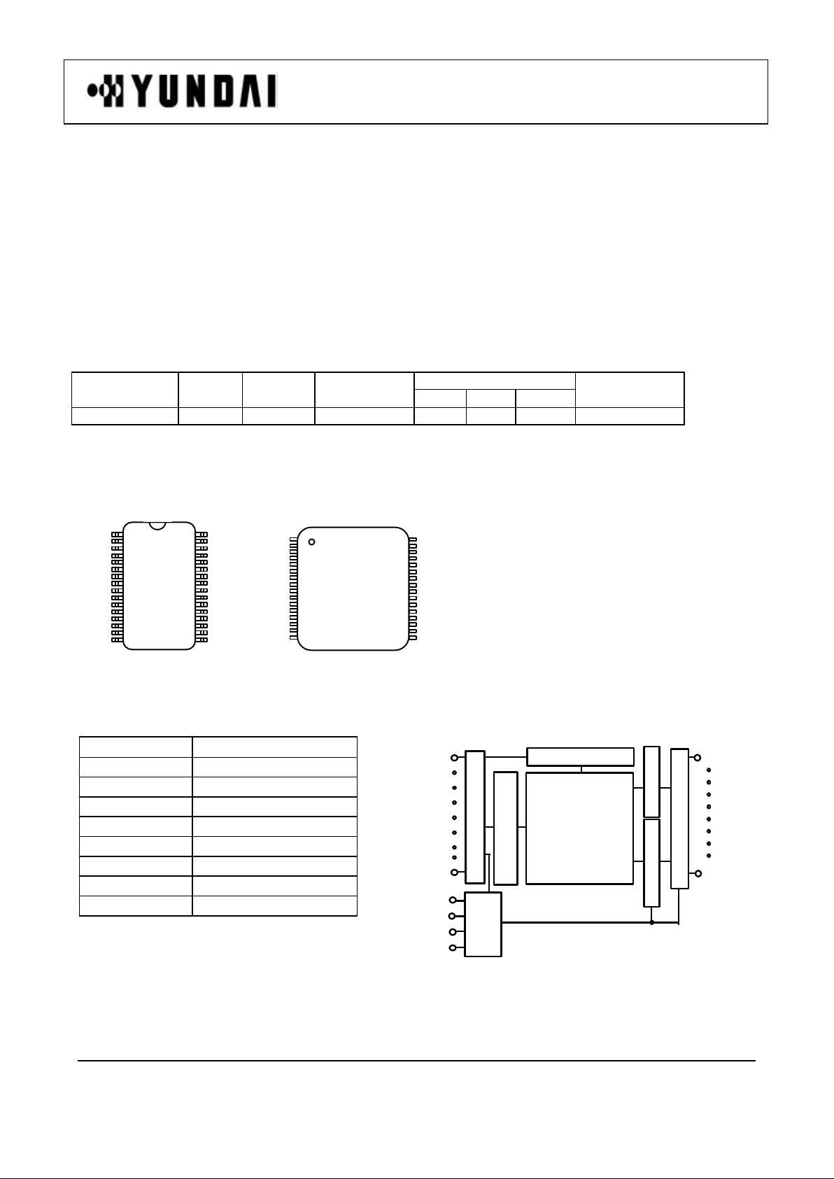
• Standard pin configuration
- 32pin 525mil SOP
- 32pin 8x20mm TSOP-I(Standard)
Product Voltage Speed Operation Standby Current(uA) Temperature
No (V) (ns) Current(mA) L LL
(°C)
HY628100A 5.0 55/70/85 10 1mA 100 20 0~70
Comment : 50ns is available with 30pF test load.
PIN CONNECTION
1
2
3
4
5
6
7
8
9
10
11
12
13
14
15
16
32
31
30
29
28
27
26
25
24
23
22
21
20
19
18
17
Vcc
A15
/WE
A13
A8
A9
A11
/OE
A10
/CS1
I/O8
I/O7
I/O6
I/O5
I/O4
NC
A16
A14
A12
A7
A6
A5
A4
A3
A2
A1
A0
I/O1
I/O2
I/O3
Vss
CS2
1
2
3
4
5
6
7
8
9
11
12
13
14
15
16
32
30
29
28
27
26
25
24
22
21
20
19
18
17
/OE
DQ8
DQ7
DQ6
DQ5
DQ4
Vss
DQ3
DQ1
A0
A1
A2
A3
A11
A9
A13
/WE
CS2
A15
Vcc
NC
A16
A12
A7
A6
A5
A4
/CS1
SOP TSOP-I(Standard)
PIN DESCRIPTION BLOCK DIAGRAM
Pin Name Pin Function
/CS1 Chip Select 1
CS2 Chip Select 2
/WE Write Enable
/OE Output Enable
A0 ~ A16 Address Input
I/O1 ~ I/O8 Data Input/Output
Vcc Power(5.0V)
Vss Ground
CS2
A16
COLUMN DECODER
A0
ROW DECODER
MEMORY ARRAY
1024x1024
SENSE AMP
OUTPUT BUFFER
I/O1
I/O8
ADD INPUT BUFFER
/CS1
/OE
/WE
WRITE DRIVER
CONTROL
LOGIC
HY628100A Series
Rev.05 /Feb.99
2
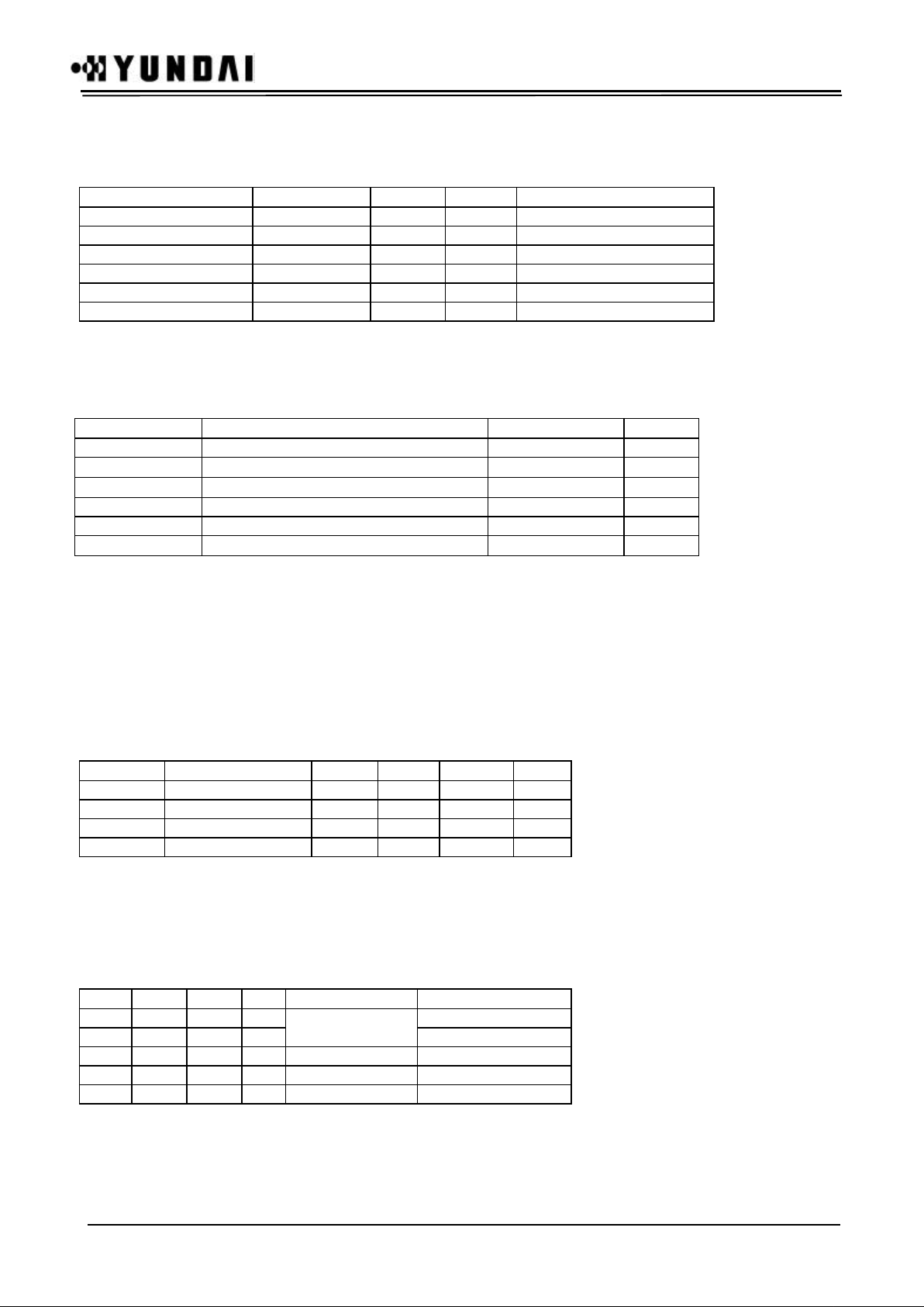
ORDERING INFORMATION
Part No. Speed Power Temp Package
HY628100AG 55/70/85 SOP
HY628100ALG 55/70/85 L-part SOP
HY628100ALLG 55/70/85 LL-part SOP
HY628100AT1 55/70/85 TSOP-I(Standard)
HY628100ALT1 55/70/85 L-part TSOP-I(Standard)
HY628100ALLT1 55/70/85 LL-part TSOP-I(Standard)
Comment : 50ns is available with 30pF test load.
ABSOLUTE MAXIMUM RATING (1)
Symbol Parameter Rating Unit
Vcc, VIN, VOUT Power Supply, Input/Output Voltage -0.5 to 7.0 V
TA Operating Temperature 0 to 70
°C
TSTG Storage Temperature -65 to 125
°C
PD Power Dissipation 1.0 W
IOUT Data Output Current 50 mA
TSOLDER Lead Soldering Temperature & Time
260 •10 °C•sec
Note
1. Stresses greater than those listed under ABSOLUTE MAXIMUM RATINGS may cause permanent
damage to the device. This is stress rating only and the functional operation of the device under these or
any other conditions above those indicated in the operation of this specification is not implied.
Exposure to the absolute maximum rating conditions for extended period may affect reliablity.
RECOMMENDED DC OPERATING CONDITION
TA=0°C to 700°C /-400°C to 85°C
Symbol Parameter Min. Typ. Max. Unit
Vcc Supply Voltage 4.5 5.0 5.5 V
Vss Ground 0 0 0 V
VIH Input High Voltage 2.2 - Vcc+0.5 V
VIL Input Low Voltage -0.5(1) - 0.8 V
Note :
1. VIL = -3.0V for pulse width less than 30ns
TRUTH TABLE
/CS1 CS2 /WE /OE MODE I/O OPERATION
H X X X Standby High-Z
X L X X High-Z
L H H H Output Disabled High-Z
L H H L Read Data Out
L H L X Write Data In
Note :
1. H=VIH, L=VIL, X=don't care
HY628100A Series
Rev.05 /Feb.99
3
DC ELECTRICAL CHARACTERISTICS
Vcc = 5.0V±10%, TA = 0°C to 70°C, unless otherwise specified
Symbol Parameter Test Condition Min. Typ. Max. Unit
ILI Input Leakage Current Vss < VIN < Vcc -1 - 1 uA
ILO Output Leakage Current Vss < VOUT < Vcc, /CS1 = VIH or
CS2 = VIL or /OE = VIH or /WE = VIL
-1 - 1 uA
Icc Operating Power Supply
Current
/CS1 = VIL, CS2 = VIH,
VIN = VIH or VIL, II/O = 0mA
- 5 10 mA
ICC1 Average Operating
Current
/CS1 = VIL CS2 = VIH,
Min Duty Cycle = 100%, II/O = 0mA
- 30 50 mA
ISB TTL Standby Current
(TTL Input)
/CS1 = VIH or CS2 = VIL - 1 2 mA
ISB1 Standby Current /CS1 > Vcc - 0.2V - - 1 mA
(CMOS Input) CS2 > 0.2V or L - 2 100 uA
CS2 > Vcc - 0.2V LL - 1 20 uA
VOL Output Low Voltage IOL = 2.1Ma - - 0.4 V
VOH Output High Voltage IOH = -1mA 2.4 - - V
Note : Typical values are at Vcc = 5.0V, TA = 25°C
AC CHARACTERISTICS
Vcc = 5.0V±10%, TA = 0°C to 70°C (Normal), unless otherwise specified
-55 -70 -85
Min. Max. Min. Max. Min Max.
1 TRC Read Cycle Time 55 - 70 - 85 - ns
2 tAA* Address Access Time - 55 - 70 - 85 ns
3 tACS* Chip Select Access Time - 55 - 70 - 85 ns
4 TOE Output Enable to Output Valid - 25 - 35 - 45 ns
5 TCLZ Chip Select to Output in Low Z 10 - 10 - 10 - ns
6 TOLZ Output Enable to Output in Low Z 5 - 5 - 5 - ns
7 tCHZ Chip Deselection to Output in High Z 0 20 0 25 0 30 ns
8 tOHZ Out Disable to Output in High Z 0 20 0 25 0 30 ns
9 tOH Output Hold from Address Change 10 - 10 - 10 - ns
10 tWC Write Cycle Time 55 - 70 - 85 - ns
11 tCW Chip Selection to End of Write 45 - 60 - 70 - ns
12 tAW Address Valid to End of Write 45 - 60 - 70 - ns
13 tAS Address Set-up Time 0 - 0 - 0 - ns
14 tWP Write Pulse Width 40 - 50 - 55 - ns
15 tWR Write Recovery Time 0 - 0 - 0 - ns
16 tWHZ Write to Output in High Z 0 20 0 25 0 30 ns
17 tDW Data to Write Time Overlap 25 - 30 - 35 - ns
18 tDH Data Hold from Write Time 0 - 0 - 0 - ns
19 tOW Output Active from End of Write 5 - 5 - 5 - ns
Comment : tAA* and tACS* can meet 50ns with 30pF test load.
READ CYCLE
WRITE CYCLE
Symbol
Parameter
#
Unit
 Loading...