

HEI HM17CM256 Datasheet
- 1 -
HM17CM256
128XRGBX82 OUTPUT LCD DRIVER IC
with built-in RAM
■
INSTRUCTION
HM17CM256 is a dot-Matrix LCD drive IC with 82
commons (80 + 2 icons) and 384 segments (128 X
RGB) drive ports for 256 colors driving.
This IC stores the serial or parallel BIT data
transferred by the microcomputer on the built-in
RAM (81,920 bits for graphic + 2048 bits for icons)
and generates the signals to drive LCD panel.
Color graphic display is achieved by selecting 8
gray (256 color) levels out of 32 gray palettes
independently.
This IC is suitable for battery-operated system,
hand-carrying information equipment by ensuring
low power consumption, low power supply (1.7V ~ )
and a wide range of operating voltage.
And 164 x 128 display (maximum) is possible with
master and slave application.
■
FEATURES
256 color bitmap LCD driver
LCD drive outputs 128×RGB segments, 80 commons for graphic and 2 commons for icons
Display RAM capacity 81,920bits (for graphic usage)
2,048bits (for icon usage)
Gradation display 8 gradations can be selected from 32 gradations by PWM control
Black/White display 82 × (128 × 3) bits display is possible
8 bit BUS interface directly connectable with 68 / 80 series CPU
RAM data length 8 BIT / 16 BIT selectable
Serial interface available
Programmable duty / bias ratio with command
Various instruction set
display data read/write, display ON/OFF, positive/negative display, page address set
display start line address set, partial display, bias select,
column address set, all display ON/OFF, boosting selection, n line inversion mode
read modified write, power save …
Built-in voltage booster (programmable) : 7 × boosting
Built-in voltage regulator
Controllable contrast with built-in electric volume (128 steps)
Low current consumption
Logic supply 1.7V ~ 3.3V
LCD drive supply 5.0V ~ 18.0V
C-MOS silicon process
Package bumped chip / bare chip
Preliminary Specification(0.3)
HM17CM256
EXTERNAL SHAPE
01/02/09
HM17CM256
- 2 -
PAD LAYOUT
note 1) The (L) (R) (C) mark after port name is internally shorted.
note 2) DMYport is opened electrically.
chip center : X= 0
µµ
m, Y= 0µµm
chip size : with scribe lane : 19.84mm x 2.48mm ,
main chip : 19.74mm x 2.38mm
chip thickness : 625µµm ±± 25µµm
bump size : 100µµm x 32µµm, 100µµm x 80µµm
bump pitch : 50µµm(Min)
bump height : 18 ±± 3µµm
bump material : Au
align mark appearance and size
a : 30µµm
b : 6µµm
c : 120µµm
d : 27µµm
coordinates of align marks
(X= - 9732µµm, Y= -1052µµm)
(X= 9732µµm, Y= -1052µµm)
1
DMY
5
(R)
SEGA
125
DMY
5
(L)
SEGB
125
SEGC
125
SEGA
126
SEGB
126
SEGC
126
SEGA
127
SEGB
127
SEGC
127
COM40
SEGSC3
SEGSA2
DMY6(R)
DMY6(L)
DMY7(R)
DMY7(L)
COM66
DMY
0
(R)
DMY
0
(L)
COM
67
RES
COM
79
CLK
FR
FLM
CL
V
SS
(R)
V
SS
(C)
V
SS
(L)
D
15
D
13
D
12
D
14
D
11
D
10
D
9
D
8
D
7
D
6
D
5
D
4
/SPOL
D
3
/SMODE
D
2
/EXCS
D
1
/SDA
D
0
/SCL
V
DD
(R)
V
DD
(C)
V
DD
(L)
RD
WR
V
SSA
(R)
V
SSA
(C)
SEL68
V
SSA
(L)
P/S
V
DDA
M/S
V
SS
(R)
V
SS
(C)
RS
V
SS
(L)
CSB
V
DD
(R)
V
DD
(C)
V
DD
(L)
TEST
V
SSA
(R)
V
SSA
(C)
COMI
1
V
SSA
(L)
HM17CM256
- 3 -
All sorts of PAD open
1. open size (e, f)=(66, 86)
17~118
2. open size (e, f)=(18, 86)
1~16, 119~596
Original point mark of left picture is presented
at the table of pad coordinates.
unit
µµ
m
DMY2(L)
DMY2(R)
COM25
COM0
COMI0
SEGSA0
SEGSC1
DMY3(L)
DMY3(R)
DMY
4
(R)
SEGA
0
DMY
4
(L)
SEGB
0
SEGC
0
SEGA
1
SEGB
1
SEGC
1
SEGA
2
SEGB
2
SEGC
2
X
Y
COM
39
V
EE
(R)
V
EE
(C)
V
EE
(L)
V
REF
V
BA
(R)
V
BA
(L)
V
REG
(R)
V
REG
(L)
C
1
+(R)
C
1
+(L)
V
SSH
(R)
V
SSH
(C)
OSC
2
V
SSH
(L)
OSC
1
V
LCD
(L)
V
LCD
(R)
V
1
(L)
V
1
(R)
V
2
(L)
V
2
(R)
V
3
(L)
V
3
(R)
V
4
(L)
V
4
(R)
V
SSH
(R)
V
SSH
(C)
V
SSH
(L)
C
1
-(R)
C
1
-(L)
C
2
+(R)
C
2
+(L)
C
2
-(R)
C
2
-(L)
C
3
+(R)
C
3
+(L)
C
3
-(R)
C
3
-(L)
C
4
+(R)
C
4
+(L)
C
4
-(R)
C
4
-(L)
C
5
+(R)
C
5
+(L)
C
5
-(R)
C
5
-(L)
C
6
+(R)
C
6
+(L)
C
6
-(R)
C
6
-(L)
V
OUT
(R)
V
OUT
(L)
V
LCD
(L)
V
LCD
(R)
DMY
1
(L)
COM
26
DMY
1
(R)
HM17CM256
- 4 -
■
PAD coordinates 1
chip size 19840µm x 2480µm ( chip center : 0µm x 0µm )
PAD
No.
Pin name
X(µm)
Y(µm)
PAD
No.
Pin name
X (µm)
Y (µm)
PAD
No.
Pin name
X (µm)
Y (µm)
1
DMY0(L)
-9625
-1068
52
D10
-2550
-1068
103
C4+(L)
6120
-1068
2
DMY0(R)
-9575
-1068
53
D11
-2380
-1068
104
C4+(R)
6290
-1068
3
COM67
-9525
-1068
54
D12
-2210
-1068
105
C4-(L)
6460
-1068
4
COM68
-9475
-1068
55
D13
-2040
-1068
106
C4-(R)
6630
-1068
5
COM69
-9425
-1068
56
D14
-1870
-1068
107
C5+(L)
6800
-1068
6
COM70
-9375
-1068
57
D15
-1700
-1068
108
C5+(R)
6970
-1068
7
COM71
-9325
-1068
58
VSS(L)
-1472
-1068
109
C5-(L)
7140
-1068
8
COM72
-9275
-1068
59
VSS(C)
-1340
-1068
110
C5-(R)
7310
-1068
9
COM73
-9225
-1068
60
VSS(R)
-1190
-1068
111
C6+(L)
7480
-1068
10
COM74
-9175
-1068
61
CL
-1020
-1068
112
C6+(R)
7650
-1068
11
COM75
-9125
-1068
62
FLM
-850
-1068
113
C6-(L)
7820
-1068
12
COM76
-9075
-1068
63
FR
-680
-1068
114
C6-(R)
7990
-1068
13
COM77
-9025
-1068
64
CLK
-510
-1068
115
V
LCD
(L)
8160
-1068
14
COM78
-8975
-1068
65
OSC1
-340
-1068
116
V
LCD
(R)
8330
-1068
15
COM79
-8925
-1068
66
OSC2
-107
-1068
117
V
OUT
(L)
8500
-1068
16
COMI1
-8875
-1068
67
V
SSH
(L)
74
-1068
118
V
OUT
(R)
8670
-1068
17
V
SSA
(L)
-8670
-1068
68
V
SSH
(C)
196
-1068
119
COM39
8875
-1068
18
V
SSA
(C)
-8500
-1068
69
V
SSH
(R)
318
-1068
120
COM38
8925
-1068
19
V
SSA
(R)
-8330
-1068
70
V
LCD
(L)
510
-1068
121
COM37
8975
-1068
20
TEST
-8171
-1068
71
V
LCD
(R)
680
-1068
122
COM36
9025
-1068
21
VDD(L)
-7990
-1068
72
V1(L)
850
-1068
123
COM35
9075
-1068
22
VDD(C)
-7820
-1068
73
V1(R)
1020
-1068
124
COM34
9125
-1068
23
VDD(R)
-7650
-1068
74
V2(L)
1190
-1068
125
COM33
9175
-1068
24
RES
-7480
-1068
75
V2(R)
1360
-1068
126
COM32
9225
-1068
25
CS
-7310
-1068
76
V3(L)
1530
-1068
127
COM31
9275
-1068
26
RS
-7140
-1068
77
V3(R)
1700
-1068
128
COM30
9325
-1068
27
VSS(L)
-6970
-1068
78
V4(L)
1870
-1068
129
COM29
9375
-1068
28
VSS(C)
-6800
-1068
79
V4(R)
2040
-1068
130
COM28
9425
-1068
29
VSS(R)
-6630
-1068
80
V
REG
(L)
2210
-1068
131
COM27
9475
-1068
30
M/S
-6448
-1068
81
V
REG
(R)
2380
-1068
132
COM26
9525
-1068
31
V
DDA
-6290
-1068
82
VBA(L)
2550
-1068
133
DMY1(L)
9575
-1068
32
P/S
-6120
-1068
83
VBA(R)
2693
-1068
134
DMY1(R)
9625
-1068
33
SEL68
-5950
-1068
84
V
REF
2879
-1068
135
DMY2(L)
9726
-900
34
V
SSA
(L)
-5780
-1068
85
VEE(L)
3060
-1068
136
DMY2(R)
9726
-850
35
V
SSA
(C)
-5610
-1068
86
VEE(C)
3230
-1068
137
COM25
9726
-800
36
V
SSA
(R)
-5440
-1068
87
VEE(R)
3400
-1068
138
COM24
9726
-750
37
WR
-5270
-1068
88
V
SSH
(L)
3570
-1068
139
COM23
9726
-700
38
RD
-5111
-1068
89
V
SSH
(C)
3740
-1068
140
COM22
9726
-650
39
VDD(L)
-4930
-1068
90
V
SSH
(R)
3910
-1068
141
COM21
9726
-600
40
VDD(C)
-4760
-1068
91
C1+(L)
4102
-1068
142
COM20
9726
-550
41
VDD(R)
-4590
-1068
92
C1+(R)
4250
-1068
143
COM19
9726
-500
42
D0/SCL
-4420
-1068
93
C1-(L)
4420
-1068
144
COM18
9726
-450
43
D1/SDA
-4250
-1068
94
C1-(R)
4590
-1068
145
COM17
9726
-400
44
D2/EXCS
-3995
-1068
95
C2+(L)
4760
-1068
146
COM16
9726
-350
45
D3/SMODE
-3740
-1068
96
C2+(R)
4930
-1068
147
COM15
9726
-300
46
D4/SPOL
-3570
-1068
97
C2-(L)
5100
-1068
148
COM14
9726
-250
47
D5
-3400
-1068
98
C2-(R)
5270
-1068
149
COM13
9726
-200
48
D6
-3230
-1068
99
C3+(L)
5440
-1068
150
COM12
9726
-150
49
D7
-3060
-1068
100
C3+(R)
5610
-1068
151
COM11
9726
-100
50
D8
-2890
-1068
101
C3-(L)
5780
-1068
152
COM10
9726
-50
51
D9
-2720
-1068
102
C3-(R)
5950
-1068
153
COM9
9726
0
HM17CM256
- 5 -
■
PAD coordiantes 2
chip size 19840µm x 2480µm ( chip center : 0µm x 0µm )
PAD
No.
Pin name
X(µm)
Y(µm)
PAD
No.
Pin name
X (µm)
Y (µm)
PAD
No.
Pin name
X (µm)
Y (µm)
154
COM8
9726
50
205
SEGB10
8025
1068
256
SEGB27
5475
1068
155
COM7
9726
100
206
SEGC10
7975
1068
257
SEGC27
5425
1068
156
COM6
9726
150
207
SEGA11
7925
1068
258
SEGA28
5375
1068
157
COM5
9726
200
208
SEGB11
7875
1068
259
SEGB28
5325
1068
158
COM4
9726
250
209
SEGC11
7825
1068
260
SEGC28
5275
1068
159
COM3
9726
300
210
SEGA12
7775
1068
261
SEGA29
5225
1068
160
COM2
9726
350
211
SEGB12
7725
1068
262
SEGB29
5175
1068
161
COM1
9726
400
212
SEGC12
7675
1068
263
SEGC29
5125
1068
162
COM0
9726
450
213
SEGA13
7625
1068
264
SEGA30
5075
1068
163
COMI0
9726
500
214
SEGB13
7575
1068
265
SEGB30
5025
1068
164
SEGSA0
9726
550
215
SEGC13
7525
1068
266
SEGC30
4975
1068
165
SEGSB0
9726
600
216
SEGA14
7475
1068
267
SEGA31
4925
1068
166
SEGSC0
9726
650
217
SEGB14
7425
1068
268
SEGB31
4875
1068
167
SEGSA1
9726
700
218
SEGC14
7375
1068
269
SEGC31
4825
1068
168
SEGSB1
9726
750
219
SEGA15
7325
1068
270
SEGA32
4775
1068
169
SEGSC1
9726
800
220
SEGB15
7275
1068
271
SEGB32
4725
1068
170
DMY3(L)
9726
850
221
SEGC15
7225
1068
272
SEGC32
4675
1068
171
DMY3(R)
9726
900
222
SEGA16
7175
1068
273
SEGA33
4625
1068
172
DMY4(L)
9675
1068
223
SEGB16
7125
1068
274
SEGB33
4575
1068
173
DMY4(R)
9625
1068
224
SEGC16
7075
1068
275
SEGC33
4525
1068
174
SEGA0
9575
1068
225
SEGA17
7025
1068
276
SEGA34
4475
1068
175
SEGB0
9525
1068
226
SEGB17
6975
1068
277
SEGB34
4425
1068
176
SEGC0
9475
1068
227
SEGC17
6925
1068
278
SEGC34
4375
1068
177
SEGA1
9425
1068
228
SEGA18
6875
1068
279
SEGA35
4325
1068
178
SEGB1
9375
1068
229
SEGB18
6825
1068
280
SEGB35
4275
1068
179
SEGC1
9325
1068
230
SEGC18
6775
1068
281
SEGC35
4225
1068
180
SEGA2
9275
1068
231
SEGA19
6725
1068
282
SEGA36
4175
1068
181
SEGB2
9225
1068
232
SEGB19
6675
1068
283
SEGB36
4125
1068
182
SEGC2
9175
1068
233
SEGC19
6625
1068
284
SEGC36
4075
1068
183
SEGA3
9125
1068
234
SEGA20
6575
1068
285
SEGA37
4025
1068
184
SEGB3
9075
1068
235
SEGB20
6525
1068
286
SEGB37
3975
1068
185
SEGC3
9025
1068
236
SEGC20
6475
1068
287
SEGC37
3925
1068
186
SEGA4
8975
1068
237
SEGA21
6425
1068
288
SEGA38
3875
1068
187
SEGB4
8925
1068
238
SEGB21
6375
1068
289
SEGB38
3825
1068
188
SEGC4
8875
1068
239
SEGC21
6325
1068
290
SEGC38
3775
1068
189
SEGA5
8825
1068
240
SEGA22
6275
1068
291
SEGA39
3725
1068
190
SEGB5
8775
1068
241
SEGB22
6225
1068
292
SEGB39
3675
1068
191
SEGC5
8725
1068
242
SEGC22
6175
1068
293
SEGC39
3625
1068
192
SEGA6
8675
1068
243
SEGA23
6125
1068
294
SEGA40
3575
1068
193
SEGB6
8625
1068
244
SEGB23
6075
1068
295
SEGB40
3525
1068
194
SEGC6
8575
1068
245
SEGC23
6025
1068
296
SEGC40
3475
1068
195
SEGA7
8525
1068
246
SEGA24
5975
1068
297
SEGA41
3425
1068
196
SEGB7
8475
1068
247
SEGB24
5925
1068
298
SEGB41
3375
1068
197
SEGC7
8425
1068
248
SEGC24
5875
1068
299
SEGC41
3325
1068
198
SEGA8
8375
1068
249
SEGA25
5825
1068
300
SEGA42
3275
1068
199
SEGB8
8325
1068
250
SEGB25
5775
1068
301
SEGB42
3225
1068
200
SEGC8
8275
1068
251
SEGC25
5725
1068
302
SEGC42
3175
1068
201
SEGA9
8225
1068
252
SEGA26
5675
1068
303
SEGA43
3125
1068
202
SEGB9
8175
1068
253
SEGB26
5625
1068
304
SEGB43
3075
1068
203
SEGC9
8125
1068
254
SEGC26
5575
1068
305
SEGC43
3025
1068
204
SEGA10
8075
1068
255
SEGA27
5525
1068
306
SEGA44
2975
1068
HM17CM256
- 6 -
PAD coordinates 3
chip size 19840µm x 2480µm (chip center : 0µm x 0µm )
PAD
No.
Pin name
X(µm)
Y(µm)
PAD
No.
Pin name
X (µm)
Y (µm)
PAD
No.
Pin name
X (µm)
Y (µm)
307
SEGB44
2925
1068
358
SEGB61
375
1068
409
SEGB78
-2175
1068
308
SEGC44
2875
1068
359
SEGC61
325
1068
410
SEGC78
-2225
1068
309
SEGA45
2825
1068
360
SEGA62
275
1068
411
SEGA79
-2275
1068
310
SEGB45
2775
1068
361
SEGB62
225
1068
412
SEGB79
-2325
1068
311
SEGC45
2725
1068
362
SEGC62
175
1068
413
SEGC79
-2375
1068
312
SEGA46
2675
1068
363
SEGA63
125
1068
414
SEGA80
-2425
1068
313
SEGB46
2625
1068
364
SEGB63
75
1068
415
SEGB80
-2475
1068
314
SEGC46
2575
1068
365
SEGC63
25
1068
416
SEGC80
-2525
1068
315
SEGA47
2525
1068
366
SEGA64
-25
1068
417
SEGA81
-2575
1068
316
SEGB47
2475
1068
367
SEGB64
-75
1068
418
SEGB81
-2625
1068
317
SEGC47
2425
1068
368
SEGC64
-125
1068
419
SEGC81
-2675
1068
318
SEGA48
2375
1068
369
SEGA65
-175
1068
420
SEGA82
-2725
1068
319
SEGB48
2325
1068
370
SEGB65
-225
1068
421
SEGB82
-2775
1068
320
SEGC 48
2275
1068
371
SEGC65
-275
1068
422
SEGC82
-2825
1068
321
SEGA49
2225
1068
372
SEGA66
-325
1068
423
SEGA83
-2875
1068
322
SEGB49
2175
1068
373
SEGB66
-375
1068
424
SEGB83
-2925
1068
323
SEGC49
2125
1068
374
SEGC66
-425
1068
425
SEGC83
-2975
1068
324
SEGA50
2075
1068
375
SEGA67
-475
1068
426
SEGA84
-3025
1068
325
SEGB50
2025
1068
376
SEGB67
-525
1068
427
SEGB84
-3075
1068
326
SEGC50
1975
1068
377
SEGC67
-575
1068
428
SEGC84
-3125
1068
327
SEGA51
1925
1068
378
SEGA68
-625
1068
429
SEGA85
-3175
1068
328
SEGB51
1875
1068
379
SEGB68
-675
1068
430
SEGB85
-3225
1068
329
SEGC51
1825
1068
380
SEGC68
-725
1068
431
SEGC85
-3275
1068
330
SEGA52
1775
1068
381
SEGA69
-775
1068
432
SEGA86
-3325
1068
331
SEGB52
1725
1068
382
SEGB69
-825
1068
433
SEGB86
-3375
1068
332
SEGC52
1675
1068
383
SEGC69
-875
1068
434
SEGC86
-3425
1068
333
SEGA53
1625
1068
384
SEGA70
-925
1068
435
SEGA87
-3475
1068
334
SEGB53
1575
1068
385
SEGB70
-975
1068
436
SEGB87
-3525
1068
335
SEGC53
1525
1068
386
SEGC70
-1025
1068
437
SEGC87
-3575
1068
336
SEGA54
1475
1068
387
SEGA71
-1075
1068
438
SEGA88
-3625
1068
337
SEGB54
1425
1068
388
SEGB71
-1125
1068
439
SEGB88
-3675
1068
338
SEGC54
1375
1068
389
SEGC71
-1175
1068
440
SEGC88
-3725
1068
339
SEGA55
1325
1068
390
SEGA72
-1225
1068
441
SEGA89
-3775
1068
340
SEGB55
1275
1068
391
SEGB72
-1275
1068
442
SEGB89
-3825
1068
341
SEGC55
1225
1068
392
SEGC72
-1325
1068
443
SEGC89
-3875
1068
342
SEGA56
1175
1068
393
SEGA73
-1375
1068
444
SEGA90
-3925
1068
343
SEGB56
1125
1068
394
SEGB73
-1425
1068
445
SEGB90
-3975
1068
344
SEGC56
1075
1068
395
SEGC73
-1475
1068
446
SEGC90
-4025
1068
345
SEGA57
1025
1068
396
SEGA74
-1525
1068
447
SEGA91
-4075
1068
346
SEGB57
975
1068
397
SEGB74
-1575
1068
448
SEGB91
-4125
1068
347
SEGC57
925
1068
398
SEGC74
-1625
1068
449
SEGC91
-4175
1068
348
SEGA58
875
1068
399
SEGA75
-1675
1068
450
SEGA92
-4225
1068
349
SEGB58
825
1068
400
SEGB75
-1725
1068
451
SEGB92
-4275
1068
350
SEGC58
775
1068
401
SEGC75
-1775
1068
452
SEGC92
-4325
1068
351
SEGA59
725
1068
402
SEGA76
-1825
1068
453
SEGA93
-4375
1068
352
SEGB59
675
1068
403
SEGB76
-1875
1068
454
SEGB93
-4425
1068
353
SEGC59
625
1068
404
SEGC76
-1925
1068
455
SEGC93
-4475
1068
354
SEGA60
575
1068
405
SEGA77
-1975
1068
456
SEGA94
-4525
1068
355
SEGB60
525
1068
406
SEGB77
-2025
1068
457
SEGB94
-4575
1068
356
SEGC60
475
1068
407
SEGC77
-2075
1068
458
SEGC94
-4625
1068
357
SEGA61
425
1068
408
SEGA78
-2125
1068
459
SEGA95
-4675
1068

HM17CM256
- 7 -
■
PAD coordinates 4
chip size 19840µm x 2480µm (chip center : 0µm x 0µm )
PAD
No.
Pin name
X(µm)
Y(µm)
PAD
No.
Pin name
X (µm)
Y (µm)
PAD
No.
Pin name
X (µm)
Y (µm)
460
SEGB95
-4725
1068
511
SEGB
112
-7275
1068
562
SEGSA2
-9726
800
461
SEGC95
-4775
1068
512
SEGC
112
-7325
1068
563
SEGSB2
-9726
750
462
SEGA96
-4825
1068
513
SEGA
113
-7375
1068
564
SEGSC2
-9726
700
463
SEGB96
-4875
1068
514
SEGB
113
-7425
1068
565
SEGSA3
-9726
650
464
SEGC96
-4925
1068
515
SEGC
113
-7475
1068
566
SEGSB3
-9726
600
465
SEGA97
-4975
1068
516
SEGA
114
-7525
1068
567
SEGSC3
-9726
550
466
SEGB97
-5025
1068
517
SEGB
114
-7575
1068
568
COM40
-9726
500
467
SEGC97
-5075
1068
518
SEGC
114
-7625
1068
569
COM41
-9726
450
468
SEGA98
-5125
1068
519
SEGA
115
-7675
1068
570
COM42
-9726
400
469
SEGB98
-5175
1068
520
SEGB
115
-7725
1068
571
COM43
-9726
350
470
SEGC98
-5225
1068
521
SEGC
115
-7775
1068
572
COM44
-9726
300
471
SEGA99
-5275
1068
522
SEGA
116
-7825
1068
573
COM45
-9726
250
472
SEGB99
-5325
1068
523
SEGB
116
-7875
1068
574
COM46
-9726
200
473
SEGC99
-5375
1068
524
SEGC
116
-7925
1068
575
COM47
-9726
150
474
SEGA
100
-5425
1068
525
SEGA
117
-7975
1068
576
COM48
-9726
100
475
SEGB
100
-5475
1068
526
SEGB
117
-8025
1068
577
COM49
-9726
50
476
SEGC
100
-5525
1068
527
SEGC
117
-8075
1068
578
COM50
-9726
0
477
SEGA
101
-5575
1068
528
SEGA
118
-8125
1068
579
COM51
-9726
-50
478
SEGB
101
-5625
1068
529
SEGB
118
-8175
1068
580
COM52
-9726
-100
479
SEGC
101
-5675
1068
530
SEGC
118
-8225
1068
581
COM53
-9726
-150
480
SEGA
102
-5725
1068
531
SEGA
119
-8275
1068
582
COM54
-9726
-200
481
SEGB
102
-5775
1068
532
SEGB
119
-8325
1068
583
COM55
-9726
-250
482
SEGC
102
-5825
1068
533
SEGC
119
-8375
1068
584
COM56
-9726
-300
483
SEGA
103
-5875
1068
534
SEGA
120
-8425
1068
585
COM57
-9726
-350
484
SEGB
103
-5925
1068
535
SEGB
120
-8475
1068
586
COM58
-9726
-400
485
SEGC
103
-5975
1068
536
SEGC
120
-8525
1068
587
COM59
-9726
-450
486
SEGA
104
-6025
1068
537
SEGA
121
-8575
1068
588
COM60
-9726
-500
487
SEGB
104
-6075
1068
538
SEGB
121
-8625
1068
589
COM61
-9726
-550
488
SEGC
104
-6125
1068
539
SEGC
121
-8675
1068
590
COM62
-9726
-600
489
SEGA
105
-6175
1068
540
SEGA
122
-8725
1068
591
COM63
-9726
-650
490
SEGB
105
-6225
1068
541
SEGB
122
-8775
1068
592
COM64
-9726
-700
491
SEGC
105
-6275
1068
542
SEGC
122
-8825
1068
593
COM65
-9726
-750
492
SEGA
106
-6325
1068
543
SEGA
123
-8875
1068
594
COM66
-9726
-800
493
SEGB
106
-6375
1068
544
SEGB
123
-8925
1068
595
DMY7(L)
-9726
-850
494
SEGC
106
-6425
1068
545
SEGC
123
-8975
1068
596
DMY7(R)
-9726
-900
495
SEGA
107
-6475
1068
546
SEGA
124
-9025
1068
496
SEGB
107
-6525
1068
547
SEGB
124
-9075
1068
497
SEGC
107
-6575
1068
548
SEGC
124
-9125
1068
498
SEGA
108
-6625
1068
549
SEGA
125
-9175
1068
499
SEGB
108
-6675
1068
550
SEGB
125
-9225
1068
500
SEGC
108
-6725
1068
551
SEGC
125
-9275
1068
501
SEGA
109
-6775
1068
552
SEGA
126
-9325
1068
502
SEGB
109
-6825
1068
553
SEGB
126
-9375
1068
503
SEGC
109
-6875
1068
554
SEGC
126
-9425
1068
504
SEGA
110
-6925
1068
555
SEGA
127
-9475
1068
505
SEGB
110
-6975
1068
556
SEGB
127
-9525
1068
506
SEGC
110
-7025
1068
557
SEGC
127
-9575
1068
507
SEGA
111
-7075
1068
558
DMY5(L)
-9625
1068
508
SEGB
111
-7125
1068
559
DMY5(R)
-9675
1068
509
SEGC
111
-7175
1068
560
DMY6(L)
-9726
900
510
SEGA
112
-7225
1068
561
DMY6(R)
-9726
850
HM17CM256
- 8 -
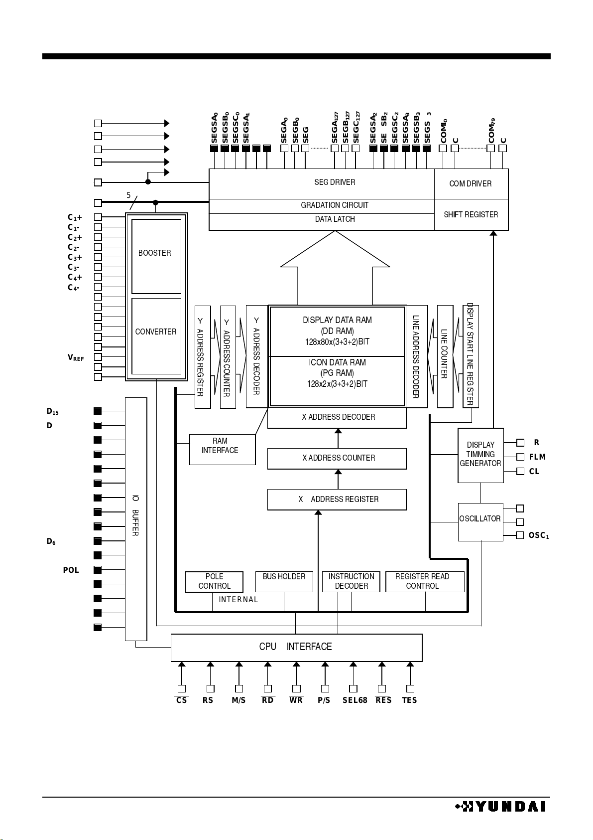
BLOCK DIAGRAM
VSS
VDD
V
LCD
, V1 ~V4
V
OUT
VBA
VEE
INTERNAL BUS
CLK
FR
FLM
CL
5
RS
P/S
SEL68
CS
WR
RD
TEST
RES
M/S
C1-
C1+
C2+
C2-
V
REF
C3+
C3-
C4+
C4-
SEGSA
0
SEGSB
0
SEGSC
0
SEGA
0
SEGB
0
SEGC
0
SEGA
127
SEGB
127
SEGC
127
SEGSA
2
SEGSB
2
SEGSC
2
COMI
0
COM
0
COM
79
COMI
1
OSC1
SEGSA
3
SEGSB
3
SEGSC
3
SEGSA
1
SEGSB
1
SEGSC
1
C5+
C5-
C6+
C6-
D7
D4/SPOL
D6
D15
D14
D13
D12
D5
D11
D10
D9
D8
D3/SMODE
D0/SCL
D2/EXCS
D1/SDA
V
SSH
OSC2
V
REG
V
DDA
V
SSA
D
$
%
S
"
T
T
'
+
(
)
)
"
'
*
*
"
'
G
&
"
*
'
R
D
+
+
(
)
()
)
)
"
"
'
'
*
*
*
"
)
*
#$
%
#$
!&
"
)
"
'
'
H I J K L M N O P Q H N
, - . / 0 1 2 , 1 3 1 4 1 5
6
, , 4 1 5 7
6 = > = >
8 9 : ; : < ;
- @ A B , 1 3 1 4 1 5
6
/ C 4 1 5 7
8 9 : ; 9 ;
7 ? - 3
9
6 = > = >
7 ? - 3
9
!"
()
)
"
'
*
*
"
)
#$
"
)
'
D
R
)
*E
(F
&
!"
*
&
(
'
#$%
!"
!&
"
"
'
'
G
&
"
*
'
HM17CM256
- 9 -
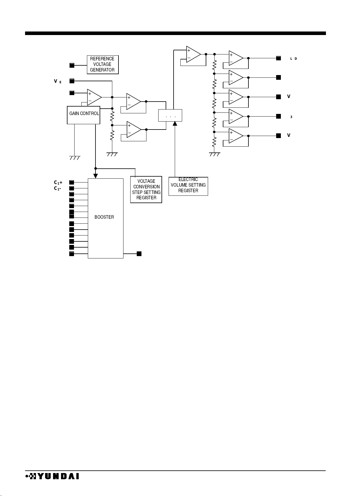
■
POWER CIRCUIT BLOCK DIAGRAM
VBA
V
REF
V
OUT
VEE
C1+
C1-
C2+
C2-
C3+
C3-
C
4
+
C4-
C5+
C5-
C6+
C6-
V W V W V
E.V.R.
V
REG
V
V W V W V W V
V1
V2
V3
V4
V
LCD
V
R
D
U
D
D
W
D
W
W
HM17CM256
- 10 -
■
PIN DESCRIPTION 1
No.
NAME
I/O
FUNCTION
21,22,23,
39,40,41
VDD
supply
Power pin for logic
27,28,29,
58,59,60
VSS
supply
GND pin for logic
67,68,69,
88,89,90
V
SSH
supply
High voltage GND pin
31
V
DDA
supply
This pin is internally connected to VDD pin.
This pin is used when the voltage of each input pin is fixed to
VDD level.
caution) Do not use to main power pin.
17,18,19,
34,35,36
V
SSA
supply
This pin is internally connected to VSS pin.
This pin is used when the voltage of each input pin is fixed to
VSS level.
caution) Do not use to main power pin.
70,71,115,116
72,73
74,75
76,77
78,79
V
LCD
V1
V2
V3
V4
supply/O
LCD driver supply voltage
•
LCD driver power supply port when external power supply
is used. When external power is used, voltages should
have following relations.
VSS<V4<V3<V2<V1<V
LCD
•
V
LCD
, V1~V4 voltages are generated by voltage booster at
master mode operation under power circuit ON.
•
When internal power supply is used, capacitors must be
connected between V
LCD
, V1~V4 and VSS.
91,92
93,94
C1+
C1-
O
Capacitor connection pin for voltage converter
95,96
97,98
C2+
C2-
O
Capacitor connection pin for voltage converter
99,100
101,102
C3+
C3-
O
Capacitor connection pin for voltage converter
103,104
105,106
C4+
C4-
O
Capacitor connection pin for voltage converter
107,108
109,110
C5+
C5-
O
Capacitor connection pin for voltage converter
111,112
113,114
C6+
C6-
O
Capacitor connection pin for voltage converter
82,83
VBA
O
Reference voltage output pin for voltage regulating.
84
V
REF
I
Reference voltage input pin for voltage regulating.
85,86,87
VEE
supply
Voltage supply pin for boosted voltage generation.
VDD level at normal status.
117,118
V
OUT
supply/O
Internal DC/DC converter output pin.
80,81
V
REG
O
Voltage regulator output pin.
24
RES
I
Reset pin
Reset when RES= “L”
HM17CM256
- 11 -
■
PIN DESCRIPTION 2
No.
NAME
I/O
FUNCTION
42
D0/SCL
I/O
43
D1/SDA
I/O
44
D2/EXCS
I/O
45
D3/SMODE
I/O
46
D4/SPOL
I/O
47,48,49
D5,D6,D7
I/O
•
When parallel interface is selected (P/S=”H”), data line is
connected to MPU data bus with 8bit bi-directional bus
•
When serial interface is selected (P/S=”L”),
D0 and D1(SCL, SDA) are used as serial interface pins
and various sets are taken by serial interface use mode of
D2, D3, D4.
SDA : serial data input pin
SCL : data transfer clock
EXCS : extension chip selection I/O pin
SMODE : serial transfer mode setting input pin
SPOL : RS polarity selection pin when 3 line serial interface is
selected.
SDA data is shifted at the rising edge of SCL
Internal serial/parallel conversion into 8-bit data occurs at the
rising edge of 8th clock of SCL.
Set to “L” after data transfer or during non-access time
50,51,52,53
54,55,56,57
D8,D9,D10,D11,
D12,D13,D14,D15
I/O
Connect to data bus to MPU with 8bit bi-directional bus.
Used as MSB 8bit data bus in the 16bit data RAM transfer
mode
Set to “L” or “H” when not used.
25
CS
I
Chip selection pin.
Data in-out is possible when CS = “L”.
Input data selection pin.
Distinguish bus data from CPU whether instruction or display
data.
RS H L
class
instruction
display data
26
RS
I
38
RD (E)
I
<80 series CPU interface (P/S=”H”,SEL68=”L”)>
RD signal connection port of 80 series CPU.
Data bus goes to output state at RD = “L”.
<68 series CPU interface (P/S=”H”,SEL68=”H”)>
Enable signal connection port of 68 series CPU.
Active status when this signal is at “H”.
<80 series CPU interface (P/S=”H”,SEL68=”L”)>
WR signal connection port of 80 series CPU.
Active at “L” and data bus signal is taken at the rising edge
of WR.
<68 series CPU interface (P/S=”H”,SEL68=”H”)>
Read write control signal , R/W connection port of 68-
series MPU.
R/W
H
L
status
read
write
37
WR (R/W)
I
HM17CM256
- 12 -
■
PIN DESCRIPTION 3
No.
NAME
I/O
FUNCTION
CPU interface selection port
SEL68
H
L
status
68 series
80 series
33
SEL68
I
Serial / parallel interface selection port
P/S
chip
select
data/
command
data
read/
write
serial clock
H
CS
RS
D0~D7
RD, WR
-
L
CS
RS
SDA(D1)
write only
SCL (D0)
32
P/S
I
P/S = “L” :serial interface selection ,D15~D5 goes to Hi-Z
state. Fix RD, WR to “H” or “L”.
20
TEST
I
Test port.
Fix to ”L”.
Latching signal pin of display data.
Display line counter is counted up at the rising edge and LCD
driving signal is generated at the falling edge
M/S
status
CL
H
master
output
L
slave
input
61
CL
I/O
LCD synchronous signal (first line marker) I/O pin.
Display start address is loaded in the display line counter at
FLM = “H”.
M/S
status
FLM
H
master
output
L
slave
input
62
FLM
I/O
Alternated display signal of LCD driver output I/O pin.
M/S
status
FR
H
master
output
L
slave
input
63
FR
I/O
Master / slave mode selection pin
M/S
mode
oscillator
Power supply
H
master
enable
enable
L
slave
disable
disable
30
M/S
I
Fix to “H” or “L” according to operating mode.
X
HM17CM256
- 13 -
PIN DESCRIPTION 4
No.
NAME
I/O
FUNCTION
Segment drive port
Segment output from display RAM data
mode
Non-lighted
lighted
Normal
0
1
Reverse
1
0
The output level is selected among V
LCD
, V2, V3, VSS by the
combination of FR signal and RAM data
(B/W mode)
FR signal
display RAM data
Normal mode
V2
V
LCD
V3
VSS
Reverse mode
V
LCD
V2
VSS
V3
174~557
SEGA0~SEGA
127
,
SEGB0~SEGB
127
,
SEGC0~SEGC
127
O
164~169,
562~567
SEGSA0~SEGSA3,
SEGSB0~SEGSB3,
SEGSC0~SEGSC3
O
Dummy segment driver output
Located at both side of segment drivers, used for edge
display.
Common driver output
The output level is selected among V
LCD
, V1, V4 and VSS by
the combination of FR and scan data.
data
FR
Output level
H H
VSS
L H V1
H L
V
LCD
L L V4
162~137,
132~119,
568~594,
3~15
COM0~COM79
O
163
COMI0
O
Common drive output for icon display
16
COMI1
O
Common drive output for icon display
65,
66
OSC1,
OSC2
I
O
External reference clock input pin
Open when using internal oscillator clock or used as slave
device.
In this case, OSC1 goes to VSS level.
Connect external oscillating source to OSC1 port or connect
resistor between OSC1 and OSC2 when using external
oscillator.
Input / output pin for display timing clock
Output clock from master device is applied to slave chip
through CLK pin when used as master / slave mode.
M/S
mode
CLK
H master
output
L slave
input*
64
CLK
I/O
*input from master chip’s CLK output
(port No. 1,2,133,134,135,136,170,171,172,173,558,559,560,561,595,596 is dummy port.)
HM17CM256
- 14 -
■
FUNCTION DESCRIPTION
(1) CPU interface
(1-1) Selection of interface type
HM17CM256
receives data through 8 bit parallel I/O(D0~D7)
16 bit parallel I/O(D0~D15) or
divided into serial data input (SDA, SCL). Parallel or serial selection is decided by P/S pin setting.
Parallel or serial selection is possible as following table.
Reading out from internal register or RAM is not possible at serial interface mode.
TABLE
P/S
Type
CS
RS
RD
WR
SEL68
SDA
SCL
data
H
Parallel input
CS
RS
RD
WR
SEL68
D0~D7 (D0~D15)
L
Serial input
CS
RS - -
-
SDA
SCL
-
caution 1) “-” mark item : Fix to ”H” or ”L”
(1-2) Parallel input
In the parallel interface mode selected by P/S port, parallel data is transferred from the
8bit/16bit MPU through data bus. SEL68 port setting makes 80-series or 68-series interface
selection
TABLE
SEL68
CPU type
CS
RS
RD
WR
data
H
68 series CPU
CS
RS
E
R/W
D0~D7 (D0~D15)
L
80 series CPU
CS
RS
RD
WR
D0~D7 (D0~D15)
(1-3) Data identification
Combinations of RS, RD, and WR signals identify contents of 8bit data bus.
TABLE
68 series
80 series
RS
R/W
RD
WR
FUNCTION
1 1 0
1
Read out from internal register
1 0 1
0
Write in to internal register
0 1 0
1
Read display data
0 0 1
0
Write display data
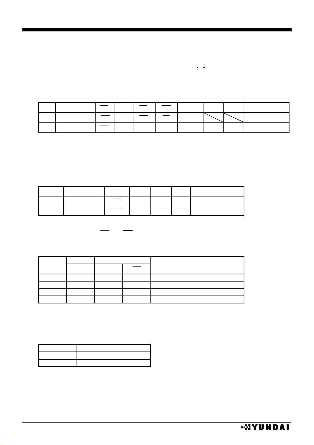
(1-4) Serial interface
2 types of serial interface (3 line type mode, 4 line type mode) are available by selecting
SMODE pin.
TABEL
SMODE
Serial interface mode
H
3 line type
L
4 line type
Y
HM17CM256
- 15 -
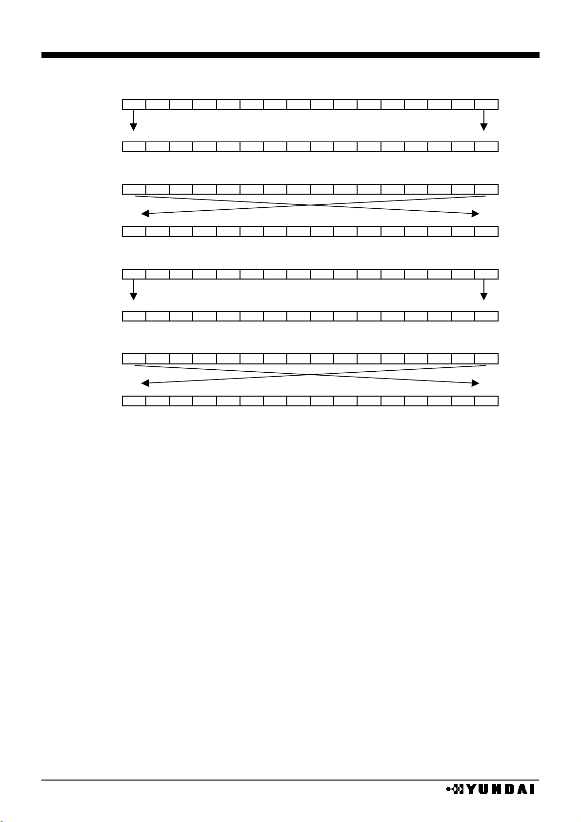
(1-5) 4 line type serial interface
4 line serial interface by SDA and SCL is possible at chip selection state (CS=”L”)
When chip is not selected, internal shift register and counter are reset to initial value.
Serial input data from SDA are latched at the rising edge of serial clock (SCL) in the sequence
of D7,
, D1, D0 and converted into 8-bit parallel data at the rising edge of 8th serial clock.
Serial data (SDA) are identified to display data or command by RS input.
TABLE
RS
Data contents
H
command
L
Display data
Make serial clock (SCL) “L” at the non-access period and after 8bit data transfer.
SDA and SCL signals are sensitive to external noise. To prevent mal-function, chip selector
state should be released (CS = “H”) after 8bit data transfer as shown in the following figure.
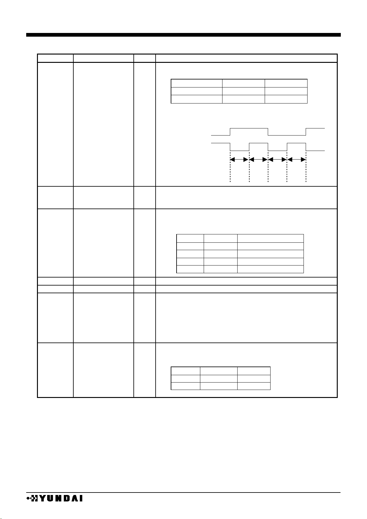
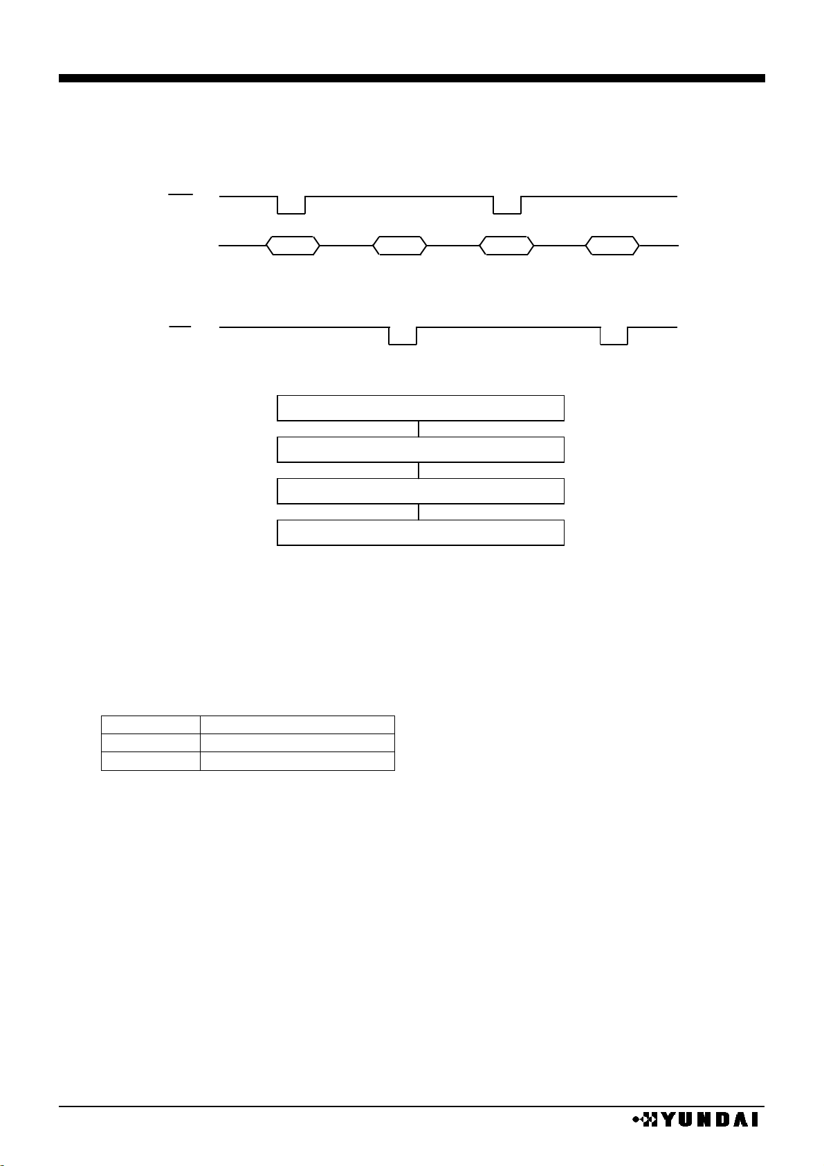
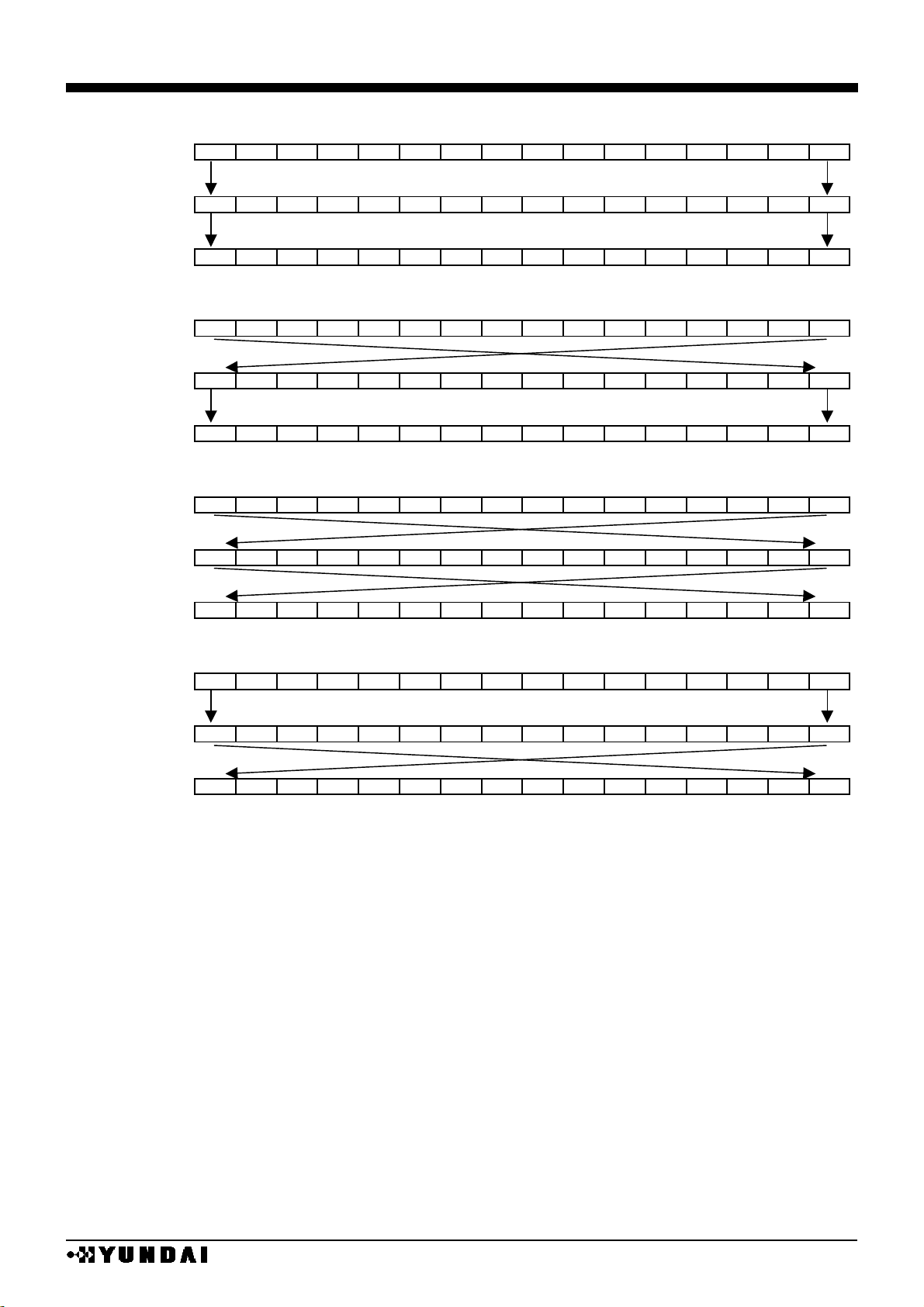
4 line serial interface
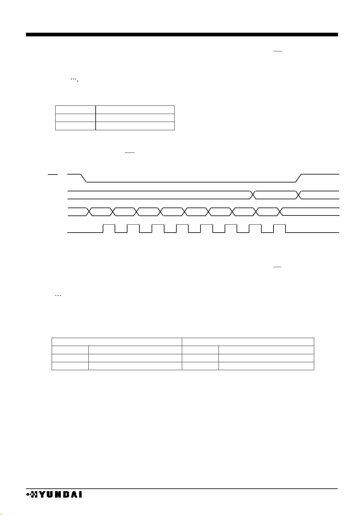
(1-6) 3 line type serial interface
3-line serial interface by SDA and SCL is possible at chip selection state (CS=”L”)
When chip is not selected, internal shift register and counter are reset to initial value.
Input data from SDA are latched at the rising edge of serial clock (SCL) in the sequence of RS,
D
7
, ,D1, D0, and converted to 8bit parallel data and handled at the rising edge of 9th serial
clock.
Serial data (SDA) are identified to display data or command by RS bit data at the rising of first
serial clock (SCL) and state of command data bit polarity shift pin (SPOL).
TABLE
SPOL=L
SPOL=H
RS
Data identify
RS
Data identify
L
Display data
L
command
H
command
H
Display data
D7
D6
D5
D4
D3
D2
D1
D0
VALID
1 2 3 4 5 6 7
8
CS
RS
SDA
SCL
Z
[
HM17CM256
- 16 -
Serial clock (SCL) should go to “L” at the non-access period and after 9bit data transfer.
SDA and SCL signals are sensitive to external noise. To prevent miss operation chip
selector state should be released (CS = “H”) after 9bit data transfer as shown in the following
figure
.
3line serial interface
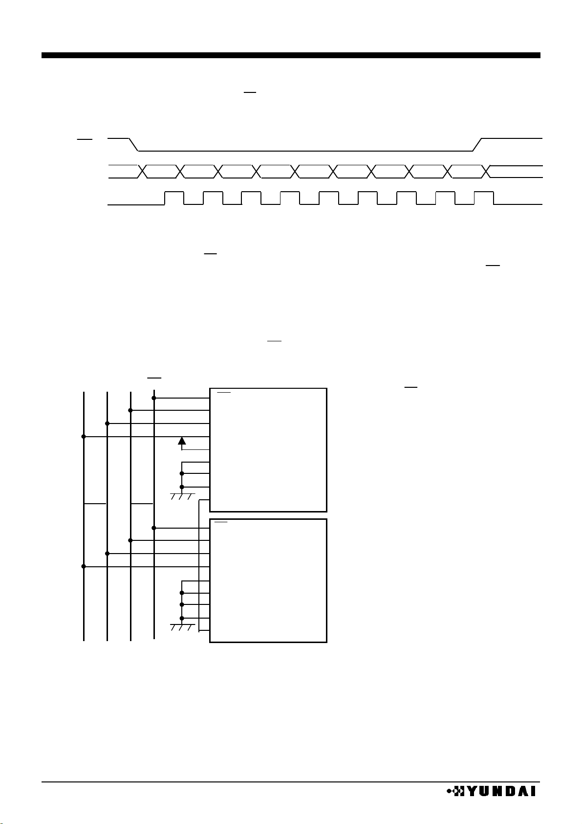
(1-7) One systematization of CS when serial interface is selected
In the multi-chip operation (master/slave) mode with serial I/F connection, one CS signal
controls two chips to reduce control signal.
Connect extended chip selection port (EXCS) of master chip to EXCS port ( input at slave
device and output at master device mode ) of slave chip.
When EXCS is “L”, master chip cannot accept command except for EXCS control; at this
point, only slave chip can be controlled.
Slave device control is possible when CS = “L” period within EXCS = “L” state.
RS
D7
D6
D5
D4
D3
D2
D1 1 2 3 4 5 6 7 8
CS
SDA
SCL
D0
9
SDA
CS
SCL
RS
M/S
P/S
SMODE
SPOL
EXCS
(MASTER)
SDA
CS
SCL
RS
M/S
P/S
SMODE
SPOL
EXCS
(SLAVE)
CS
SDA
SCL
RS
EXCS: expand CS signal ( input port )
Master device : output port
Slave device : input port
(input port)
P/S=0: serial I/F
P/S=1: parallel I/F
P/S: parallel . serial selection port
(input port)
M/S=0: slave operation
M/S=1: master operation
M/S: master . slave selection port
(input port)
SMODE=0: 4 line serial I/F
SMODE=1: 3 line serial I/F
SMODE: serial I/Fmode selection port
(input port)
Access display RAM at SPOL=0:RS=0
Access display RAM at SPOL=1:RS=1
SPOL:command data bit polarity selection port
At 3 line serial I/F mode
HM17CM256
- 17 -
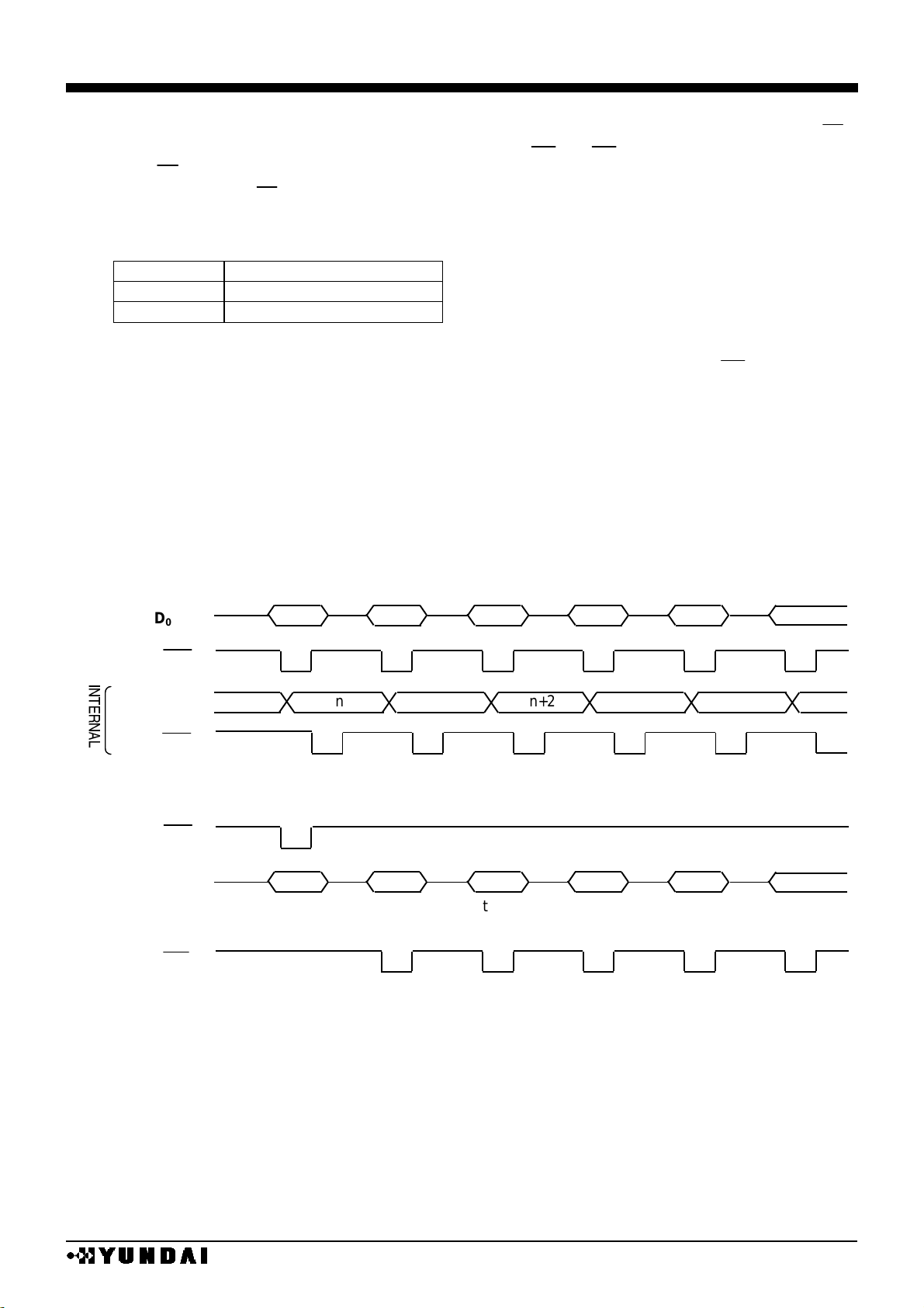
(2) DDRAM and internal register access
DDRAM and internal register are accessed by data bus D0~D7(D0~D15), chip select pin (CS),
DDRAM / register select pin (RS), read / write control pin (RD) or WR pin.
When CS=“H”, it is in non-selective state and DDRAM and internal register access is impossible.
During access, Set CS=“L”.
Access selection to DDRAM or internal register is controlled by RS input.
TABLE
RS
Data contents
L
Display RAM data
H
Internal command register
Write process starts after address setting and then the data on the 8bit data bus D0~D
7
or 16bit
data bus D0~D15 will be written in by CPU. The data is written at the rising edge of WR (80 series) or
falling edge of E (68 series).
Internally, bus holder data is processed to data bus and data are written to bus holder from CPU
until next cycle.
After address setting, data of assigned address are read at the 1st and 3rd clock, which means it
needs dummy read at the 2nd clock.
There are rules at reading data out of display RAM, after address setting, the data of assigned
address is shown directly after the end of the read command, so pay attention that assigned data is
available at 2nd timing step.
In other words, 1 cycle dummy read is needed after address setting and write cycle.
DATA WRITE IN OPERATION
DATA READ OUT OPERATION
caution) When 16 bit mode, do write in and read out by 16 bit not only RAM access but also command
setting.
n
n+2
D0~D15
WR
BUS HOLDER
WR
n
n+1
n+2
n+3
n+4
n+1
n+3
n+4
D0~D7(D0~D15)
RD
n n n+1
n+2
WR
address set
n
dummy
read
data read
n address
data read
n+1 address
data read
n+2 address
\]^
_`
]a
b
HM17CM256
- 18 -
(3) Read out of internal register
Read out is possible not only from DDRAM, but also from the internal register. Addresses for
read (0~FH) are allocated in each register.
Read out is executed after writing read-out register address to internal register.
Internal register read out sequence
When register is read out, upper 4 bit data are “1111”.
Non-used bits of active registers are “0”.
When non-used registers are read out, upper 4 bits are “1111” and lower 4 bits are “0000”.
(4) 16 bit data access to DDRAM
It is possible to write in DDRAM by 16-bits access with the data of 16 bits data bus D0~D15.
16 bits data access mode is possible by setting the value of WLS register to “1”.
TABEL
WLS
Acess mode
L
8 bit
H
16 bit
Each command should be set to 8-bits(D0~D7) as well as to 16-bit access mode.
16-bit access is available at display RAM access.
(5) Display start line register
When displaying the DDRAM data, it is the contents of Y address register that is corresponding to
display start line.
The data of Y address is displayed on the display start line depending on the value of the shift
command register and the display start line register.
The data of this register are preset to the display line counter per FLM signal transition.
Line counter is counted up in synchronization with CL input and generates line address that read
out 384bit data from DDRAM to LCD driver circuit.
D0~D7
M
N
WR
Address set
for
register read
Internal
register read
Address set
for
register read
Internal
register read
m
n
RD
RE register set:100
Internal register read address set
set RE of register to be read out
Internal register read
HM17CM256
- 19 -
(6) DDRAM addressing
This IC includes display memory Bit mapped that is composed of 1024 bit of X direction
(8bit×128) and 82bit of Y direction.
In gray mode, neighboring 3-bit data or 2-bit data are displayed by segment driver with 8 grays or
4 grays, respectively.
3 outputs of segment driver compose 1 pixel of RGB and 128×82 pixels are displayed with 256
color (8gray×8gray×4gray).
Address area of X direction is varied according to accessed data length. The area of X direction
is 0H~7FH at 8bit access mode and 0H~3FH at 16bit access mode.
•
8BIT access
X-address
0H
1H 7EH
7FH
0 H
8bit
8bit 8bit
8bit
Y-address
51H
8bit
8bit 8bit
8bit
•
16 BIT access
X-address
0H
3FH
0 H
16bit
16bit
Y-address
51H
16bit
16bit
In the Black & white mode, the MSBs of 3 bit and 2 bit corresponding with RGB are used to
display data. And so, 128x82 dot gray display or 384 x 82 B/W mode display is possible.
Display RAM is accessed with X address and Y address from CPU by 8 bit or 16 bit unit.
X address and Y address can be increased automatically by setting status of control register.
The address is increased per every read and write of display RAM by CPU. ( Please see detail
description at command function.)
X direction is selected by X address and Y direction is selected by Y address. Please do not set
the address on non-effective area and it is forbidden to set address on outside area in each case.
384bit display data of Y direction are read out to display latch at rising edge of CL signal per 1 line
cycle and this data comes out from display latch at falling edge of CL signal.
Display start line address register is preset to line counter at “H” state of FLM signal which changes
per one frame cycle and the address is counted up with synchronized CL input.
Display line address counter is synchronized by timing signals of LCD driver, and it operates
independently with X, Y address counters.
HM17CM256
- 20 -
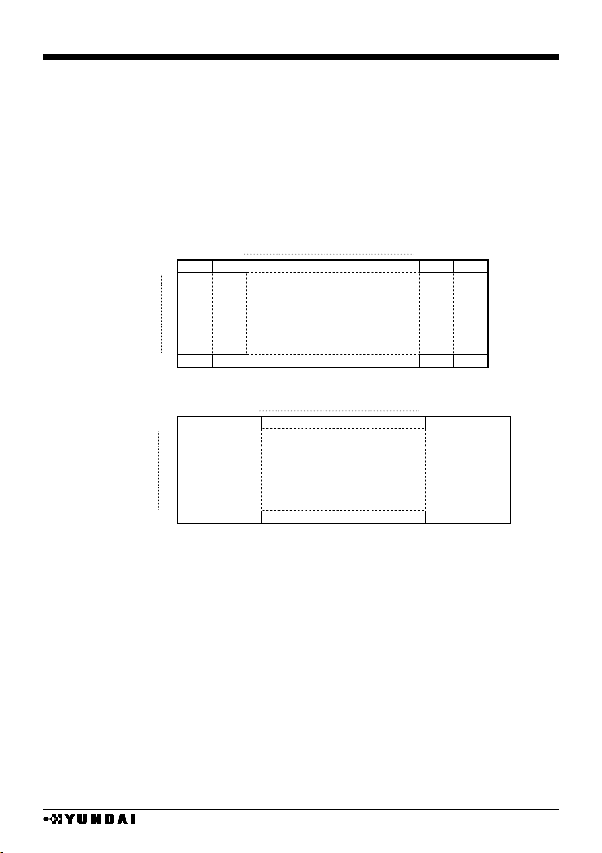
(7) Window address assign of display RAM
This IC can be accessed to display RAM by window area designation in addition to access to
display RAM designated by X and Y address.
Through address space of all display address, specific area of RAM can be accessed by
designated two points.
The start point of two point addresses is assigned by normal X address and Y address register and
the end point of them is done by X end address and Y end address register value. Designated
inner addresses depend on WLS bit.
Read modified write action can be taken by AIM=“1”.
In case of using window area accessing mode, you must set start point X address, Y address in
sequence and end point X address, Y address in sequence after executing Win command (WIN=“1”,
auto increase mode AXI=“1”, AYI=“1”) and then access to Display RAM.
And set start point and end point not to be designated to access the outside of available address
area. Address set value should be taken to set AX ≤ EX ( end point of X address ) and AY≤EY
( end point of Y address ).
X direction
(X, Y)
address designation
end address designation
Window display area
(X, Y)
All display RAM area
(8) display RAM data and LCD
Display RAM data related with one dot of LCD is dependent on REV register. Normal display and
reverse display by REV register are set up as follows.
TABLE
REV
Display
RAM data
0
L
normal
1
0
H
reverse
1
(9) Segment display output order/reverse set up
The order of display outputs, SEGA0, SEGB0, SEGC0 to SEGA
127
, SEGB
127
, and can be reversed
by reversing access to display RAM from MPU by using REF register, lessen the limitation in placing
IC when assembling an LCD panel module.
Y direction
HM17CM256
- 21 -
(10) Relation between Display RAM and address
•
RAM address and bitmap
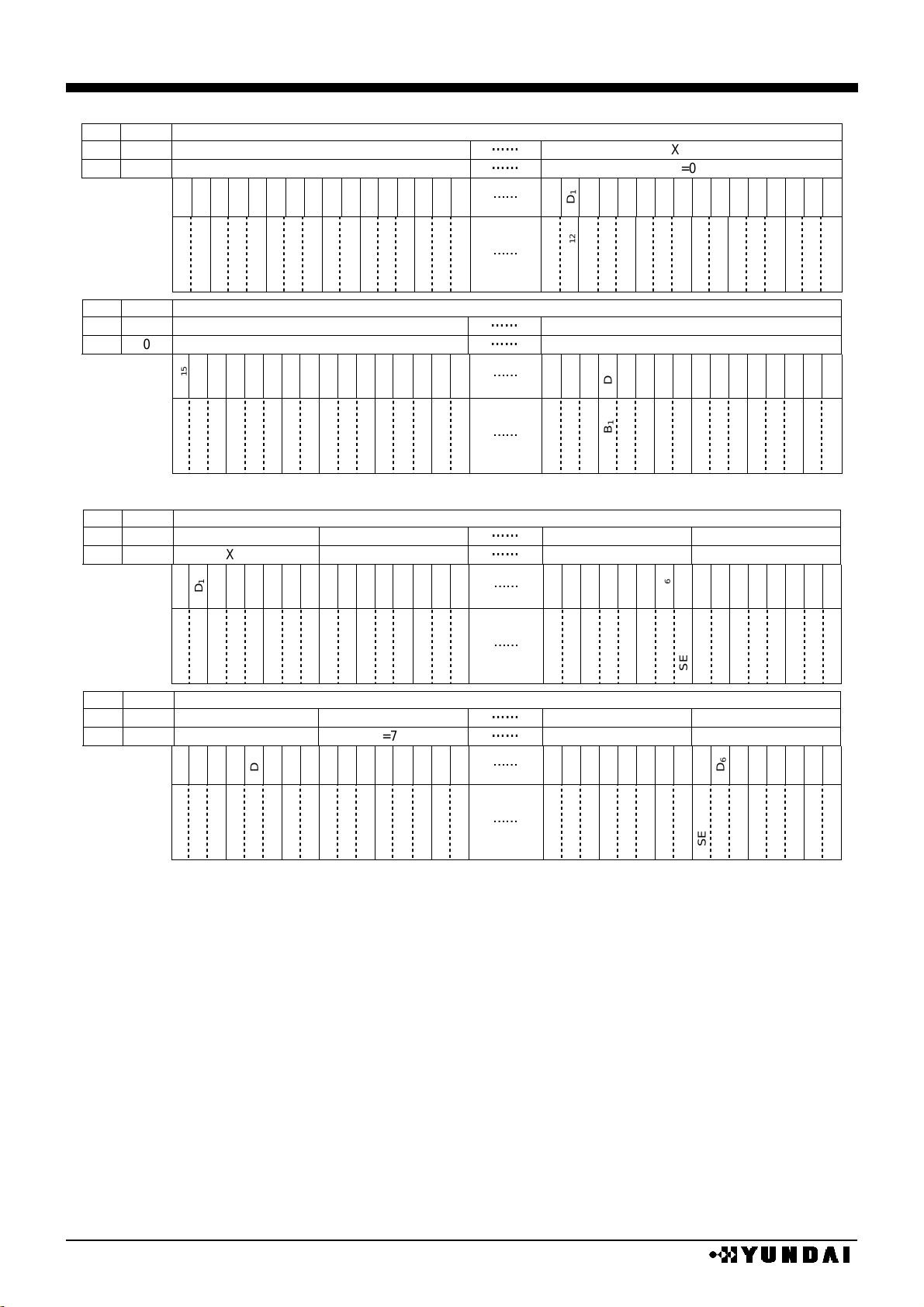
COLOR / 16 BIT MODE
REF
SWAP
X address / bit / segment assign
0
0
X=00H
X=3FH
1
1
X=3FH
X=00H
D
0
D
1
D
2
D
3
D
4
D
5
D
6
D
7
D
8
D
9
D
10
D
11
D
12
D
13
D
14
D
15
D
0
D
1
D
2
D
3
D
4
D
5
D
6
D
7
D
8
D
9
D
10
D
11
D
12
D
13
D
14
D
15
palette
A
palette B palette
C
palette
A
palette B palette
C
palette
A
palette B palette
C
palette
A
palette B palette
C
SEGA0
SEGB0
SEGC0
SEGA1
SEGB1
SEGC1
SEGA126
SEGB126
SEGC126
SEGA127
SEGB127
SEGC127
REF
SWAP
X address / bit / segment assign
0
1
X=00H
X=3FH
1
0
X=3FH
X=00H
D
15
D
14
D
13
D
12
D
11
D
10
D
9
D
8
D
7
D
6
D
5
D
4
D
3
D
2
D
1
D
0
D
15
D
14
D
13
D
12
D
11
D
10
D
9
D
8
D
7
D
6
D
5
D
4
D
3
D
2
D
1
D
0
palette C palette
B
palette
A
palette C palette
B
palette
A
palette C palette
B
palette
A
palette C palette
B
palette
A
SEGA
0
SEGB
0
SEGC
0
SEGA
1
SEGB
1
SEGC
1
SEGA
126
SEGB
126
SEGC
126
SEGA
127
SEGB
127
SEGC
127
COLOR / 8 BIT MODE
REF
SWAP
X address / bit / segment assign
0 0 X=00H
X=01H
X=7EH
X=7FH
1 1 X=7FH
X=7EH
X=01H
X=00H
D
0
D
1
D
2
D
3
D
4
D
5
D
6
D
7
D
0
D
1
D
2
D
3
D
4
D
5
D
6
D
7
D
0
D
1
D
2
D
3
D
4
D
5
D
6
D
7
D
0
D
1
D
2
D
3
D
4
D
5
D
6
D
7
palette
A
palette B palette
C
palette
A
palette B palette
C
palette
A
palette B palette
C
palette
A
palette B palette
C
SEGA
0
SEGB
0
SEGC
0
SEGA
1
SEGB
1
SEGC
1
SEGA
126
SEGB
126
SEGC
126
SEGA
127
SEGB
127
SEGC
127
REF
SWAP
X address / bit / segment assign
0 1 X=00H
X=01H
X=7EH
X=7FH
1 0 X=7FH
X=7EH
X=01H
X=00H
D
7
D
6
D
5
D
4
D
3
D
2
D
1
D
0
D
7
D
6
D
5
D
4
D
3
D
2
D
1
D
0
D
7
D
6
D
5
D
4
D
3
D
2
D
1
D
0
D
7
D
6
D
5
D
4
D
3
D
2
D
1
D
0
palette C palette
B
palette
A
palette C palette
B
palette
A
palette C palette
B
palette
A
palette C palette
B
palette
A
SEGA
0
SEGB
0
SEGC
0
SEGA
1
SEGB
1
SEGC
1
SEGA
126
SEGB
126
SEGC
126
SEGA
127
SEGB
127
SEGC
127
c c
c c
d d
d d
d d
e e
e e
d d
d d
d d
e e
e e
d d
d d
d d
e e
e e
d d
d d
d d
HM17CM256
- 22 -
BLACK & WHITE / 16 BIT MODE
REF
SWAP
X address / bit / segment assign
0
0
X=00H
X=3FH
1
1
X=3FH
X=00H
D
0
D
1
D
2
D
3
D
4
D
5
D
6
D
7
D
8
D
9
D
10
D
11
D
12
D
13
D
14
D
15
D
0
D
1
D
2
D
3
D
4
D
5
D
6
D
7
D
8
D
9
D
10
D
11
D
12
D
13
D
14
D
15
SEGA
0
SEGB
0
SEGC
0
SEGA
1
SEGB
1
SEGC
1
SEGA
126
SEGB
126
SEGC
126
SEGA
127
SEGB
127
SEGC
127
REF
SWAP
X address / bit / segment assign
0
1
X=00H
X=3FH
1
0
X=3FH
X=00H
D
15
D
14
D
13
D
12
D
11
D
10
D
9
D
8
D
7
D
6
D
5
D
4
D
3
D
2
D
1
D
0
D
15
D
14
D
13
D
12
D
11
D
10
D
9
D
8
D
7
D
6
D
5
D
4
D
3
D
2
D
1
D
0
SEGA
0
SEGB
0
SEGC
0
SEGA
1
SEGB
1
SEGC
1
SEGA
126
SEGB
126
SEGC
126
SEGA
127
SEGB
127
SEGC
127
BLACK & WHITE / 8 BIT MODE
REF
SWAP
X address / bit / segment assign
0 0 X=00H
X=01H
X=7EH
X=7FH
1 1 X=7FH
X=7EH
X=01H
X=00H
D
0
D
1
D
2
D
3
D
4
D
5
D
6
D
7
D
0
D
1
D
2
D
3
D
4
D
5
D
6
D
7
D
0
D
1
D
2
D
3
D
4
D
5
D
6
D
7
D
0
D
1
D
2
D
3
D
4
D
5
D
6
D
7
SEGA
0
SEGB
0
SEGC
0
SEGA
1
SEGB
1
SEGC
1
SEGA
126
SEGB
126
SEGC
126
SEGA
127
SEGB
127
SEGC
127
REF
SWAP
X address / bit / segment assign
0 1 X=00H
X=01H
X=7EH
X=7FH
1 0 X=7FH
X=7EH
X=01H
X=00H
D
7
D
6
D
5
D
4
D
3
D
2
D
1
D
0
D
7
D
6
D
5
D
4
D
3
D
2
D
1
D
0
D
7
D
6
D
5
D
4
D
3
D
2
D
1
D
0
D
7
D
6
D
5
D
4
D
3
D
2
D
1
D
0
SEGA
0
SEGB
0
SEGC
0
SEGA
1
SEGB
1
SEGC
1
SEGA
126
SEGB
126
SEGC
126
SEGA
127
SEGB
127
SEGC
127
f f
f f
g g
g g
f f
f f
g g
g g
f f
f f
g g
g g
f f
f f
g g
g g
HM17CM256
- 23 -
•
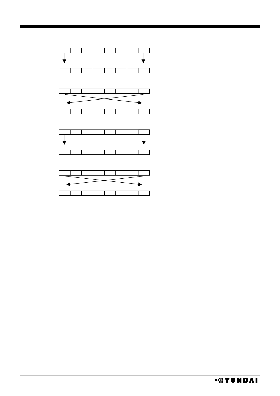
WRITE IN / READ IN BITMAP ( 16 BIT MODE )
REF=0, SWAP=0
WRITE IN DATA
D0
D1
D2
D3
D4
D5
D6
D7
D8
D9
D10
D11
D12
D13
D14
D15
SEGMENT DATA
SEG0
SEG1
SEG2
SEG3
SEG4
SEG5
SEG6
SEG7
SEG8
SEG9
SEG10
SEG11
SEG12
SEG13
SEG14
SEG15
READ IN DATA
D0
D1
D2
D3
D4
D5
D6
D7
D8
D9
D10
D11
D12
D13
D14
D15
REF=0, SWAP=1
WRITE IN DATA
D0
D1
D2
D3
D4
D5
D6
D7
D8
D9
D10
D11
D12
D13
D14
D15
SEGMENT DATA
SEG0
SEG1
SEG2
SEG3
SEG4
SEG5
SEG6
SEG7
SEG8
SEG9
SEG10
SEG11
SEG12
SEG13
SEG14
SEG15
READ IN DATA
D0
D1
D2
D3
D4
D5
D6
D7
D8
D9
D10
D11
D12
D13
D14
D15
REF=1, SWAP=0
WRITE IN DATA
D0
D1
D2
D3
D4
D5
D6
D7
D8
D9
D10
D11
D12
D13
D14
D15
SEGMENT DATA
SEG0
SEG1
SEG2
SEG3
SEG4
SEG5
SEG6
SEG7
SEG8
SEG9
SEG10
SEG11
SEG12
SEG13
SEG14
SEG15
READ IN DATA
D0
D1
D2
D3
D4
D5
D6
D7
D8
D9
D10
D11
D12
D13
D14
D15
REF=1, SWAP=1
WRITE IN DATA
D0
D1
D2
D3
D4
D5
D6
D7
D8
D9
D10
D11
D12
D13
D14
D15
SEGMENT DATA
SEG0
SEG1
SEG2
SEG3
SEG4
SEG5
SEG6
SEG7
SEG8
SEG9
SEG10
SEG11
SEG12
SEG13
SEG14
SEG15
READ IN DATA
D0
D1
D2
D3
D4
D5
D6
D7
D8
D9
D10
D11
D12
D13
D14
D15
HM17CM256
- 24 -
•
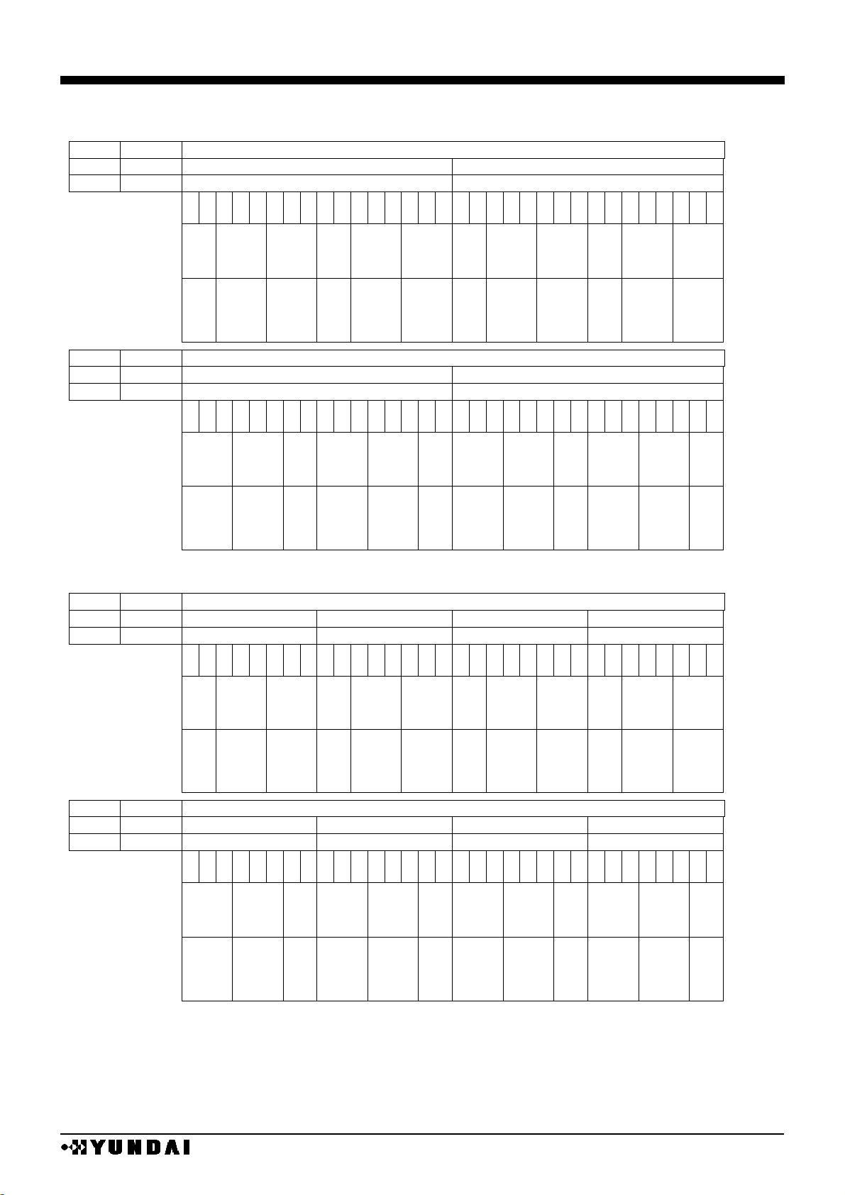
READ OUT AFTER WROTE IN DATA ( 16 BIT MODE )
REF=0, SWAP=0
D15
D0
WRITE IN DATA
1 1 1 0 0 1 0 0 1 1 1 1 0 0 1 0 (E4F2H)
D15
D0
READ IN DATA
1 1 1 0 0 1 0 0 1 1 1 1 0 0 1 0 (E4F2H)
REF=0, SWAP=1
D15
D0
WRITE IN DATA
1 1 1 0 0 1 0 0 1 1 1 1 0 0 1 0 (E4F2H)
D15
D0
READ IN DATA
0 1 0 0 1 1 1 1 0 0 1 0 0 1 1 1 (4F27H)
REF=1, SWAP=0
D15
D0
WRITE IN DATA
1 1 1 0 0 1 0 0 1 1 1 1 0 0 1 0 (E4F2H)
D15
D0
READ IN DATA
1 1 1 0 0 1 0 0 1 1 1 1 0 0 1 0 (E4F2H)
REF=1, SWAP=1
D15
D0
WRITE IN DATA
1 1 1 0 0 1 0 0 1 1 1 1 0 0 1 0 (E4F2H)
D15
D0
READ IN DATA
0 1 0 0 1 1 1 1 0 0 1 0 0 1 1 1 (4F27H)
HM17CM256
- 25 -
•
WRITE IN / READ IN BITMAP ( 8 BIT MODE )
REF=0, SWAP=0
WRITE IN DATA
D0
D1
D2
D3
D4
D5
D6
D7
SEGMENT DATA
SEG0
SEG1
SEG2
SEG3
SEG4
SEG5
SEG6
SEG7
READ IN DATA
D0
D1
D2
D3
D4
D5
D6
D7
REF=0, SWAP=1
WRITE IN DATA
D0
D1
D2
D3
D4
D5
D6
D7
SEGMENT DATA
SEG0
SEG1
SEG2
SEG3
SEG4
SEG5
SEG6
SEG7
READ IN DATA
D0
D1
D2
D3
D4
D5
D6
D7
REF=1, SWAP=0
WRITE IN DATA
D0
D1
D2
D3
D4
D5
D6
D7
SEGMENT DATA
SEG0
SEG1
SEG2
SEG3
SEG4
SEG5
SEG6
SEG7
READ IN DATA
D0
D1
D2
D3
D4
D5
D6
D7
REF=1, SWAP=1
WRITE IN DATA
D0
D1
D2
D3
D4
D5
D6
D7
SEGMENT DATA
SEG0
SEG1
SEG2
SEG3
SEG4
SEG5
SEG6
SEG7
READ IN DATA
D0
D1
D2
D3
D4
D5
D6
D7
HM17CM256
- 26 -
•
READ OUT AFTER WROTE IN DATA ( 8 BIT MODE )
REF=0, SWAP=0
D15
D0
WRITE IN DATA
1 1 1 0 0 1 0 0 (E4H)
D15
D0
READ IN DATA
1 1 1 0 0 1 0 0 (E4H)
REF=0, SWAP=1
D15
D0
WRITE IN DATA
1 1 1 0 0 1 0 0 (E4H)
D15
D0
READ IN DATA
0 0 1 0 0 1 1 1 (27H)
REF=1, SWAP=0
D15
D0
WRITE IN DATA
1 1 1 0 0 1 0 0 (E4H)
D15
D0
READ IN DATA
1 1 1 0 0 1 0 0 (E4H)
REF=1, SWAP=1
D15
D0
WRITE IN DATA
1 1 1 0 0 1 0 0 (E4H)
D15
D0
READ IN DATA
0 0 1 0 0 1 1 1 (27H)
HM17CM256
- 27 -
•
DUMMY SEGMENT REGISTER ADDRESS AND BITMAP
COLOR / 16 BIT MODE
REF
SWAP
X address / bit segment assign
0
0
X=00H
X=01H
1
1
X=01H
X=00H
D
0
D
1
D
2
D
3
D
4
D
5
D
6
D
7
D
8
D
9
D
10
D
11
D
12
D
13
D
14
D
15
D
0
D
1
D
2
D
3
D
4
D
5
D
6
D
7
D
8
D
9
D
10
D
11
D
12
D
13
D
14
D
15
Palette
A
Palette B Palette
C
Palette
A
Palette B Palette
C
Palette
A
Palette B Palette
C
Palette
A
Palette B Palette
C
SEGSA
0
SEGSB
0
SEGSC
0
SEGSA
1
SEGSB
1
SEGSC
1
SEGSA
2
SEGSB
2
SEGSC
2
SEGSA
3
SEGSB
3
SEGSC
3
REF
SWAP
X address / bit segment assign
0
1
X=00H
X=01H
1
0
X=01H
X=00H
D
15
D
14
D
13
D
12
D
11
D
10
D
9
D
8
D
7
D
6
D
5
D
4
D
3
D
2
D1
D
0
D
15
D
14
D
13
D
12
D
11
D
10
D
9
D
8
D
7
D
6
D
5
D
4
D
3
D
2
D
1
D
0
Palette C Palette
B
Palette
A
Palette C Palette
B
Palette
A
Palette C Palette
B
Palette
A
Palette C Palette
B
Palette
A
SEGSA
0
SEGSB
0
SEGSC
0
SEGSA
1
SEGSB
1
SEGSC
1
SEGSA
2
SEGSB
2
SEGSC
2
SEGSA
3
SEGSB
3
SEGSC
3
COLOR / 8 BIT MODE
REF
SWAP
X address / bit segment assign
0 0 X=00H
X=01H
X=02H
X=03H
1 1 X=03H
X=02H
X=01H
X=00H
D
0
D
1
D
2
D
3
D
4
D
5
D
6
D
7
D
0
D
1
D
2
D
3
D
4
D
5
D
6
D
7
D
0
D
1
D
2
D
3
D
4
D
5
D
6
D
7
D
0
D
1
D
2
D
3
D
4
D
5
D
6
D
7
Palette
A
Palette B Palette
C
Palette
A
Palette B Palette
C
Palette
A
Palette B Palette
C
Palette
A
Palette B Palette
C
SEGSA
0
SEGSB
0
SEGSC
0
SEGSA
1
SEGSB
1
SEGSC
1
SEGSA
2
SEGSB
2
SEGSC
2
SEGSA
3
SEGSB
3
SEGSC
3
REF
SWAP
X address / bit segment assign
0 1 X=00H
X=01H
X=02H
X=03H
1 0 X=03H
X=02H
X=01H
X=00H
D
7
D
6
D
5
D
4
D
3
D
2
D
1
D
0
D
7
D
6
D
5
D
4
D
3
D
2
D
1
D
0
D
7
D
6
D
5
D
4
D
3
D
2
D
1
D
0
D
7
D
6
D
5
D
4
D
3
D
2
D
1
D
0
Palette C Palette
B
Palette
A
Palette C Palette
B
Palette
A
Palette C Palette
B
Palette
A
Palette C Palette
B
Palette
A
SEGSA
0
SEGSB
0
SEGSC
0
SEGSA
1
SEGSB
1
SEGSC
1
SEGSA
2
SEGSB
2
SEGSC
2
SEGSA
3
SEGSB
3
SEGSC
3
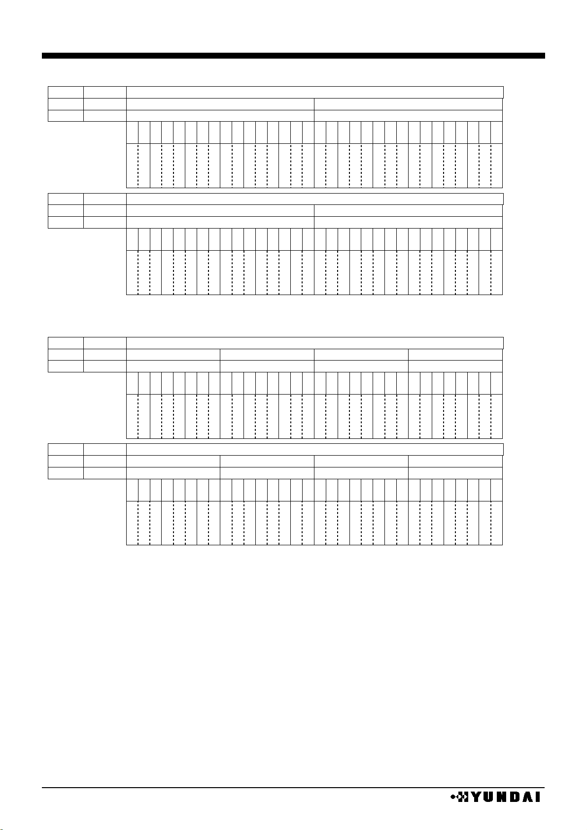
HM17CM256
- 28 -
•
BLACK 7 WHITE / 16 BIT MODE
REF
SWAP
X address / bit segment assign
0
0
X=00H
X=01H
1
1
X=01H
X=00H
D
0
D
1
D
2
D
3
D
4
D
5
D
6
D
7
D
8
D
9
D
10
D
11
D
12
D
13
D
14
D
15
D
0
D
1
D
2
D
3
D
4
D
5
D
6
D
7
D
8
D
9
D
10
D
11
D
12
D
13
D
14
D
15
SEGSA
0
SEGSB
0
SEGSC
0
SEGSA
1
SEGSB
1
SEGSC
1
SEGSA
2
SEGSB
2
SEGSC
2
SEGSA
3
SEGSB
3
SEGSC
3
REF
SWAP
X address / bit segment assign
0
1
X=00H
X=01H
1
0
X=01H
X=00H
D
15
D
14
D
13
D
12
D
11
D
10
D
9
D
8
D
7
D
6
D
5
D
4
D
3
D
2
D
1
D
0
D
15
D
14
D
13
D
12
D
11
D
10
D
9
D
8
D
7
D
6
D
5
D
4
D
3
D
2
D
1
D
0
SEGSA
0
SEGSB
0
SEGSC
0
SEGSA
1
SEGSB
1
SEGSC
1
SEGSA
2
SEGSB
2
SEGSC
2
SEGSA
3
SEGSB
3
SEGSC
3
•
BLACK & WHITE / 8 BIT MODE
REF
SWAP
X address / bit segment assign
0 0 X=00H
X=01H
X=02H
X=03H
1 1 X=03H
X=02H
X=01H
X=00H
D
0
D
1
D
2
D
3
D
4
D
5
D
6
D
7
D
0
D
1
D
2
D
3
D
4
D
5
D
6
D
7
D
0
D
1
D
2
D
3
D
4
D
5
D
6
D
7
D
0
D
1
D
2
D
3
D
4
D
5
D
6
D
7
SEGSA
0
SEGSB
0
SEGSC
0
SEGSA
1
SEGSB
1
SEGSC
1
SEGSA
2
SEGSB
2
SEGSC
2
SEGSA
3
SEGSB
3
SEGSC
3
REF
SWAP
X address / bit segment assign
0 1 X=00H
X=01H
X=02H
X=03H
1 0 X=03H
X=02H
X=01H
X=00H
D
7
D
6
D
5
D
4
D
3
D
2
D
1
D
0
D
7
D
6
D
5
D
4
D
3
D
2
D
1
D
0
D
7
D
6
D
5
D
4
D
3
D
2
D
1
D
0
D
7
D
6
D
5
D
4
D
3
D
2
D
1
D
0
SEGSA
0
SEGSB
0
SEGSC
0
SEGSA
1
SEGSB
1
SEGSC
1
SEGSA
2
SEGSB
2
SEGSC
2
SEGSA
3
SEGSB
3
SEGSC
3
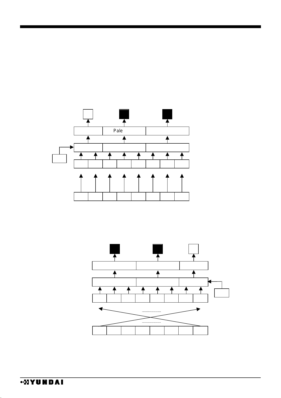
HM17CM256
- 29 -
(11) display data structure and gradation control
For the purpose of gradation control, information per pixel requires multiple bits. This IC has 3 bit
or 2 bit data per output to achieve the gradation display.
This IC is connected to an STN color LCD panel by three segment port units and one pixel consists
of three outputs of segment driver, and so 256 color ( 3 bits x 3 bits x 2 bits ) display on 128 x 82
pixels is realized.
Since one pixel data can be processed by one time access to memory, the data can be rewritten
fast and naturally.
The weight of each data bit is dependent on the status of SWAP register bit and REF register
when data is written to the display RAM.
•
ACCESS when (REF, SWAP)=(0, 0) or (1, 1)
notice) internal access X address :nH~7FH (access when REF=”0”)
:7FH~nH (access when REF=”1”)
•
ACCESS when (REF, SWAP)=(0, 1) or (1, 0)
notice) internal access X address :nH~7FH (access when REF=”0”)
:7FH~nH (access when REF=”1”)
SEGAi
SEGBi
Aj
Palette Bj
0
0
Palette Aj
1 0 0
SEGCi
Palette Cj
1 1 1
MSB
LSB
MSB
LSB
MSB
0 0 1 0 0 1 1 1 D0
D1
D2
D3
D4
D5
D6
D7 0 GLSB circuit
Gradation palette
i=0~127
j=0~7
CPU access data
X address :nH
Gradation
control circuit.
Display RAM data
SEGAi
SEGBi
1 1 1 0 0
SEGCi
Palette Aj
Palette Bj
Palette Cj
1 0 0
MSB
LSB
MSB
LSB
MSB
0 0 1 0 0 1 1 1 D0
D1
D2
D3
D4
D5
D6
D7
Gradation palette
i=0~127
j=0~7
CPU access data
X address :nH
Gradation
control circuit
Display RAM data
0
GLSB circuit
h i j k
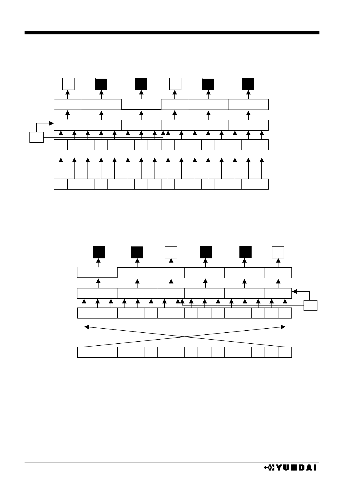
HM17CM256
- 30 -
When display RAM is accessed by 16 bit data width, the weight of each data bit is dependent on
the status of SWAP register and REF register, the same method as 8 bit access
•
ACCESS when (REF, SWAP)=(0, 0) or (1, 1)
notice) internal access X address :nH~3FH (access when REF=”0”)
:3FH~nH (access when REF=”1”)
•
ACCESS when (REF, SWAP)=(0, 1) or (1, 0)
notice) internal access X address :nH~3FH (access when REF=”0”)
:3FH~nH (access when REF=”1”)
MSB
LSB
MSB
LSB
MSB
GLSB circuit
CPU access data
X address :nH
1
LSB
MSB
LSB
MSB
MSB
1 0 0 0 0 0 1 1 1 1 0 1 1 1 1 0 0
D0
D1
D2
D3
D4
D5
D6
D7
D8
D9
D10
D11
D12
D13
D14
D15
SEGAi
SEGBi
0
Palette Aj
SEGCi
Palette Cj
Gradation palette
i=0~126
j=0~7
Gradation
control ciruit
Display RAM data
0 0 0 0 1 1 1 1 0 0 SEGBi+1
Palette Bj
Palette Cj
Palette Bj
Palette Aj
SEGAi+1
SEGCi+1
1 1 0 0 SEGAi
SEGBi
1
Palette Aj
SEGCi
Palette Cj
MSB
LSB
MSB
LSB
MSB
GLSB circuit
Gradation palette
i=0~126
j=0~7
CPU access data
X address :nH
Graydation
control ciruit
Display RAM data
1 0 0 1 1 1 0 0 1 1 0
LSB
MSB
LSB
MSB
MSB
SEGBi+1
Palette Bj
Palette Cj
Palette Bj
Palette Aj
SEGAi+1
SEGCi+1
1 0 0 0 0 0 0 0 0 1 1 1 1 0 1 1 1 1 0 0 0
D0
D1
D2
D3
D4
D5
D6
D7
D8
D9
D10
D11
D12
D13
D14
D15
 Loading...