

HEI HL15604 Datasheet
H L 1 5 6 0 4
LCD Driver IC
HL15604
Preliminary
2Q. 1999
Hyundai Electronics Industries
System IC Division
1
P r e l i m i n a r y

Contents
1. General Description
2. Features
3. Block Diagram
4. Pin Diagram
5. Pin Description
6. Serial I/O Data Format
7. Registers
HL15604
8. Key Scan Function
9. LCD Function
10. Power On Reset
11. Power Down Mode
12. Oscillator Port
13. Electrical Characteristics
14. Application
2
P r e l i m i n a r y
HL15604
1. General Description
The HL15604 is 1/3,1/4 duty LCD display driver. It can drive directly maximum
224 segments. Also it has four general purpose output ports and a key scan
function that accepts input from up to 30 keys.
2. Features
• LCD display ..................................... 56 segments x 3 commons
1/3 duty - 1/2 bias
1/3 duty - 1/3 bias
………………………….. 56 segments x 4 commons
1/4 duty - 1/3 bias
• Key scan ............................................ Maximum 30 keys
Input 5 pins, Output 6 pins
• Power down mode ............................. Sleep mode and all segments off mode
• Port
Output .................................................. 4 pins
( Including the LCD segment port )
• Serial I/O .............................................. Data transfer and receive
• Power on reset ..................................... Supply voltage detection ( SVD )
• RC oscillator
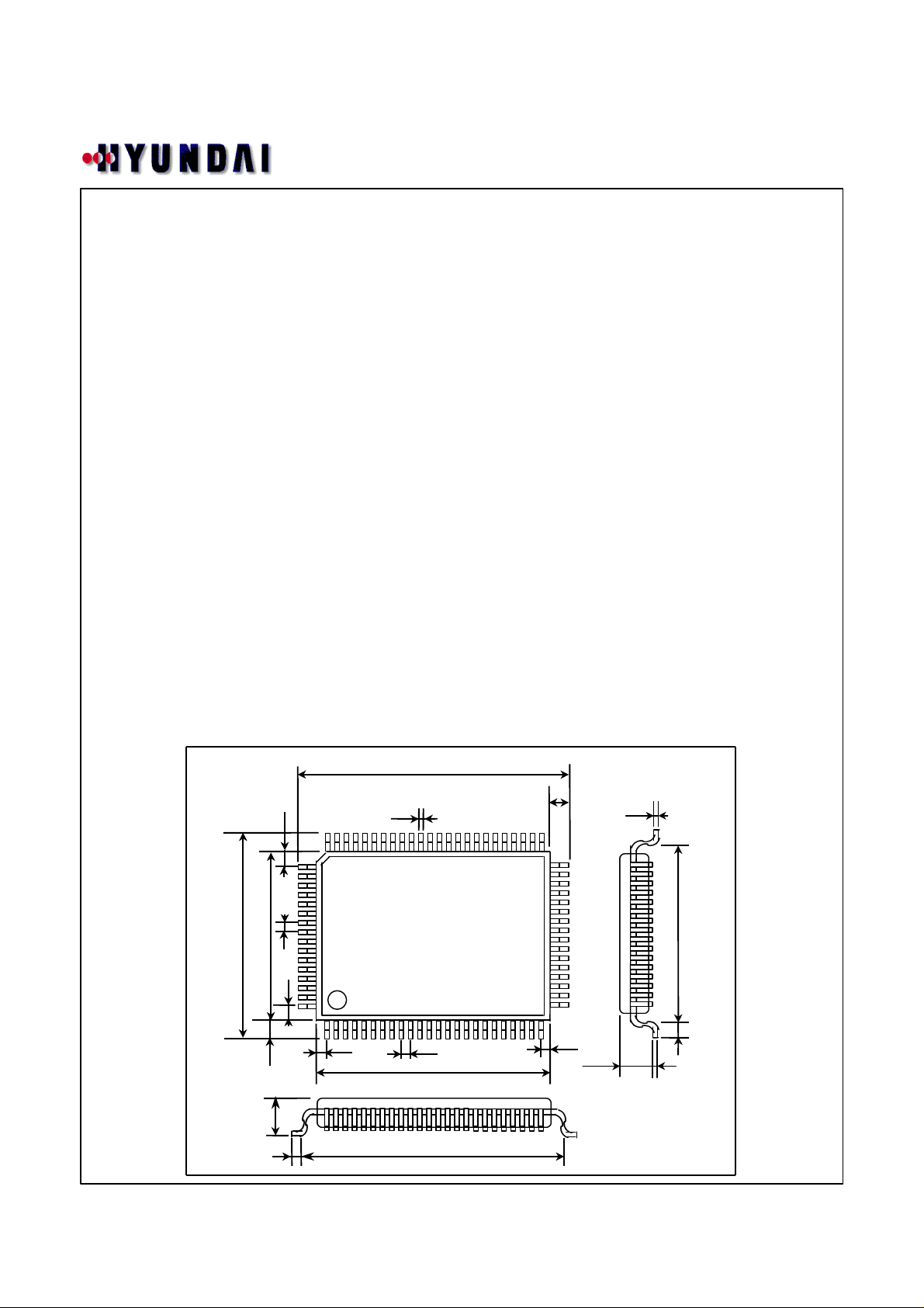
• Package ............................................... 80QFP
Package Dimensions
80QFP
17.2
14.0
1.5
3.0 max
23.2
0.35
1.0
64
65
1.0
80
1 24
20.0
21.6
3
0.5
41
40
25
0.15
2.70
15.5
0.5
0.1
Unit : mm
P r e l i m i n a r y
80QFP
14.0
12.0
1.25
0.5
1.25
61
60
1.25
0.20
14.0
12.0
0.5
1.25
41
HL15604
0.135
40
3. Block Diagram
VCL1
VCL2
VDD
VSS
RES
OSC
80
1
max
1.6
COM4
COM3
COM2
COMMOM
DRIVER
LCD
BIAS
SVD
CLOCK
GENERATOR
COM1
RESET
CLOCK
21
20
1.4
0.50.5
KS2 / SEG56
KS1 / SEG55
SEG54
SEGMENT
DRIVER
LCD
DISPLAY & CONTROL
REGISTER
SERIAL
I/O
0.1
Unit : mm
SEG5
SEG4 / P4
SEG1 / P1
SI
SO
SCK
CE
MODE
MODE
CONTROL
KS5
4
KS4
KS3
KS2
KEY
SCAN
KS1
KIN6
KIN5
KIN4
KIN3
KIN2
KIN1
P r e l i m i n a r y
4. Pin Diagram
KS6
KS5
KS4
KS3
KS2 / SEG56
KS1 / SEG55
COM4
COM3
COM2
COM1
SEG54
SEG53
SEG52
SEG51
SEG50
SEG49
SEG48
SEG47
SEG46
SEG45
SEG44
SEG43
SEG42
SEG41
HL15604
KIN1
KIN2
KIN3
KIN4
KIN5
VDD
VCL1
VCL2
VSS
MODE
OSC
RES
SO
CE
SCK
SI
64
65
70
80
1
P1 / SEG1
P2 / SEG2
60
SEG5
SEG6
SEG7
SEG8
P4 / SEG4
P3 / SEG3
KS2 / SEG56
KS1 / SEG55
COM4
COM3
COM2
50
10 20
SEG9
SEG10
SEG11
SEG12
SEG13
SEG14
SEG15
SEG16
SEG17
COM1
SEG54
SEG53
SEG52
SEG51
SEG50
SEG49
SEG48
SEG47
SEG46
SEG18
SEG19
SEG20
SEG45
SEG44
SEG43
41
24
SEG21
SEG22
SEG23
SEG42
SEG41
40
30
25
SEG24
SEG40
SEG39
SEG38
SEG37
SEG36
SEG35
SEG34
SEG33
SEG32
SEG31
SEG30
SEG29
SEG28
SEG27
SEG26
SEG25
KS3
KS4
KS5
KS6
KIN1
KIN2
KIN3
KIN4
KIN5
VDD
VCL1
VCL2
VSS
MODE
OSC
RES
SO
CE
SCK
SI
61
70
80
1
P1 / SEG1
P2 / SEG2
SEG5
SEG6
SEG7
P4 / SEG4
P3 / SEG3
5060
10 20
SEG8
SEG9
SEG10
SEG11
SEG12
SEG13
SEG14
SEG15
SEG16
5
41
40
30
21
SEG17
SEG18
SEG19
SEG40
SEG39
SEG38
SEG37
SEG36
SEG35
SEG34
SEG33
SEG32
SEG31
SEG30
SEG29
SEG28
SEG27
SEG26
SEG25
SEG24
SEG23
SEG22
SEG21
SEG20
P r e l i m i n a r y
5. Pin Description
HL15604
PIN Name I/O
SEG[56:1] O
COM [4:1] O 4 LCD Common Pins
VCL[2:1] I 2 LCD Bias Pins
OSC I/O 1 Oscillator Input Pin
KS[6:1] O 6 Key Scan Output Pins
KIN[5:1] I 5 Key Scan Input Pins
CE I 1 Serial I/O Control Pin
SCK I 1 Serial I/O Clock Pin
SO O 1 Serial I/O Data Output Pin
SI I 1 Serial I/O Data Input Pin
P[4:1] O 4 Output Port share SEG[4:1]
RES I 1 Reset Pin
MODE I 1 3 Common, 4 Common Select Pin
VDD I 1 Power Supply Pin
VSS
I
Pin Number
56
1 Ground Pin
LCD SEG Pins share P1,P2,P3 and P4
Contents
6
P r e l i m i n a r y
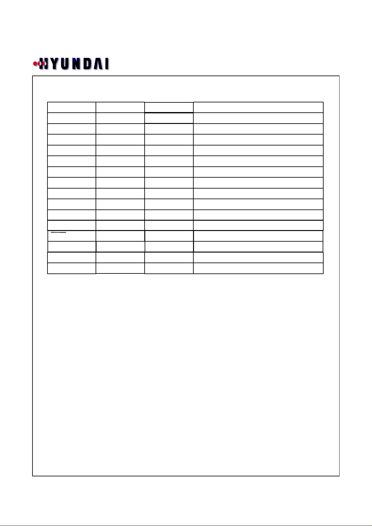
6. Serial I/O Data Format
1) 3Common Writing Mode
i )SCK is stopped at the low level
CE
SCK
HL15604
SI
SO
CE
SCK
SI
SO
B0 B1 B2 B3 A0 A1 A2 A3
B0 B1 B2 B3 A0 A1 A2 A3
0 1 0 0 0 0 1 0 D1 D2 D3XX
Display data
D56
D57 0 0 0 0 S0 S1 K0 K1 P0 P1 SC DR 0 0
0
Control data DD
D111
0 1 0 0 0 0 1 0 D57 D58 D59XX
Display data
D114
0 0 0 0 0 1
0 0 0 0 0 0
Fixed data DD
0 0 0
CE
SCK
SI
SO
XX
B0 B1 B2 B3 A0 A1 A2 A3
0 1 0 0 0 0 1 0 D115
D116 D117
Display data
D168
0
0 0 0 0 1 0
00
0 0 0 0 0 0
Fixed data DD
7
0 0 0
P r e l i m i n a r y

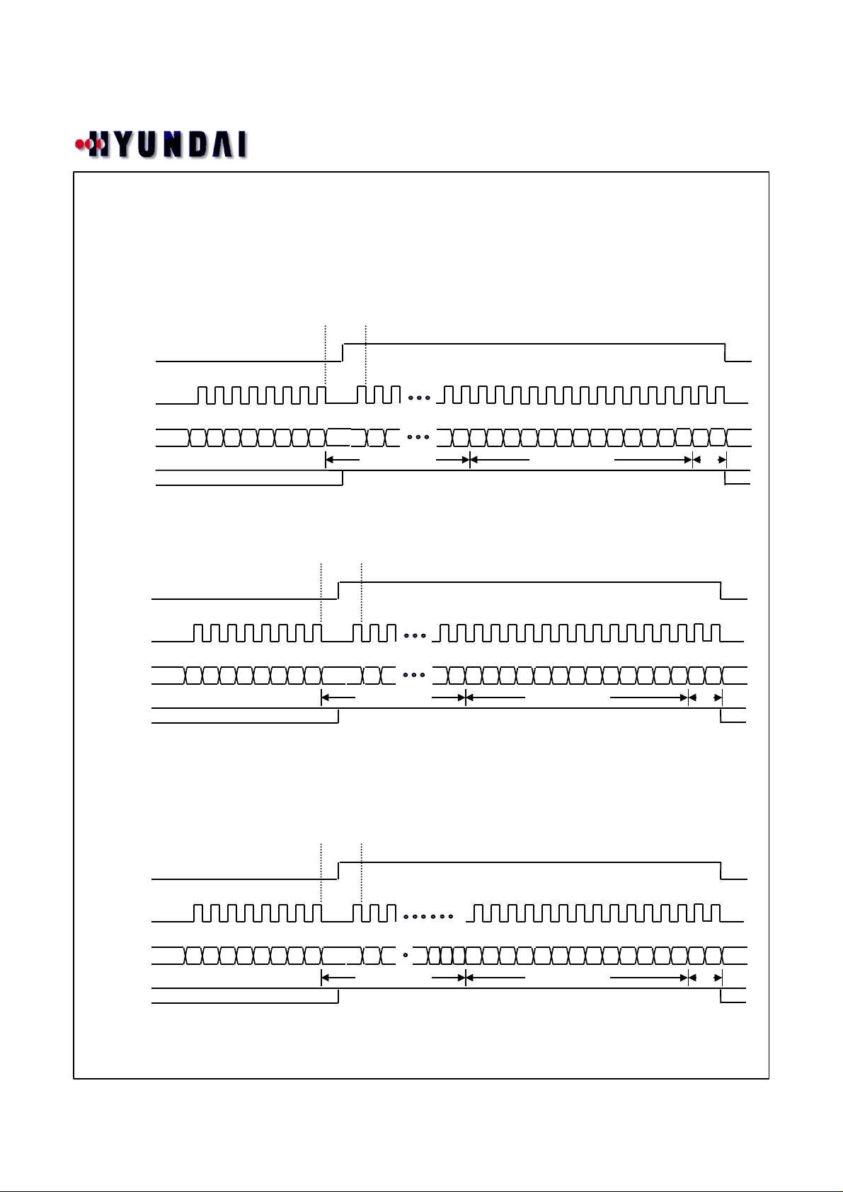
ii )SCK is stopped at the high level
CE
SCK
HL15604
SI
SO
CE
SCK
SI
SO
CE
SCK
SI
SO
B0 B1 B2 B3 A0 A1 A2 A3
B0 B1 B2 B3 A0 A1 A2 A3
XX
B0 B1 B2 B3 A0 A1 A2 A3
1 0 0 0 0 1 0 0 D2 D3XX
1 0 0 0 0 1 0 0 D59 D60XX
1 0 0 0 0 1 0 0
D1
D58
D115
Display data
Display data
D116 D117
Display data
D56
D57 0 0 0 0 S0 S1 K0 K1 P0 P1 SC DR 0 0
Control data DD
D113
D114
0 0 0 0 0
0 0 0 0
Fixed data DD
D168
0
00
0 0 0 0 1
0 0 0 0
Fixed data DD
0 0 0 0
0 0 0 0
1
0
Address : 42H
D168~D1 : Display data
S0, S1 : Sleep control data
K0, K1 : Key scan output / Segment output selection data
P0, P1 : Segment output / general-purpose output port selection data
SC : Segment on / off control data
DR : 1/2 bias or 1/3 bias drive selection data
8
P r e l i m i n a r y

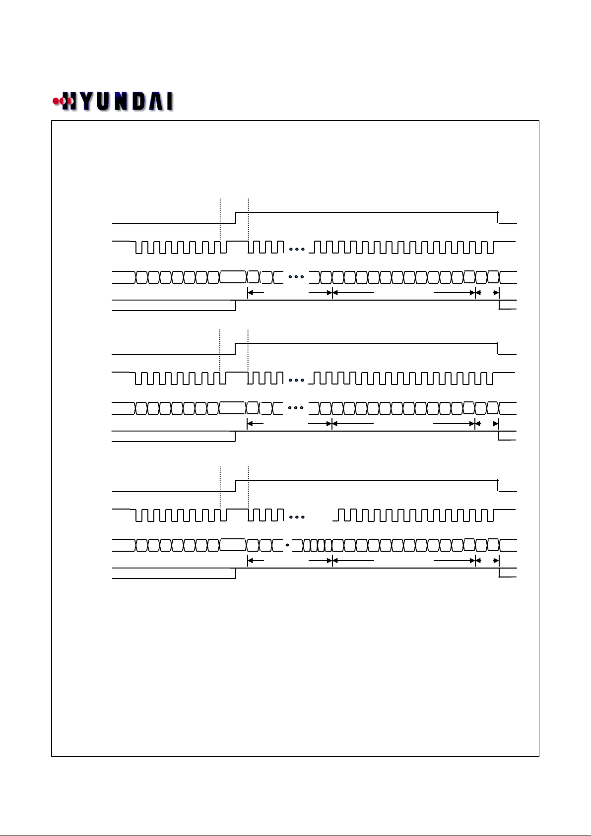
2) 4Common Writing Mode
i )SCK is stopped at the low level
CE
SCK
HL15604
SI
SO
CE
SCK
SI
SO
B0 B1 B2 B3 A0 A1 A2 A3
B0 B1 B2 B3 A0 A1 A2 A3
0 1 0 0 0 0 1 0 D1 D2 D3XX
Display data
D75
D76 0 0 0 0 S0 S1 K0 K1 P0 P1 SC DR 0 0
0
Control data DD
D151
0 1 0 0 0 0 1 0 D77 D78 D79XX
Display data
D152
0 0 0 0 0 1
0 0 0 0 0 0
Fixed data DD
0 0 0
CE
SCK
SI
SO
XX
B0 B1 B2 B3 A0 A1 A2 A3
0 1 0 0 0 0 1 0 D153
D154 D155
Display data
D224
0 0 0 0
9
0 0 0 0 1 0
0 0 0 0 0 0
Fixed data DD
0 0 0
P r e l i m i n a r y
ii )SCK is stopped at the high level
CE
SCK
HL15604
SI
SO
CE
SCK
SI
SO
CE
SCK
SI
SO
1 0 0 0 0 1 0 0 D2 D3XX
B0 B1 B2 B3 A0 A1 A2 A3
1 0 0 0 0 1 0 0 D78 D79XX
B0 B1 B2 B3 A0 A1 A2 A3
1 0 0 0 0 1 0 0XX
B0 B1 B2 B3 A0 A1 A2 A3
D1
D77
D153 D154
Display data
Display data
D155
D224
Display data
D75
D76 0 0 0 0 S0 S1 K0 K1 P0 P1 SC DR 0 0
Control data DD
D151
D152
0 0 0 0 0
0 0 0 0
Fixed data DD
0 0 0 0
0 0 0 0 1
0 0 0 0
Fixed data DD
0 0 0 0
0 0 0 0
1
0
Address : 42H
D168~D1 : Display data
S0, S1 : Sleep control data
K0, K1 : Key scan output / Segment output selection data
P0, P1 : Segment output / general-purpose output port selection data
SC : Segment on / off control data
DR : 1/2 bias or 1/3 bias drive selection data
10
P r e l i m i n a r y
 Loading...