

HEI HL15203 Datasheet
H L 1 5 2 0 3
LCD Driver IC
HL15203
Preliminary
2Q. 1999
Hyundai Electronics Industries
System IC Division
1
P r e l i m i n a r y

Contents
1. General Description
2. Features
3. Block Diagram
4. Pin Diagram
5. Pin Description
6. Serial I/O Data Format
7. Registers
HL15203
8. Key Scan Function
9. LCD Function
10. INH and Display Control
11. Power Down Mode
12. Oscillator Port
13. Electrical Characteristics
14. Application
2
P r e l i m i n a r y
HL15203
1. General Description
The HL15203 is 1/3 duty LCD display driver. It can drive directly maximum
156 segments.
2. Features
• LCD display ..................................... 52 segments x 3 commons
1/3 duty - 1/2 bias
1/3 duty - 1/3 bias
• Power down mode ..........................…. Sleep mode and all segments off mode
• Serial I/O .............................................. Data transfer and receive
• RC oscillator
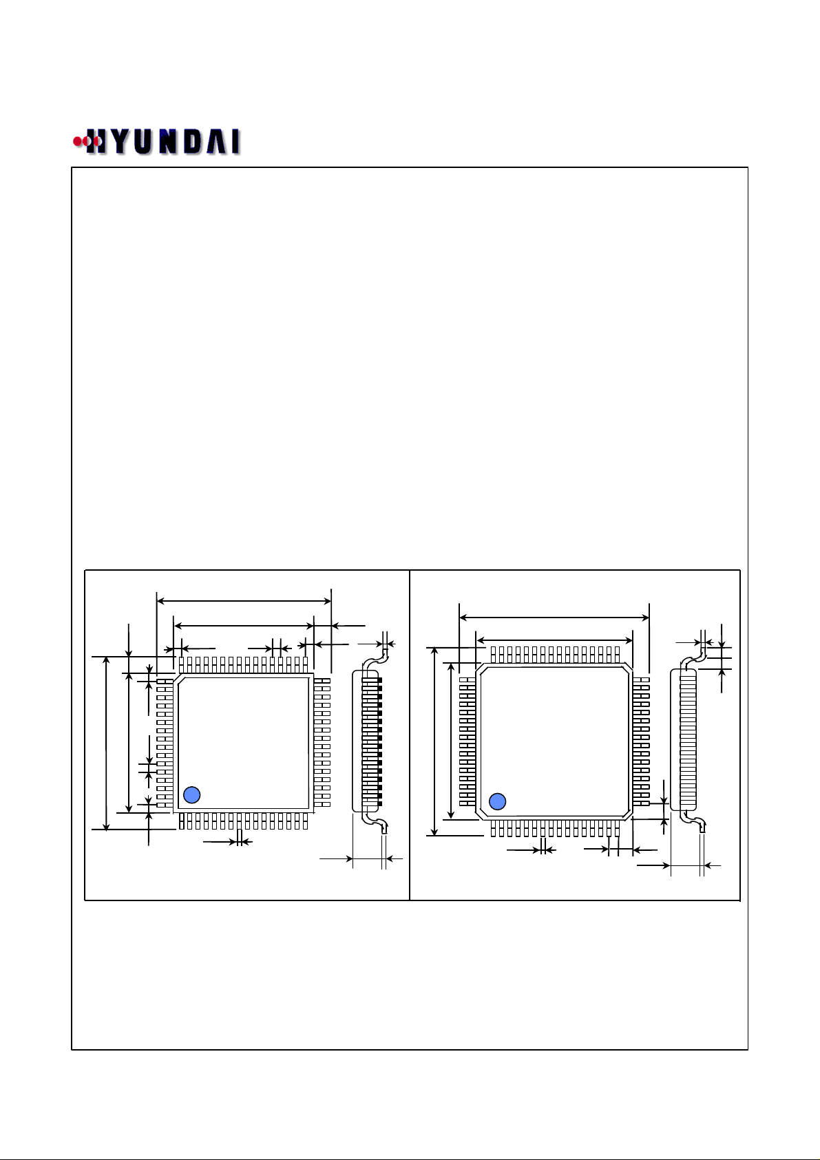
• Package ............................................... 64QFP
Package Dimensions
64QFP(14¡¿14)
1.6
49
1.0
14.0
17.2
Unit : mm
0.8
1.0
64
1
1.0
0.35
17.2
14.0
0.8
16
3348
32
17
1.0
2.70
1.6
0.15
64QFP(12¡¿12)
10.0
12.0
0.1
Unit : mm
48
49
64
12.0
10.0
1
0.35
16
0.5 1.25
1.7max
33
32
17
0.15
1.25
0.5
0.5
0.1
3
P r e l i m i n a r y
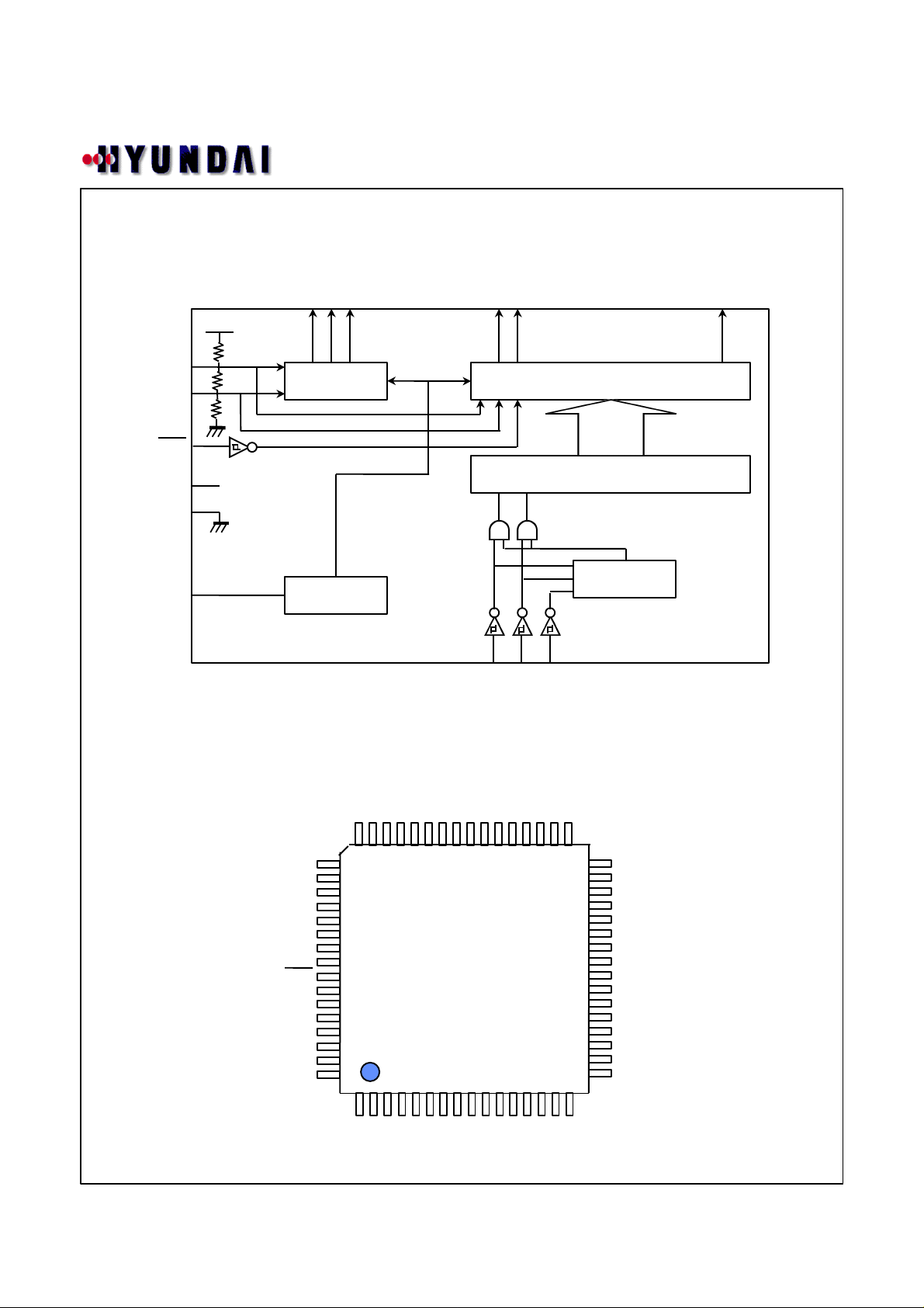
3. Block Diagram
•
COM1
COM2
COM3
...........
SEG52
SEG51
HL15203
SEG1
VCL1
VCL2
INH
VDD
VSS
OSC
•
•
4. Pin Diagram
•
•
COMMON
DRIVER
•
LATCH & DRIVER
SHIFT REGISTER
•
CLOCK
GENERATOR
•
•
SI
SCK
ADDRESS
DETECTOR
CE
SEG49
SEG50
SEG51
SEG52
COM1
COM2
COM3
VDD
INH
VCL1
VCL2
VSS
OSC
CE
SCK
SI
49
64
48
1
SEG48
SEG47
SEG46
SEG2
SEG1
SEG3
SEG45
SEG44
SEG43
SEG42
SEG41
HL15203
SEG4
SEG5
SEG6
SEG7
SEG8
4
SEG40
SEG39
SEG38
SEG9
SEG10
SEG11
SEG37
SEG36
SEG35
SEG12
SEG13
SEG14
SEG34
SEG33
33
32
17
16
SEG15
SEG16
SEG32
SEG31
SEG30
SEG29
SEG28
SEG27
SEG26
SEG25
SEG24
SEG23
SEG22
SEG21
SEG20
SEG19
SEG18
SEG17
P r e l i m i n a r y
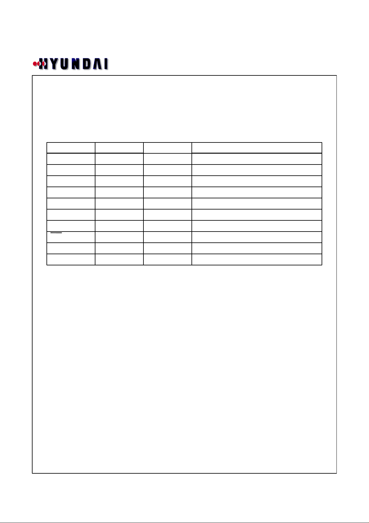
5. Pin Description
PIN Name I/O Pin Number Contents
HL15203
SEG[52:1] O
COM [3:1] O 3 LCD Common Pins
VCL[2:1] I 2 LCD Bias Pins
OSC I 1 Oscillator Input Pin
CE I 1 Serial I/O Control Pin
SCK I 1 Serial I/O Clock Pin
SI I 1 Serial I/O Data Input Pin
INH I 1 Display off control pin
VDD I 1 Power Supply Pin
VSS I 1 Ground Pin
52
LCD SEG Pins
5
P r e l i m i n a r y
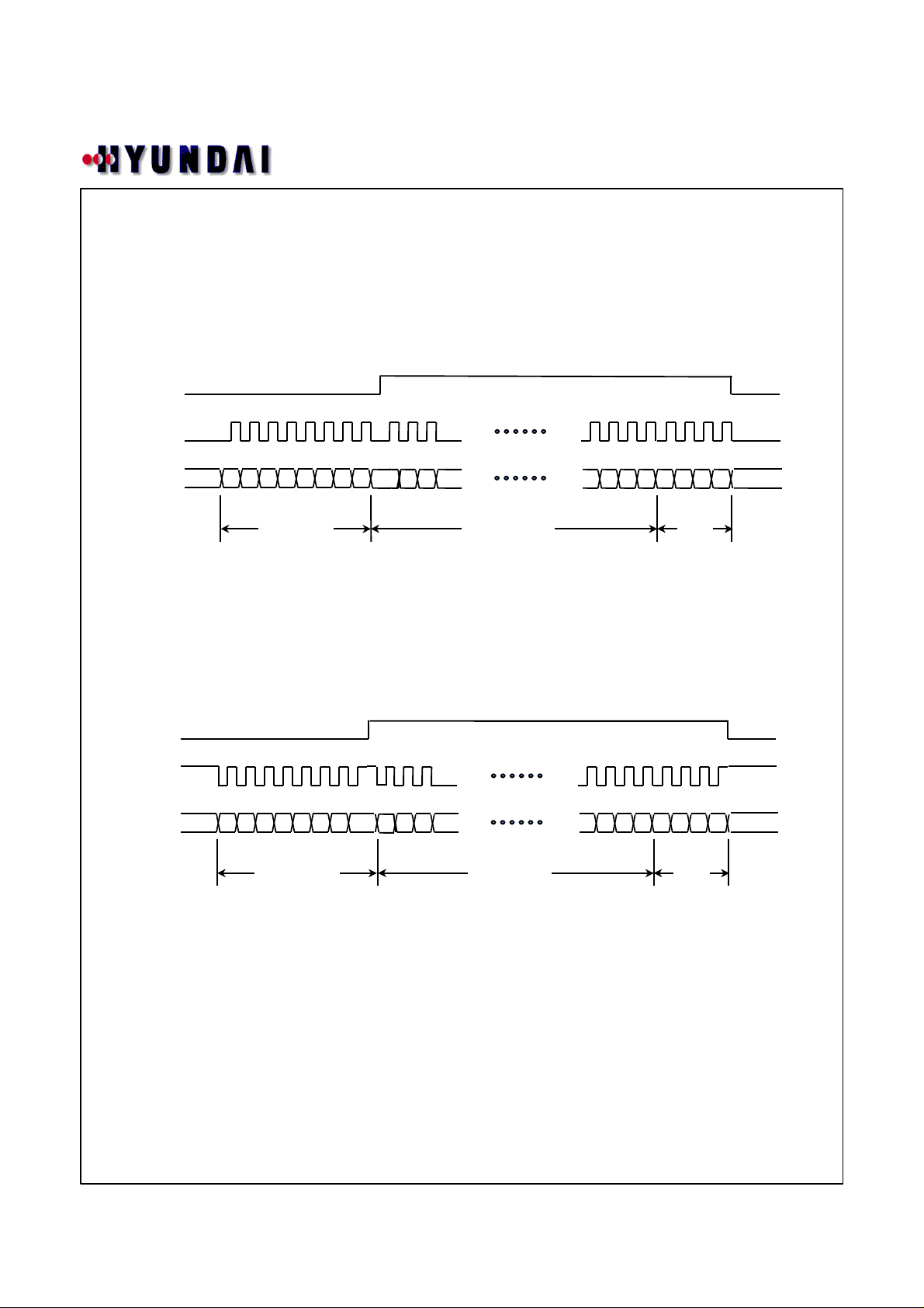
DATA Writing
i ) SCK is stopped at the low level
CE
SCK
HL15203
SI
Address
8 bits
ii ) SCK is stopped at the high level
CE
SCK
SI
Address
8 bits
D2 D3
D1
01000011XX
A7A5A3A1 A6A4A2A0
Display data
156bits
D154 D155 D156
DR
BUSC
Control data
4 bits
¡¿
0
1000001XX
A7A5A3A1 A6A4A2A0
D2 D3
D1
Display data
156bits
D154 D155 D156
DR
BUSC
Control data
4 bits
¡¿
ADDRESS : 41H
D1 ~ D156 : Display data
Dn(n=1~156)=1 ……….. Display on
Dn(n=1~156)=0 ……….. Display off
DR : 1/2-bias drive or 1/3-bias drive switching control data
SC : Segments on/off control data
BU : Normal mode/power-saving mode control data
6
P r e l i m i n a r y
 Loading...