

HEI HG74ALVC162835C Datasheet
18-BIT UNIVERSAL BUS DRIVER HG74ALVC162835C
OE
WITH 3-STATE OUTPUTS Jan. 1999
Features
l Ideal for Use in PC100 Registered DIMM
l 0.5µm CMOS Technology
l 2.3 ~ 3.6 V
Operation
CC
l Output Port Has 26-ΩSeries Damping
Resistor, No External Resistors are Required
l Package Options Include Plastic Thin Shrink
Small-Outline Packages, Shrink Small-Outline
Packages , Thin Very Small Outline Packages
(TSSOP 56 Pins, SSOP 56 Pins , TVSOP 56 Pins)
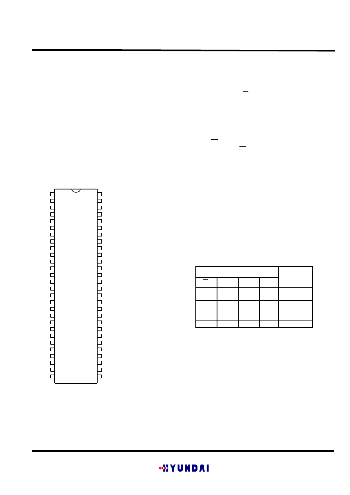
Pin Configuration
(TOP VIEW)
NC
NC
Y1
GND
Y2
Y3
Vcc
Y4
Y5
Y6
GND
Y7
Y8
Y9
Y10
Y11
Y12
GND
Y13
Y14
Y15
Vcc
Y16
Y17
GND
Y18
OE
LE
1
2
3
4
5
6
7
8
9
10
11
12
13
14
15
16
17
18
19
20
21
22
23
24
25
26
27
28
56
GND
55
NC
54
A1
53
GND
52
A2
51
A3
50
Vcc
49
A4
48
A5
47
A6
46
GND
45
A7
44
A8
43
A9
42
A10
41
A11
40
A12
39
GND
38
A13
37
A14
36
A15
35
Vcc
34
A16
33
A17
32
GND
31
A18
30
CLK
29
GND
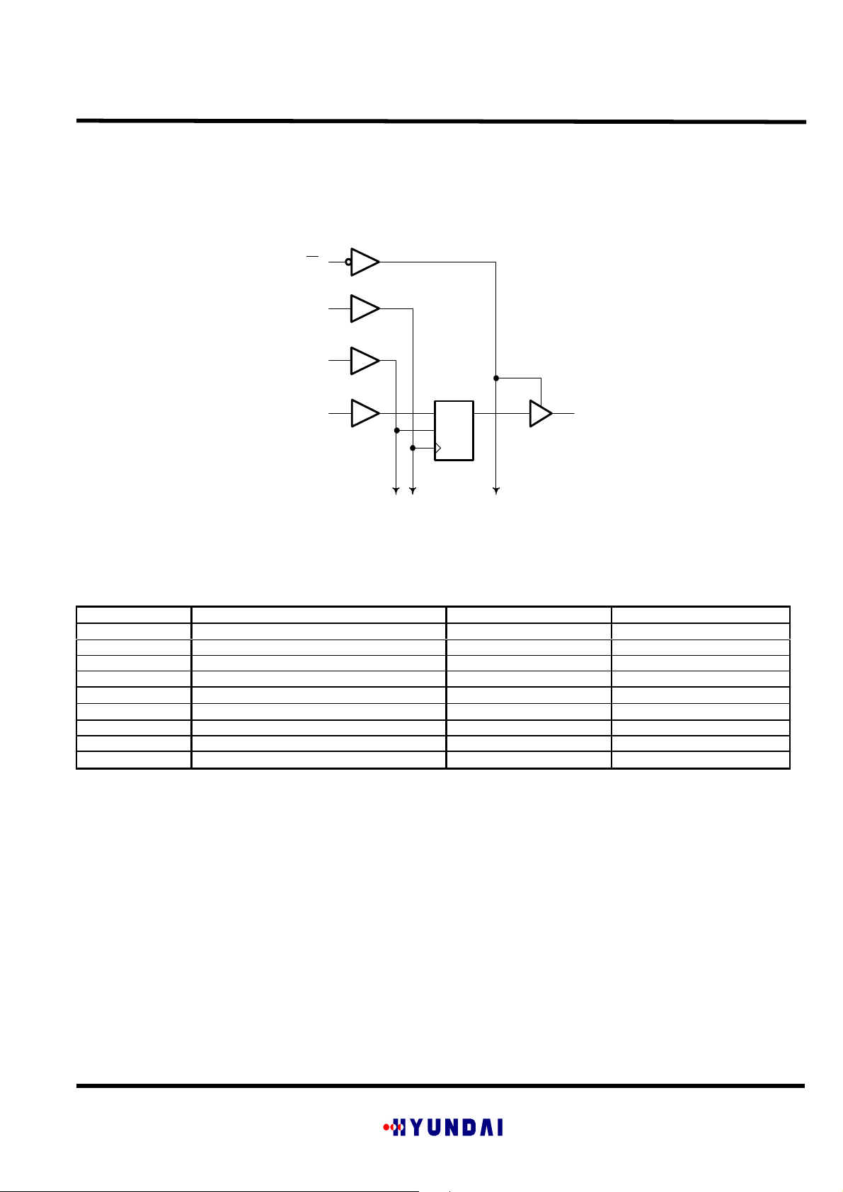
General Description
The HG74ALVC162835C is an 18-bit universal bus
driver designed for 2.3V to 3.6 V V
The Output Enable(OE) controls data flow from A to Y.
The device operates in transparent mode when the
latch-enable(LE) input is high. When LE is low, the A
data is latched if the clock input is held at a high or low
logic level. If LE is low, the A data is stored in the
latch/flip-flop on the low-to-high transition of CLK.
When OE is high, the Outputs are in the high
impedance state. OE should be tied to V
pull up resistor to ensure the high impedance state
during power up or power down.
The equivalent 26-Ω series resistors are included in
the output to reduce overshoot and undershoot.
The HG74ALVC162835C is characterized for operation
from -40°C to 85°C.
Function Table
INPUTS
LE CLK A
H X X X Z
L H X L L
L H X H H
L L
L L
↑
↑
L L L or H X Y
=Output level before the indicated steady-state input
conditions were established, provided that CLK is high
before LE goes low.
L L
H H
Operation.
CC
OUTPUT
Y
=
O
through a
CC
NC- No ineternal connection
Copyright©1999, Hyundai Electronics Industries Co., Ltd.
ELECTRONICS
18-BIT UNIVERSAL BUS DRIVER HG74ALVC162835C
WITH 3-STATE OUTPUTS Jan. 1999
Logic Diagram (positive logic)
27
OE
30
CLK
28
LE
54
A1 Y1
TO 17 Other Channels
1D
C1
CLK
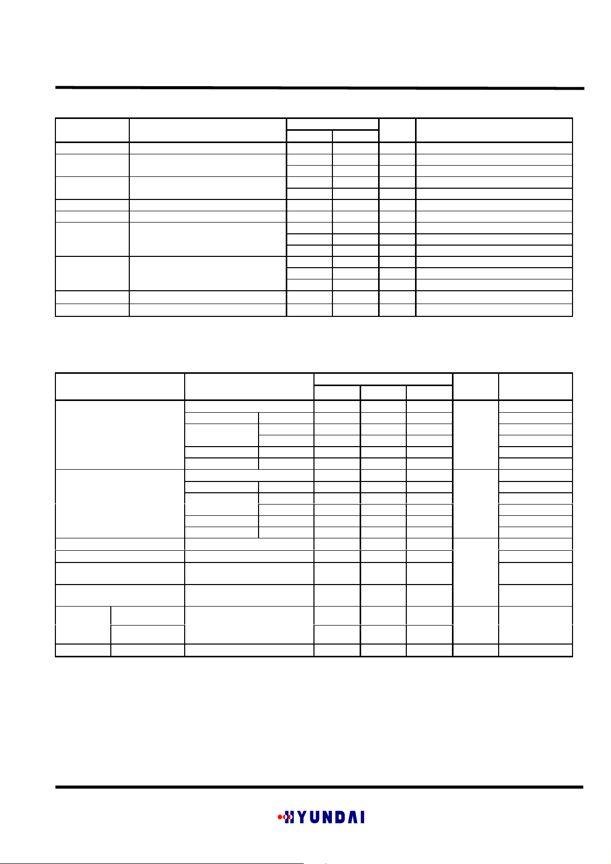
Absolute Maximum Ratings Over Operating Free-air Temperature Range
3
=
Symbols Parameter Value Conditions
V
CC
V
I
V
O
I
IK
I
OK
I
O
I
CC
I
GND
T
stg
=Stresses beyond those listed under “absolute maximum rating” may cause permanent damage to the device. These are stress ratings only, and
functional operation of the device at these or any other conditions beyond those indicated under “recommended operating condition” is not
implied. Exposure to absolute maximum-rated conditions for extended periods may affect device reliability.
Supply Voltage Range -0.5 V to 4.6 V
Input Voltage Range (see note 1) -0.5 V to VCC + 0.5 V
Output Voltage Range (see notes 1 and 2) -0.5 V to VCC + 0.5 V
Input Clamp Current -50 mA VI < 0
Output Clamp Current
Continuous Output Current
Continuous Current through each V
CC
±50 mA
±50 mA
+100 mA
VO <0 or VO >V
VO =0 to V
Continuous Current through each GND -100 mA
Storage Temperature Range
- 65°C to 150°C
CC
CC
Note 1) The input and output voltage ratings may be exceeded if the input and output clamp current are observed.
Note 2) This value is limited to 4.6 V maximum.
Copyright©1999, Hyundai Electronics Industries Co., Ltd.
ELECTRONICS
18-BIT UNIVERSAL BUS DRIVER HG74ALVC162835C
CC
WITH 3-STATE OUTPUTS Jan. 1999
Recommended Operating Conditions (see Note 3)
Symbols Parameter
V
CC
V
IH
V
IL
V
I
V
O
OH
I
OL
∆t/∆v
T
A
Note 3) All unused inputs of the device must be held at Vcc or GND to ensure proper device operation.
Supply Voltage 2.3 3.6 V
High -level input Voltage
Low-level input Voltage
Input Voltage 0 V
Output Voltage 0 V
High-level output current
Low-level output current
Input transition rise or fall rate 0 10 ns/V
Operating free-air temperature -40 85
Value
MIN MAX
Units Conditions
1.7 V VCC =2.3V to 2.7V
2 V VCC =2.7V to 3.6V
0.7 V VCC =2.3V to 2.7V
0.8 V VCC =2.7V to 3.6V
CC
CC
V
V
-6 mA VCC =2.3V
-8 mA VCC =2.7VI
-12 mA VCC =3V
6 mA VCC =2.3V
8 mA VCC =2.7V
12 mA VCC =3V
°C
Electrical Characteristics Over Recommended Operating Free-air Temperature Range
Value
Parameter Test Conditions
IOH = -100µA
IOH = - 4mA VIH =1.7V 1.9 2.3V
V
OH
IOH = - 8mA VIH = 2V 2 2.7V
IOH = -12 mA VIH = 2V 2
IOL = 100µA
IOL = 4mA VIL = 0.7V 0.4 2.3V
V
OL
IOL =8mA VIL = 0.8V 0.6 2.7V
IOL =12mA VIL = 0.8V 0.8
I
∆I
I
L
I
OZ
CC
CC
VI= VCC or GND
VO = VCC or GND
VI = VCC or GND
IO = 0
One input at VCC - 0.6V,
Other inputs at VCC or GND
Control Inputs
C
I
C
o
=
All typical Values are at VCC =3.3V, TA = 25°C.
Data Inputs
Outputs VO= VCC or GND
VI = VCC or GND
VIH =1.7V 1.7 2.3VIOH = - 6mA
VIH = 2V 2.4 3V
VIL = 0.7V 0.55 2.3VIOL = 6mA
VIL = 0.8V 0.55 3V
Min Typ= Max
V
- 0.2 2.3V to 3.6V
0.2 2.3V to 3.6V
±5
±10
40 3.6V
750
3.5
5
7
Units V
V
3V
V
3V
3.6V
3.6V
µA
3V to 3.6V
ρF
ρF
3.3V
3.3V
CC
Copyright©1999, Hyundai Electronics Industries Co., Ltd.
ELECTRONICS
 Loading...