

HEI HDM8513AT, HDM8513AP Datasheet

1
HDM8513A Users Manual
DVB/DSS Compliant Receiver
Nov. 2000
Revision 1.0
Electronics Industries Co., Ltd.

2
Direct Broadcast Satellite (DBS) has been one of the most successful new product
introductions in the history of consumer electronics. This product represents the first
application of digital video compression for broadcast television. Originally intended to
provide cable quality television services to remote areas, this product is now offering a
competitive replacement to cable services in many urban areas.
The first operational systems employ closed proprietary signaling structures. The
European Br oadcasting Union (EBU) has developed the first open standard (DVB-S) for
DBS services. The broadcasting community has embraced this standard which is now
being adopted for new systems throughout the world. This widely accepted open
standard is essential for DBS to achieve full market potential.
The HDM8513ATM is a fully DVB-S&DSS compliant ADC/QPSK demodulator/FEC
device which provides an MPEG-2 stream to be processed by the conditional access
and video decompression circuits. The demodulator clocked w ith a fixed frequency is
true variable rate over the range of 1 to 55M symbols-per-second. This product
achieves the highest performance and flexibility. It minimizes the cost of external
circuits, thus reducing overall system cost.

3
Hyundai Electronics Ind. Co., Ltd reserves the right to make changes to its products or
specifications to improve performance, reliability, or manufacturability. Information
furnished by Hyundai Electronics Ind. Co., Ltd is believed to be accurate and reliable.
However, no responsibility is assumed by Hyundai Electronics Ind. Co., Ltd for its use;
nor for any infringement of patents or other rights of third parties which may result from
its use. No license is granted by its implication or otherwise under any patent rights of
Hyundai Electronics Ind. Co., Ltd.
For more information contact:
Address: Youngdong Bldg. 891, Daechi-dong, Kangnam-gu, Seoul, 135 -738, Korea
Tel: 82-2 -3459-3188
Fax: 82-2 -3459-5843
E-mail: kosb@hei.co.kr

4
TABLE OF CONTENTS
1. INTRODUCTION TO THE HDM8513A ................................................................................................................6
1.1 FEATURES AND BENEFITS..................................................................................................................................7
2. HARDWARE SPECIFICATION..............................................................................................................................8
3. TECHNICAL OVERVIE W.....................................................................................................................................18
3.1 DUAL CHANNEL ANALOG TO DIGITAL CONVERTER .................................................................................. 18
3.2 V ARIABLE RATE DEMODULATOR.................................................................................................................. 20
3.3 NOISE MEASUREMENT CIRCUIT.....................................................................................................................22
3.4 V ITERBI DECODER.............................................................................................................................................24
3.5 AUTONOMOUS ACQUISITION..........................................................................................................................25
3.6 REED SOLOMON DECODER..............................................................................................................................27
3.7 CLOCK G ENERATION PLL .................................................................................................................................29
3.8 DBS R ECEIVER...................................................................................................................................................30
4. MECHANICAL SPECIFICATION S..................................................................................................................... 31
4.1 100 P IN Q UAD FLAT PACK................................................................................................................................31
4.2 64 P IN THIN QUAD FLAT PACK........................................................................................................................33
4.3 RECOMMENDED ANALOG P IN CONNECTION...............................................................................................35
4.4 RECOMMENDED CLOCK G ENERATION CIRCUIT...........................................................................................35
5. SIGNAL DESCRIPTION....................................................................................................................................... 36
5.1 INPUTS..................................................................................................................................................................36
5.2 OUTPUTS.............................................................................................................................................................36
5.3 MONITOR AND CONTROL INTERFACE ...........................................................................................................39
5.4 I2C MODE.............................................................................................................................................................40
6. REGISTER DEFINITIONS.....................................................................................................................................42
6.1 WRITE REGISTERS..............................................................................................................................................42
6.2 READ REGISTERS................................................................................................................................................55
APPENDIX....................................................................................................................................................................58
A1. L OOP FILTER PROGRAMMING APPLICATION NOTE................................................................................59
A2. FALSE LOCK ESCAPE APPLICATION NOTE.................................................................................................62
A3. PERFORMANCE WITH INTERFERENCE. .........................................................................................................63
A4. NYQUIST CRITERIA CONSIDERATIONS.........................................................................................................67
LIST OF FIGURES
FIGURE 1: T OP LEVEL BLOCK DIAGRAM....................................................................................................................6
FIGURE 2: I NPUT DATA TIMING DIAGRAM...............................................................................................................9
FIGURE 3: I NTEL 80C88A READ TIMING DIAGRAM...............................................................................................10
FIGURE 4: I NTEL 80C88A WRITE TIMING DIAGRAM.............................................................................................11
FIGURE 5: I NTEL 8051 READ TIMING DIAGRAM.....................................................................................................12
FIGURE 6: I NTEL 8051 WRITE TIMING DIAGRAM...................................................................................................13

5
FIGURE 7: MOTOROLA READ TIMING D IAGRAM....................................................................................................14
FIGURE 8: MOTOROLA WRITE TIMING DIAGRAM.................................................................................................15
FIGURE 9: O UTPUT TIMING DIAGRAM FOR NORMAL PARALLEL....................................................................... 16
FIGURE 10 : OUTPUT TIMING DIAGRAM FOR NORMAL SERIAL...........................................................................16
FIGURE 11: OUTPUT TIMING DIAGRAM FOR REGULATED PARALLEL...............................................................17
FIGURE 12: OUTPUT TIMING DIAGRAM FOR REGULATED SERIAL MODE1.......................................................17
FIGURE 13: OUTPUT TIMING DIAGRAM FOR REGULATED SERIAL MODE2.......................................................17
FIGURE 14: ADC B LOCK DIAGRAM............................................................................................................................ 19
FIGURE 15: DEMODULATOR BLOCK DIAGRAM .......................................................................................................20
FIGURE 16: NOISE MEASUREMENT CIRCUIT...........................................................................................................22
FIGURE 17: NOISE ACCUMULATOR AS A FUNCTION OF SNR AND TIME............................................................ 23
FIGURE 18: V ITERBI D ECODER...................................................................................................................................24
FIGURE 19: REED SOLOMON DECODER....................................................................................................................28
FIGURE 20: CLOCK SIGNAL G ENERATION................................................................................................................29
FIGURE 21: TYPICAL SET TOP BOX DEMODULATOR............................................................................................ 30
FIGURE 22: MECHANICAL CONFIGURATION...........................................................................................................32
FIGURE 23: MECHANICAL CONFIGURATION...........................................................................................................34
FIGURE 24: ANALOG PIN CONNECTION.................................................................................................................... 35
FIGURE 25: CLOCK GENERATION CIRCUIT ..........................................................................................................35
FIGURE 26: I2C WRITE TO THE HDM8513A ...........................................................................................................40
FIGURE 27 : I2C READ FROM THE HDM8513A .........................................................................................................41
FIGURE A1: SYMBOL TIMING RECOVERY TRANSIENT RESPONSE....................................................................... 59
FIGURE A2: CARRIER PHASE RECOVERY TRANSIENT RESPONSE........................................................................60
FIGURE A3: CARRIER PHASE RECOVERY TRANSIENT RESPONSE WITH LOW SNR..........................................61
FIGURE A4: ADJACENT CHANNEL INTERFERENCE OF 10 DB, 1.35 SPACING....................................................64
FIGURE A5: PERFORMANCE WITH INTERFERER AT DIFFERENT CARRIER SPACINGS.....................................65
FIGURE A6: PERFORMANCE WITH +10 DB INTERFERER......................................................................................66
LIST OF TABLES
TABLE 1: ABSOLUTE MAXIMUM RATINGS...............................................................................................................8
TABLE 2: DC C HARACTERISTICS.................................................................................................................................8
TABLE 3: D EMODULATOR SPECIFICATIONS.............................................................................................................9
TABLE 4: AC C HARACTERISTICS.................................................................................................................................9
TABLE 5: I NTEL 80C88A READ CYCLE TIMING PARAMETERS (B USMODE = 1)................................................10
TABLE 6: I NTEL 80C88A WRITE CYCLE TIMING PARAMETERS (BUSMODE = 1).............................................11
TABLE 7: I NTEL 8051 READ CYCLE TIMING PARAMETERS (BUSMODE = 1)......................................................12
TABLE 8: I NTEL 8051 WRITE CYCLE TIMING PARAMETERS (BUSMODE = 1)...................................................13
TABLE 9: MOTOROLA READ CYCLE TIMING PARAMETERS (BUSMODE =0).................................................... 14
TABLE 10: MOTOROLA WRITE CYCLE TIMING PARAMETERS (BUSMODE =0).................................................15
TABLE 11: OUTPUT TIMING....................................................................................................................................... 16
TABLE 12: E XAMPLE OF ACQUISITION TIMING.....................................................................................................26
TABLE 13: I2C S LAVE ADDRESS..................................................................................................................................41
6
6
6
I
Q
DemodulatorViterb
i
and
Solomon
8Data ClockDataQPSKNode
Fixed Rat
e
Sample Clock33Symbol ClockViterbi Bit ClockFrameSync8Viterb
i
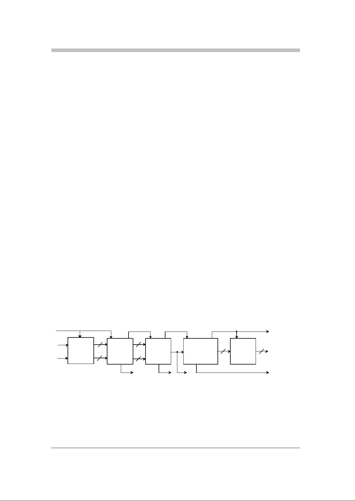
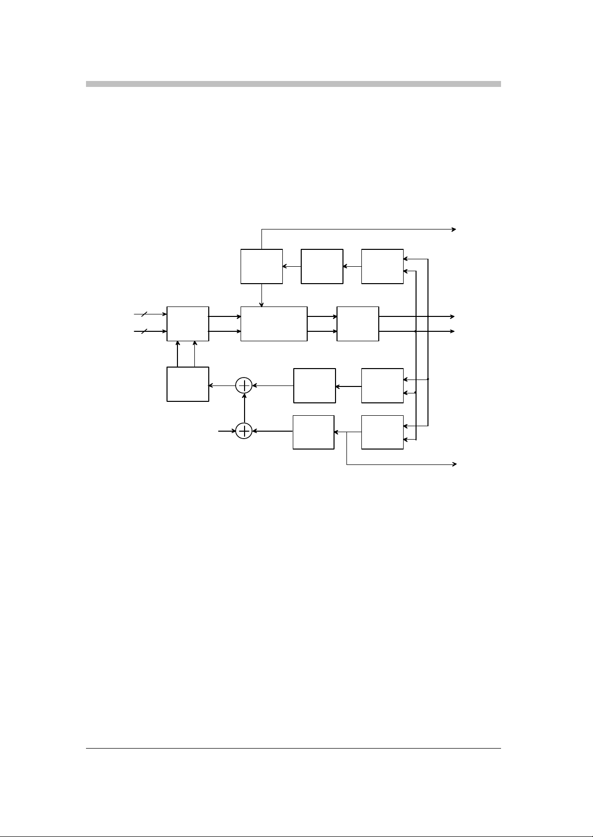
1. Introduction to the HDM8513A
The HDM8513A digital demodulator for direct broadcast satellite receivers is a single chip solution fully
compliant with the European Telecommunications Standards Institute (ETSI) specification ETS 300
421. This chip integrates an A/D converter, a variable rate matched filter, a variable rate QPSK
demodulator with a Viterbi decoder, a deinterleaver and a Reed Solomon decoder.
The HDM8513A, which is implemented in a 0.35 micron CMOS, Triple Layer Metal Process, provides
variable rate capability while operating with a fixed frequency sampling clock. Digital samples of
baseband I and Q data are generated by an internal A/D converter, then provided to the demodulator at
a fixed sample rate. The root raised cosine filter is implemented internally with fully digital techniques.
Similarly, the symbol timing recovery and carrier phase tracking functions are performed entirely in the
digital domain. This approach provides minimum constraints on external circuits, thus reducing overall
system costs.
The HDM8513A may be configured by an external processor for a specific symbol rate, and carrier
frequency along with loop gain parameters. The HDM8513A provides an external AGC signal which is
used to control the gain of the analog signal which is applied to the down-converters. And it also
provides a digital AGC internally which controls the gain of the signal out of the matched filters. In
addition, the HDM8513A provides fully programmable sweep circuitry to aid in initial acquisition when
large frequency offsets may be present.
The digital frequency translation capability of the HDM8513A permits this part to be used in frequency
multiplexing applications. In this application, an entire transponder bandwidth containing many signals
is sampled at a fixed rate. The digital oscillator within the HDM8513A is programmed to the specific
desired carrier frequency within that band to permit the selected signal to be passed through the
baseband filter and processed by the demodulator circuits.
A/D
Converter
Variable
Rate
QPSK
Decoder
Synchronization
Deinterleaving
Reed
Decoder
FIGURE 1: T OP LEVEL BLOCK DIAGRAM

7
1.1 Features and Benefits
* Fully DVB&DSS compliant
* Dual 6bit A/D converters
* Continuously variable symbol rate from 1Msps to 55Msps (75MHz clock)
* Internal digital root raised cosine filter
* Less than 0.5 dB implementation loss
* Frequency multiplexing capability
* Automated frequency search
* Internal bias cancellation
* Both wideband and narrowband AGC
* Noise calibration for antenna steering
* Output data rate as high as 68Mbps
* Fixed frequency sampling clock
* Simple interface with tuner and analog processing
* Microcontroller interface
* Eight bit parallel or I2C monitor and control interface
* I2C by -pass mode
* Two package types
Part code Package
HDM8513AP 100PQFP
HDM8513AT 64TQFP
8
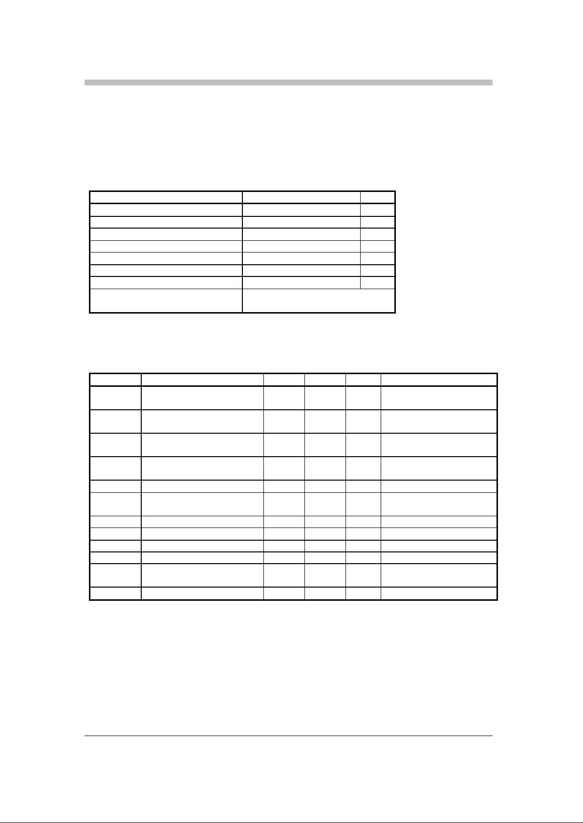
2. Hardware Specification
Table 1: Absolute Maximum Ratings
Rating Value Unit
Ambient Temperature under Bias -10 to 70 c
Storage Temperature -65 to 150 c
Ambient Humidity under Bias 85( 85 c,500hrs) %
Thermal Resistance(Ja) 45 c/W
Junction Temperature 150 c
Voltage on Any Pin Vss - 0.3V to VDD + 0.5V V
VDD, IOVDD 5.5 V
Package Material - Compound : CEL -4630SX
Table 2: DC Characteristics
Symbol Parameter Min. Max. Units Test Conditions
IDD Dynamic Current
(Power Supply Current)
IOVDD Interface Power Supply
Voltage
VDD Core Power Supply
Voltage
V ADC Power Supply
Voltage
VIL Input Low Voltage 0 0.3VDD V
VIH Input High Voltage 0.7VDD VDD+
VOL Output Low Voltage - 0.4 V I
VOH Output High Voltage 2.4 - V IOH = 4 mA
IIH Input High Current -10 10 uA VIL = VDD
IIL Input Low Current - 10 10 uA VDD = 3.6, VIL =0.5
CIN Input Capacitance
(analog pad)
COUT Output Capacitance - 10 pF Typical 8.83pF
(IOVDD and VDD = 3.3V + or - 5%, TA = 0 to 70 c, unless otherwise specified)
- Lead Frame : Copper
- 395 mA VDD=3.3, Freq=60Mhz
3 3.6 V Normal Operation
3 3.6 V Normal Operation
3 3.6 V Normal Operation
0.5
- 10
10
(Typical 367mA)
V
OL
= 4 mA
pF Typical 8.76pF
(8.52pF)
9
CLOCK
I_IN [5:0]
or Q_IN [5:0]
Table 3: Demodulator Specifications
Parameter Min. Max.
Sampling Clock Frequency 1MHz 75MHz
Analog Input Full Scale Range 0.9 Vpp 1.1 Vpp
Symbol Rate 1Msps 55Msps
Viterbi Data Rate - 75Mbps
Reed Solomon Data Rate - 69Mbps
Implementation Loss - 0.5 dB
Symbol Rate Resolution Clock/(220) Carrier Frequency Resolution Clock/(220) Acquisition Sweep Range - + or - Clock/2
Table 4: AC Characteristics
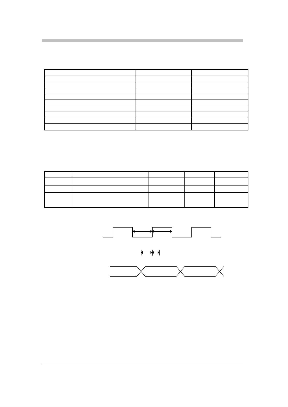
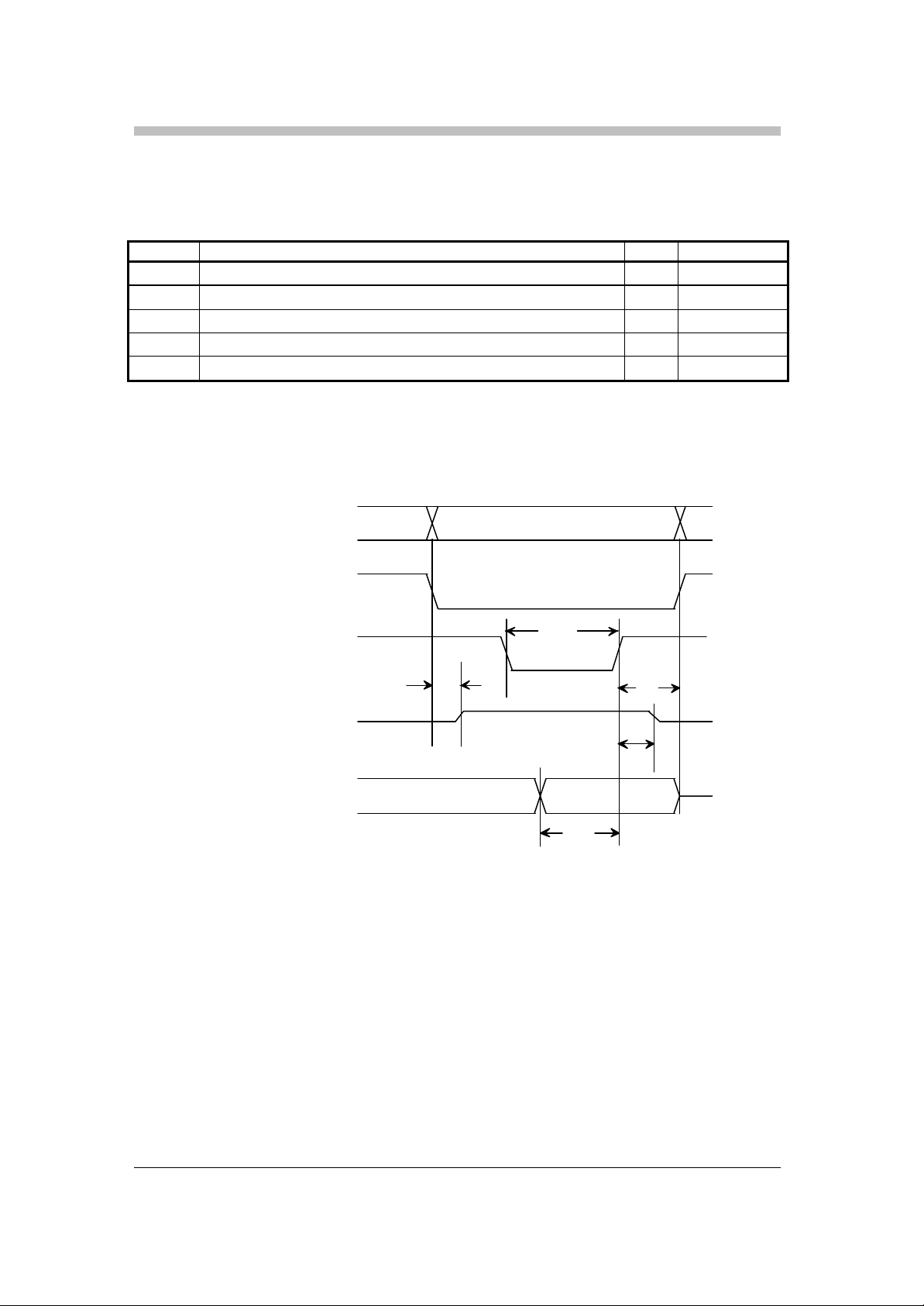
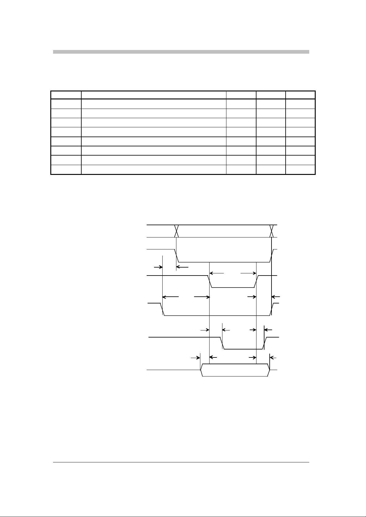
Symbol Parameter Min. Max. Unit
t
Input Data Setup before Clock 6 - ns
su1
th1 Input Data Hold after Clock 2 - ns
t
Low Pulse Width of Clock 8.7 - ns
pw1
t
High Pulse Width of Clock 8.1 - ns
pw2
tpw1
t
pw2
t t
su1 h1
F IGURE 2: INPUT DATA TIMING DIAGRAM
10
Valid
HI_ADDR [4:0]
/CE
/REDTACKHI_D
A
TA[7:0]
t
t
t
t
t
t
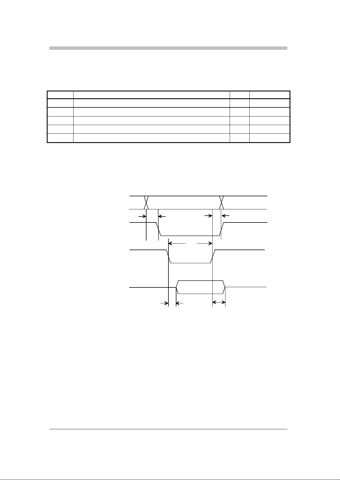
Table 5: Intel 80C88A Read Cycle Timing Parameters (Busmode = 1)
Symbol Parameter Min. Max. Unit
t
Input Address and /CE Setup before /RE Inactive 35 - ns
su1
th1 Input Address and /CE Hold after /RE Inactive 5 - ns
t
/RE Low Duration 200 - ns
pw1
td1 Delay from /CE to DTACK Active - 35 ns
t
Delay from /RE Inactive to DTACK in Tristate Mode - 10 ns
doz1
t
Delay from /RE Inactive to HI_DATA [7:0] Tristate Mode 10 - ns
doz2
pw1
d1
Z
su1
FIGURE 3: I NTEL 80C88A READ TIMING DIAGRAM
Note: HI_ADDR[4:0] is derived from the processor(80C88A) A15-A8 bus and HI_DATA[7:0] is
connected to the AD7 - AD0 bus.
#This page is only for HDM8513AP.
h1
Z
doz1
doz2
11
Valid
HI_ADDR [4:0]
/CE
/WE
DTACKHI_DATA[7:0]
th1t
t
t
t
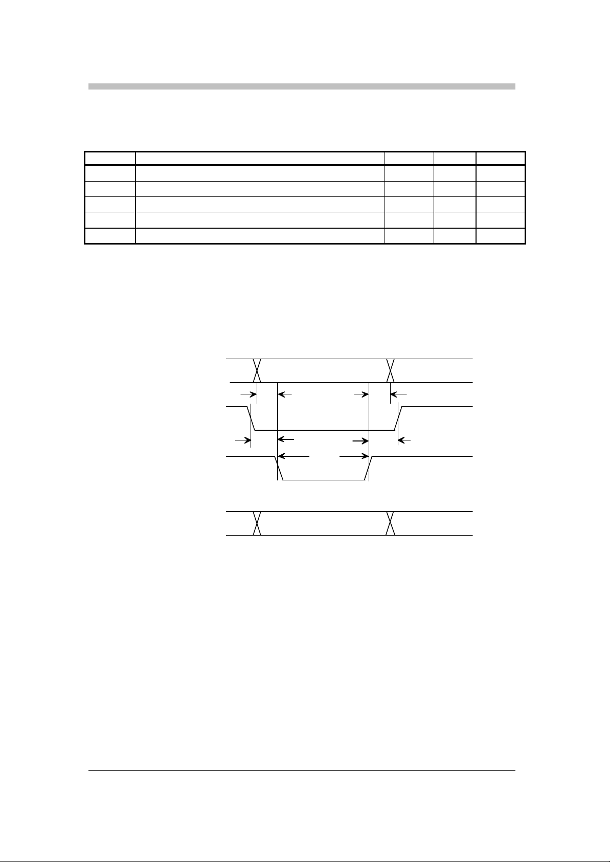
Table 6: Intel 80C88A Write Cycle Timing Parameters (Busmode = 1)
Symbol Parameter Min. Max. Unit
t
Input Data Setup before /WE Inactive 20 - ns
su1
th1 Input Address, Data and /CE Hold after /WE Inactive 8 - ns
t
/WE Low Duration 200 - ns
pw1
td1 Delay from /CE to DTACK Active - 35 ns
t
Delay from /WE Inactive to DTACK in Tristate Mode - 15 ns
doz1
pw1
d1
doz1
su1
FIGURE 4: INTEL 80C88A WRITE TIMING DIAGRAM
Note: HI_ADDR[4:0] is derived from the processor(80C88A) A15-A8 bus and HI_DATA[7:0] is
connected to the AD7 - AD0 bus.
#This page is only for HDM8513AP.
12
Valid
HI_ADDR [4:0]
/CE
/REHI_DATA[7:0]
t
t
t
t
t
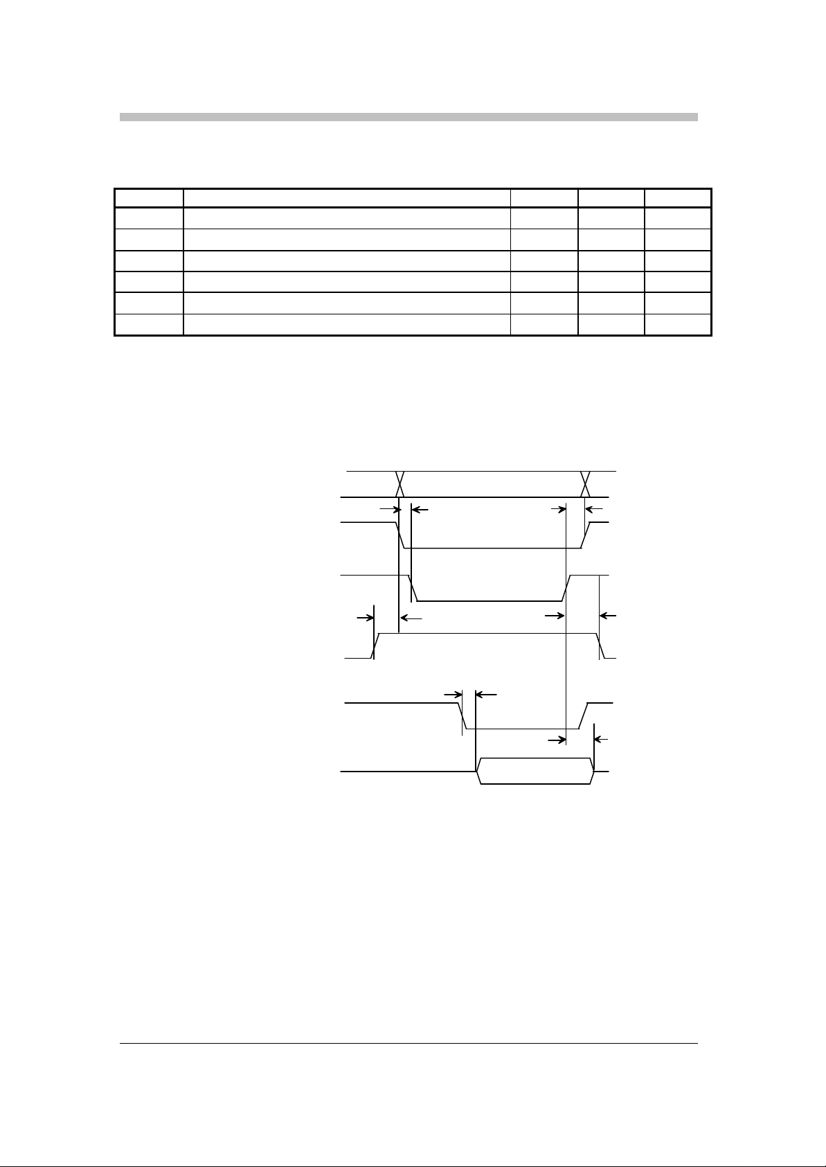
Table 7: Intel 8051 Read Cycle Timing Parameters (Busmode = 1)
Symbol Parameter Min. Max. Unit
t
Input Address Setup before /CE Active 5 - ns
su1
th1 Input Address and /CE Hold after /RE Inactive 5 - ns
t
/RE Active Duration 400 - ns
pw1
t
Delay from /RE Active to HI_DATA [7:0] Valid - 40 ns
pd1
t
Delay from /RE Inactive to HI_DATA[7:0] Tristate Mode 10 - ns
doz1
FIGURE 5: I NTEL 8051 READ TIMING DIAGRAM
#This page is only for HDM8513AP.
su1
pd1
h1
pw1
doz1
13
Valid
HI_ADDR [4:0]
/CE
/WE
HI_DATA[7:0
]
t
t
t
Valid
t
t
Table 8: Intel 8051 Write Cycle Timing Parameters (Busmode = 1)
Symbol Parameter Min. Max. Unit
t
Input Address and Data Setup before /WE Active 5 - ns
su1
th1 Input Address and Data Hold after /WE Inactive 5 - ns
t
/WE Active Duration 400 - ns
pw1
t
/CE Setup to /WE Active 5 - ns
su2
th2 /CE Hold after /WE Inactive 5 - ns
FIGURE 6: I NTEL 8051 WRITE TIMING DIAGRAM
#This page is only for HDM8513AP.
su2
su1
h1
h2
pw1
14
Table 9: Motorola Read Cycle Timing Parameters (Busmode =0)
Symbol Parameter Min. Max. Unit
t
Setup Time of R/W with respect to /CE Active 5 - ns
su1
t
Address Setup with respect to /DS Active 5 - ns
su2
td1 Delay from DTACK Active to Data Valid - 30 ns
th1 R/W Hold with respect to /DS Inactive 5 - ns
th2 Address Hold with respect to /DS Inactive 5 - ns
th3 Data Hold with respect to /DS Inactive 10 - ns
HI_ADDR[4:0]
t
su2
/CE
/DS
t
su1
R/W
DTACK
HI_DATA[7:0]
FIGURE 7: MOTOROLA READ TIMING D IAGRAM
Note: External pull-up resistor is required on DTACK.
#This page is only for HDM8513AP.
Valid
t
d1
t
h2
t
h1
t
h3
15
/CS
/DS
HI_DATA[7:0]
t
ttt
t
Table 10: Motorola Write Cycle Timing Parameters (Busmode =0)
Symbol Parameter Min. Max. Unit
t
Data Setup to /DS Active 5 - ns
su1
t
R/W Setup to /CS and Address 3 - ns
su2
td1 /DS Delay from R/W 5 - ns
td2 DTACK Delay from /DS Active - 40 ns
td3 DTACK Delay from /DS Inactive - 10 ns
t
/DS Active Duration 5 - ns
pw1
th1 Address, /CS and R/W Hold from /DS Inactive 5 - ns
th2 Data Hold from /DS Inactive 5 - ns
HI_ADDR[4:0]
su2
d1
R/W
DTACK
t
su1
FIGURE 8: MOTOROLA WRITE TIMING D IAGRAM
Note: External pull up resistor is required on DTACK.
#This page is only for HDM8513AP.
Valid
d2
t
pw1
Valid
h1
d3
t
h2
16
1234n
n-1
n-2
n-3xxxxxxxxxxxxxxxx
xx
12348n-5
8n-6
8n-7
8n-8xxxx
xxxx8n-4
8n-3
8n-2
8n-1
8n
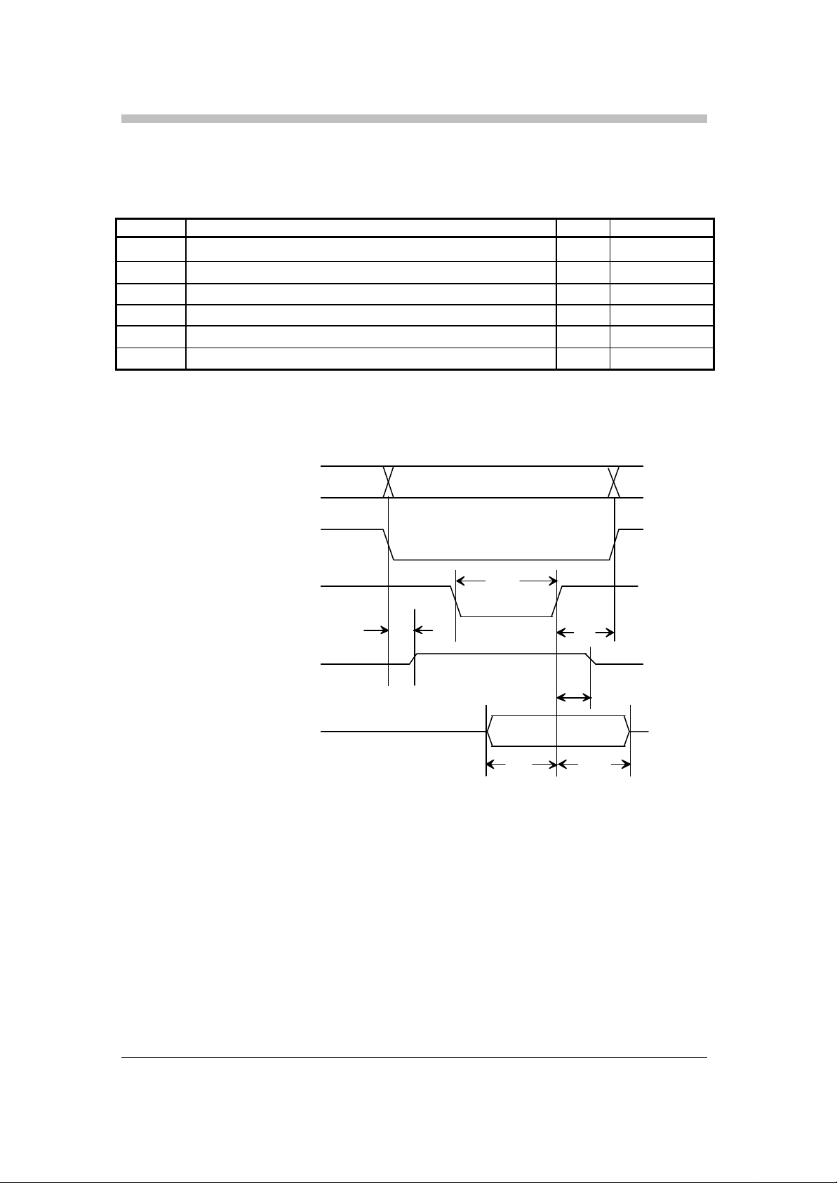
Table 11: Output Timing
Symbol Parameter Min. Max. Unit
tsu Output Data Setup before DATA_CLK and DATA_STB 5 - ns
thd Output Data Hold after DATA_CLK and DATA_STB 10 - ns
t
t
su
hd
DATA_CLK
DATA_STB
FRAME_SYNC
DATA_VALID
DATA
FIGURE 9: O UTPUT TIMING DIAGRAM FOR NORMAL PARALLEL
DATA_CLK
DATA_STB
FRAME_SYNC
DATA_VALID
DATA[0]
FIGURE 10: O UTPUT TIMING DIAGRAM FOR NORMAL SERIAL
NOTE : In case of DVB, n is 188
In case of DSS, n is 144
t
t
su
hd
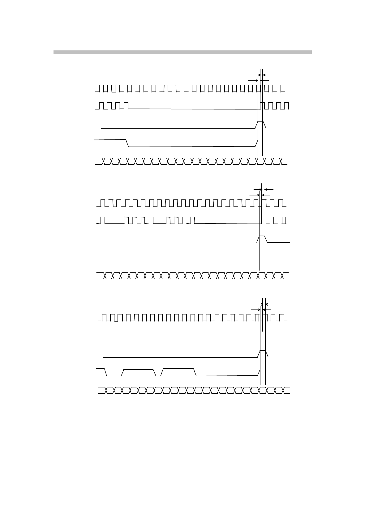
17
123
4
n-1
n-2
n-3
xxxxxxxxxxxxxxxxxxxxxxxxxxxxxx
xx
n
12348n-5
8n-6
8n-7
8n-4xxxxxxxxxxxxxxxx
xx
8n-8xxxx
8n-3
8n-2
8n-1
8n
123
4
8n-7
8n-4
8n
8n-8xxxx
xx
xxxxxxxxxxxxxx
xx
8n-5
8n-6
8n-1
8n-2
8n-3
DATA_CLK
DATA_STB
FRAME_SYNC
DATA_VALID
DATA
DATA_CLK
DATA_STB
t
su
FIGURE 11 : OUTPUT TIMING DIAGRAM FOR REGULATED PARALLEL
t
su
t
hd
t
hd
FRAME_SYNC
DATA[0]
FIGURE 12: O UTPUT TIMING DIAGRAM FOR REGULATED SERIAL MODE1
DATA_CLK
FRAME_SYNC
DATA_STB
DATA[0]
FIGURE 13: O UTPUT TIMING DIAGRAM FOR REGULATED SERIAL MODE2
NOTE : In case of DVB, n is 188
In case of DSS, n is 144
t
t
su
hd

18
3. Technical Overview
3.1 Dual Channel Analog to Digital Converter
The block diagram shown below illustrates internal configuration of the Dual Channel ADC.
Baseband signals, in -phase(I) and quadrature phase(Q), which are generated by down converters,
are applied to the dual channel ADC and quantized to 6-bit digital codes respectively. The ADC is
optimized to allow AC coupled inputs with full scale input range of 1V + or - 10%. An LSB weight is
approximately 15.6 mV.
The full scale input analog conversion range (Vpp) is determined by the voltages of VTOP and
VBOT and simply equal to (VTOP - VBOT). The full scale range is defined as the voltage range that
accommodates 63 codes of equally spaced LSBs. Also the ADC supplies its own reference
voltages for A/D conversions. The voltages can be monitored by external reference pins. The
VTOP, VBOT represent top and bottom reference voltages respectively. REF_I, REF_Q represent
middle reference voltages for each channel. All these 4 reference voltage pins should be by -passed
to GND via 0.1uF capacitors. The values of internally generated voltage of VTOP and VBOT are
2.0V and 1.0V respectively. Vpp can be adjusted by externally applying voltages to both VTOP
and VBOT pins respectively when different conversion ranges are necessary. VTOP can be
adjusted as high as 2.3V and VBOT can be as low as 0.5V. A larger input range can be
established by taking VTOP higher and VBOT lower than on -chip generated voltages.
To supply necessary bias voltages for AC coupled applications, REF_I and REF_Q, which are
middle reference voltages for I and Q channel, are connected to the analog input pins (AIN_I and
AIN_Q ) respectively through 40 kohm resistors, as shown in the block diagram. For DC coupled
applications, these voltages can be used to feed back offset compensation signals.
To insure optimum performance, a low impedance analog ground plane is recommended and
should be separated from other digital ground planes. The analog power supplies should be bypassed at device to analog ground through 0.1uF ceramic capacitors.
19
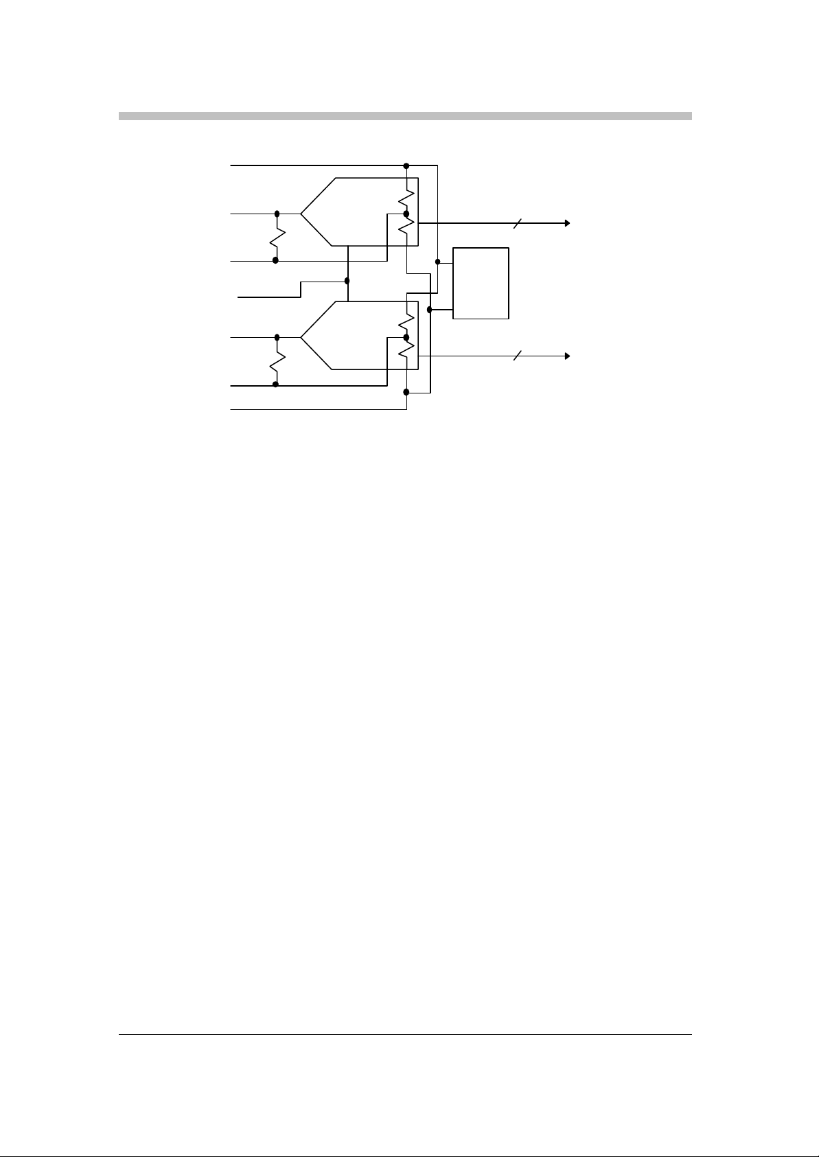
AIN_Q
VBOT
CLOCK
REF_I
REF_Q
VTOP
AIN_I
6-bit ADC
Ref.
Voltage
Gen.
6-bit ADC
FIGURE 14: ADC B LOCK DIAGRAM
6
6
DI
DQ
20
Multiplie
r
Filters
AGC
s
s
SymbolTimingDiscriminatorSymbolTrackingLoop FilterPhase
Accumulator
SineCosin
e
CarrierTrackingLoop FilterNominal Carrier FrequencyCarrierPhaseDiscriminator
Q
o
o
LockDetecto
r
LockSweepContro
l
3.2 Variable Rate Demodulator
The block diagram illustrates the overall configuration of the variable rate QPSK demodulator.
Baseband in-phase (I) and qu adrature (Q) inputs are applied to the demodulator at a fixed sampling
rate. These digital samples are produced by A/D converters which employ AC coupling to minimize
DC offset.
Symbol Clock
6
I
6
Q
Complex
Polyphase
Narrowband
I
Digital
Oscillator
FIGURE 15: DEMODULATOR BLOCK DIAGRAM
The carrier frequency error associated with these samples is removed digitally during tracking
operations by a complex multiplier and a digitally controlled oscillator, sometimes called a
numerically controlled oscillator (NCO). During initial acquisition, coarse frequency error is
removed by a combination of the digital AGC within the HDM8513A and external analog tuning
circuits.
A polyphase filter performs the root raised cosine filtering of the frequency corrected baseband
samples. This filter, which implements the function of equation (1), is always configured to have an
impulse response duration of 4 symbols regardless of the programmed symbol rate. For low
symbol rates, a large number of samples are used, while for high symbol rates a relatively low
number of samples are processed for each filter output. The outputs of the polyphase filters are
applied to a digital narrowband AGC which insures that the signal is optimally scaled to the Viterbi
decoder to an accuracy of + or - 0.5 dB to insure optimum FEC performance.
y[k] = Σ h[n] x[k- n] (1)
In addition to optimizing performance of the Viterbi decoder, the digital narrowband AGC also
insures that the performance of the symbol timing and carrier tracking loops is independent of

21
signal level variations. An analog wideband AGC is also employed to insure that the analog signal
applied to the A/D converters is properly scaled.
Both the symbol timing and carrier tracking loops are implemented digitally, which eliminates the
need for external connections to analog tuning components during steady state operation. This
causes the requirements on the analog presampling filter to be relaxed, permitting a lower cost
analog front end. For systems which require a narrowband presampling filter, and have the potential
for significant frequency error in the LNB (several MHz) the HDM8513A provides a high resolution
measure of carrier frequency to permit periodic readjustment of the front end tuner frequency to
compensate for drift. The host processor periodically reads the frequency register, then computes
appropriate correction to the tuner frequency.
The nominal symbol rate and the nominal carrier frequency are programmed into the demodulator
to an accuracy provided by 20 bits of resolution, and the system accuracy is equivalent to that of
the fixed frequency sampling clock.
During initial acquisition, the HDM8513A provides an automated sweep program to facilitate carrier
acquisition. The host processor loads a 20 bit register which determines the initia l carrier
frequency. A 16 bit register is programmed with the number of symbol times the receiver will dwell
at each frequency. If the receiver remains at the initial frequency for the programmed number of
symbol times without achieving lock, the carrier frequency is incremented by the step frequency
value programmed into another 16 bit register. If no lock is achieved, the receiver will continue to
increment the frequency until the maximum number of search frequencies, as determined by the
value in an eight bit register, is achieved. When the maximum number of search frequencies is
reached, the carrier frequency returns to the initial value and the entire process is repeated. Once
the host processor determines that lock is achieved by observing the loc k flag, it then inhibits the
sweep function and programs loop bandwidth parameters which are optimized for steady state
performance.
 Loading...