

Features
l Phase-Locked Loop Clock Distribution for
Synchronous DRAM Applications
l Supports PC-100 and Meets “PC100 SDRAM
registered DIMM Specification Rev. 1.2”
l Distributes One Clock Input to One Bank of Ten
Outputs
l No External RC Network Required
l External Feedback (FBIN) Pin is Used to
Synchronize the Outputs to the Clock Input
l Separate Output Enable for Each Output Bank
l Operates at 3.3 V Vcc
l 125 MHz Maximum Frequency
l On-chip Series Damping Resistors
l Support Spread Spectrum Clock(SSC)
Synthesizers
l ESD Protection Exceeds 3000 V per MIL-STD-
883, Method 3015 ; Exceeds 350 V Using
Machine Model ( C = 200 pF, R = 0 )
l Latch-Up Performance Exceeds 400 mA per
JESD 17
l Packaged in Plastic 24-Pin Thin Shrink Small-
Outline Package
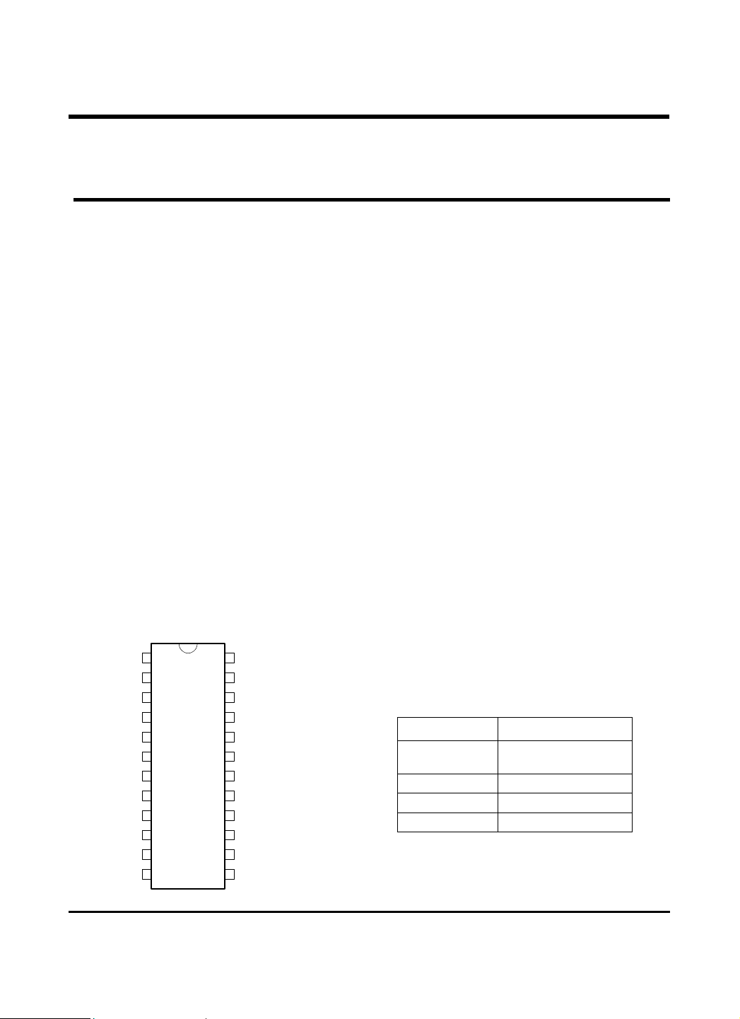
Pin Configuration
TSSOP 24 PACKAGE
(TOP VIEW)
AGND
Vcc
1Y0
1Y1
1Y2
GND
GND
1Y3
1Y4
Vcc
G
FBOUT
1
2
3
4
5
6
7
8
9
10
11
12
24
23
22
21
20
19
18
17
16
15
14
13
CLK
AVcc
Vcc
1Y9
1Y8
GND
GND
1Y7
1Y6
1Y5
Vcc
FBIN
HC2510C
HC2510C
General Description
The HC2510C is a low-skew, low jitter, phase-
locked loop(PLL) clock driver, distributing high
frequency clock signals for SDRAM.
The HC2510C operates at 3.3V Vcc and provides
integrated series-damping resistors that make it ideal
for driving point-to-point loads. The propagation delay
from the CLK input to any clock output is nearly zero.
Ten outputs provide low-skew and low-jitter clocks.
All outputs can be enabled or disabled via the control
input(G). Output signal duty cycles are adjusted to 50
percent, independent of the duty cycle at CLK.
The HC2510C is specially designed to interface with
high speed SDRAM applications in the range of
25MHz to 125MHz and includes an internal RC
network which provides excellent jitter characteristics
and eliminates the needs for external components.
For the test purpose, the PLL can be bypassed by
strapping AVcc to ground.
The HC2510C is characterized for operation from 0°C
to 85°C.
Function Table
INPUTS OUTPUTS
1Y
(0:9)
FBOUT
G CLK
X L L L
L H L H
H H H H
1
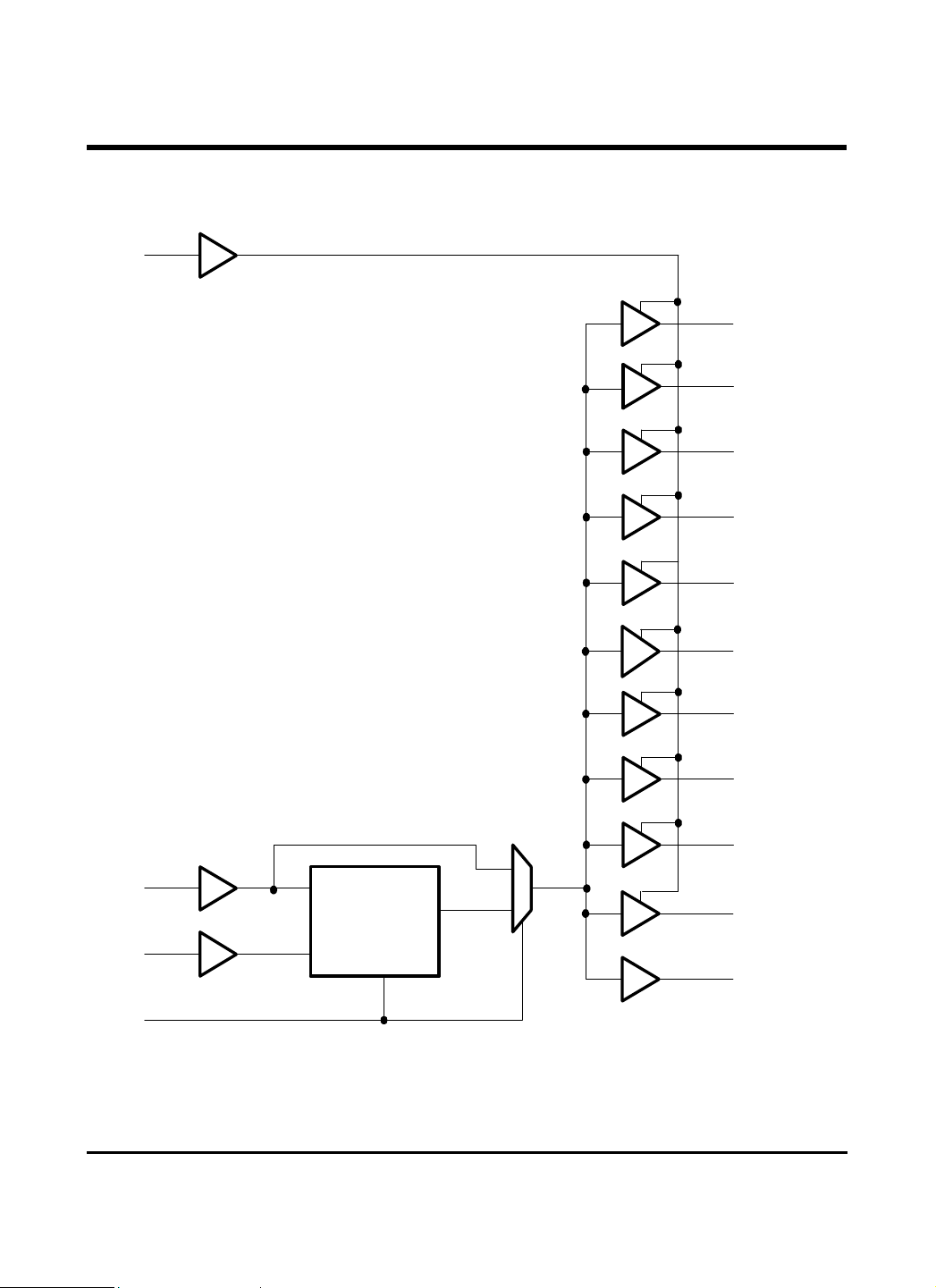
Functional Block Diagram
11
G
HC2510C
3
4
5
8
9
15
16
17
1Y0
1Y1
1Y2
1Y3
1Y4
1Y5
1Y6
1Y7
CLK
FBIN
AV
20
1Y8
24
21
PLL
1Y9
13
12
FBOUT
2 3
CC
2
 Loading...