


H1A424M167
Image Signal Processor
for Hyundai CMOS Image Sensor
Data Sheet
Version 1.0
Electronics Industries Co., Ltd
Hyundai Electronics Industries Co., Ltd. H1A424M167
REVISION HISTORY
Revision Issue Date Comments
0.45 April 28, 1999 Draft
0.9 June 15, 1999 Added Suspend Pin(No.16)
Added Flicker Free Banding noise filter
Added Histogram Equalization function
Added STATUS_FLAGS register
Modified Gamma Correction function
Modified AWB/AE function
0.95 August 10, 1999 Added CIF type CIS(HV7121X) support function
Added X-flip function
Modified Edge Enhancement filter
JFIF color space conversion equation
Modified BASE_ENB register
Modified STATUS_FLAGS register
Modified AWB/AE function
1.0 October 11, 1999 Added Functional Description/Register Description
Added Soldering Description
Formal Release
1999 October 11 Page 2

Hyundai Electronics Industries Co., Ltd. H1A424M167
TABLE OF CONTENTS
1. FEATURES......................................................................................................................................5
2. PIN CONFIGURATION..................................................................................................................6
3. PIN DEFINITION............................................................................................................................7
4. SYSTEM DIAGRAM.....................................................................................................................10
5. BLOCK DIAGRAM ......................................................................................................................10
6. VIDEO PROCESSING ENGINE BLOCK DIAGRAM............................................................... 11
7. FUNCTIONAL DESCRIPTION....................................................................................................12
7.1. HOST INTERFACE .......................................................................................................................12
7.1.1. Serial Interface..................................................................................................................12
7.1.2. Host Parallel Interface ...................................................................................................... 14
7.1.3. Serial or Parallel Interface selection .................................................................................15
7.2. CLOCK(MCLK, PCLK, VCLK) TIMING DIAGRAM .....................................................................16
7.3. VIDEO OUTPUT INTERFACE......................................................................................................... 16
7.4. RELATIONS BETWEEN INPUT VIDEO TIMING AND OUTPUT VIDEO TIMING ........................................ 17
7.4.1. VGA................................................................................................................................... 18
7.4.2. CIF....................................................................................................................................18
7.4.3. SIF..................................................................................................................................... 19
7.4.4. QCIF ................................................................................................................................. 19
7.4.5. QSIF..................................................................................................................................20
8. REGISTER DESCRIPTION .........................................................................................................21
8.1. REGISTERS MNEMONIC TABLE....................................................................................................21
8.2. BASE REGISTER MAP................................................................................................................ 24
8.2.1. Normal Register[80h~83h]................................................................................................ 24
8.2.2. Color Matrix Coefficients Value[8Ah ~ 95h]..................................................................... 26
8.3. AUTO REGISTER MAP...............................................................................................................29
8.3.1. Function Enable Register[A0h]......................................................................................... 29
8.3.2. AWB/AE Windows Configuration Registers[A1h~A6h]......................................................30
8.3.3. Normal Register[A7h~B8h]............................................................................................... 31
8.4. OUT REGISTER MAP..................................................................................................................37
8.4.1. Normal Register[C0h~C2h]............................................................................................... 37
1999 October 11 Page 3

Hyundai Electronics Industries Co., Ltd. H1A424M167
8.4.2. Histogram Equalization Control Register[C3h~C4h] ........................................................ 38
8.4.3. Gamma Control Register[E0h~F1h] .................................................................................. 39
9. ELECTRICAL CHARACTERISTICS .........................................................................................42
9.1. ABSOLUTE MAXIMUM RATINGS .................................................................................................. 42
9.2. DC CHARACTERISTICS...............................................................................................................42
9.3. AC CHARACTERISTICS...............................................................................................................43
9.3.1. Microcontroller Bus Interface timing (Write cycle)............................................................43
9.3.2. Microcontroller Bus Interface timing (Read cycle)............................................................. 43
9.3.3. Serial Interface Control Timing ......................................................................................... 44
9.3.4. RESETB Timing ................................................................................................................. 45
9.3.5. Video Output Timing.......................................................................................................... 45
10. PACKAGE SPEC......................................................................................................................... 46
11. SOLDERING................................................................................................................................47
11.1. SOLDER REFLOW EQUIPMENT .................................................................................................... 47
11.2. REFLOW PROFILES.................................................................................................................... 47
11.3. FLUX APPLICATION................................................................................................................... 47
11.4. CLEANING ............................................................................................................................... 47
11.5. DRYING................................................................................................................................... 47
1999 October 11 Page 4

Hyundai Electronics Industries Co., Ltd. H1A424M167
1. Features
n Dedicated sensor control and signal processing chip for Hyundai CMOS Image
Sensor
n CMOS 3.3V Device (0.5um CMOS TLM Process used)
n Serial-Bus interface or alternative 8-bit MCU parallel interface
for register programming
n Serial-Bus interface for HYUNDAI CMOS Image Sensor Chip Control
n 8 bit Bayer format image input
n 3 x 3 Interpolation
n Color Correction matrix
n Gamma Correction
n Automatic Exposure Control
n Automatic White Balance Control
n Programmable AE/AWB windows
n Automatic Reset Level Control
n Edge Enhancement Support
n 2x2, 4x4 Sub-Sampling(CIF, QCIF)
n RGB to YCrCb Color Space Convert
n Histogram Equalization Logic
n 16bit YUV 4:2:2, YUV 4:2:0, 8bit YUV 4:2:2, YUV 4:2:0 video output format
n Flicker Free Banding noise filter
n X Flip Function for mirrored image
n Horizontal and Vertical Sync Information on Separate Pin
n 64 Pin LQFP Package(Standard JEDEC Package)
1999 October 11 Page 5
Hyundai Electronics Industries Co., Ltd. H1A424M167
2. Pin Configuration
1999 October 11 Page 6
Hyundai Electronics Industries Co., Ltd. H1A424M167
3. Pin Definition
Pin Number Pin Name Type Description
1 SDA B Serial Data for CMOS Image Sensor Control
2 HSYNC I Horizontal SYNC Signal from CMOS Image
Sensor
3 VSYNC I Vertical SYNC Signal from CMOS Image
Sensor
4 PD[0] I Raw Pixel Data from Image Sensor Chip
5 PD[1] I Raw Pixel Data from Image Sensor Chip
6 PD[2] I Raw Pixel Data from Image Sensor Chip
7 VDD P Power Pin, 3.3V
8 SCK O Serial Clock for CMOS Image Sensor Control
9 VSS G Ground Pin
10 PD[3] I Raw Pixel Data from Image Sensor Chip
11 PD[4] I Raw Pixel Data from Image Sensor Chip
12 PD[5] I Raw Pixel Data from Image Sensor Chip
13 PD[6] I Raw Pixel Data from Image Sensor Chip
14 PD[7] I Raw Pixel Data from Image Sensor Chip
15 NC - No Connection
16 SUSPEND I Suspend Mode Support Pin, Active high
17 ENB O CMOS Image Sensor Enable
18 VDD P Power Pin, 3.3V
19 PCLK O Pixel Clock for CMOS Sensor ( MCLK / 3 )
20 VSS G Ground Pin
21 AD[0] B Address/Data Bus for MCU interface
22 AD[1] B Address/Data Bus for MCU interface
23 AD[2] B Address/Data Bus for MCU interface
24 AD[3] B Address/Data Bus for MCU interface
25 VDD P Power Pin, 3.3V
26 MCLK I Master Clock Input
27 VSS G Ground Pin
28 AD[4] B Address/Data Bus for MCU interface
29 AD[5] B Address/Data Bus for MCU interface
30 AD[6] B Address/Data Bus for MCU interface
1999 October 11 Page 7
Hyundai Electronics Industries Co., Ltd. H1A424M167
31 AD[7] B Address/Data Bus for MCU interface
32 ALE I Address Latch Enable
33 IODONE O CIS/ISP Read/Write Done
34 UV[7] O Video Data Output for CrCb
35 UV[6] O Video Data Output for CrCb
36 UV[5] O Video Data Output for CrCb
37 UV[4] O Video Data Output for CrCb
38 VDD P Power Pin, 3.3V
39 RESETB I ISP Reset, Active Low
40 VSS G Ground Pin
41 UV[3] O Video Data Output for CrCb
42 UV[2] O Video Data Output for CrCb
43 UV[1] O Video Data Output for CrCb
44 UV[0] O Video Data Output for CrCb
45 VDD P Power Pin, 3.3V
46 VCLK O Pixel Clock for Video Output
47 VSS G Ground Pin
48 Y[7] O Video Data Output for Y
49 Y[6] O Video Data Output for Y
50 Y[5] O Video Data Output for Y
51 Y[4] O Video Data Output for Y
52 VDD P Power Pin, 3.3V
53 VSS G Ground Pin
54 Y[3] O Video Data Output for Y
55 Y[2] O Video Data Output for Y
56 Y[1] O Video Data Output for Y
57 Y[0] O Video Data Output for Y
58 HSISP O Horizontal SYNC Signal for Video Data Output
59 VSISP O Vertical SYNC Signal for Video Data Output
60 VDD P Power Pin, 3.3V
61 SCLK/IOR I Serial Bus Clock for programming ISP, Can be
used as IOR when MCU interface configuration
62 VSS G Ground Pin
63 SDATA/IOW B Serial Bus Data for programming ISP, Can be
used as IOW when MCU interface configuration
1999 October 11 Page 8

Hyundai Electronics Industries Co., Ltd. H1A424M167
64 CSB/MODE I ISP chip select when MCU interface
configuration
During reset time, this pin operates as
interface mode
1999 October 11 Page 9
Hyundai Electronics Industries Co., Ltd. H1A424M167
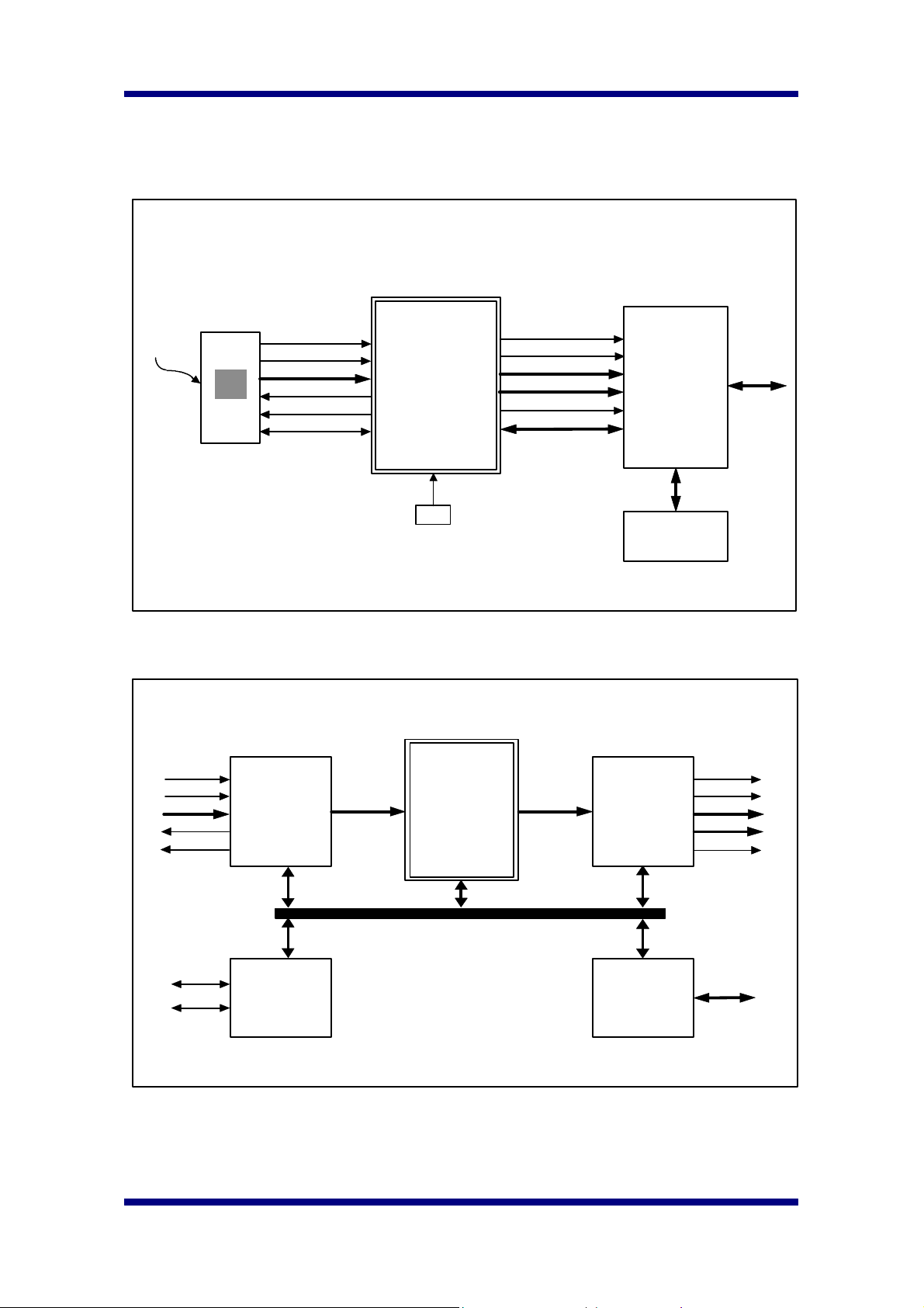
Controller
Video Buffer
4. System Diagram
HYUNDAI
CMOS Image Sensor
Image
HSYNC
VSYNC
PD[7:0]
PCLK
ENB
Serial Interface
H1A424M167
HYUNDAI ISP
MCLK
HSISP
VSISP
Y[7:0]
UV[7:0]
VCLK
Serial Interface
or Parallel Interface
USB
USB
5. Block Diagram
HSYNC
VSYNC
PD[7:0]
PCLK
ENB
SDA
SCK
Video
Input
Interface
Serial
Interface
Master
(to CIS)
Video
Processing
Engine
DRAM
Video
Ouput
Interface
MCU
Interface
( Serial or
Parallel )
HSISP
VSISP
Y[7:0]
UV[7:0]
VCLK
Serial Interface or
Parallel Interface
1999 October 11 Page 10
Hyundai Electronics Industries Co., Ltd. H1A424M167
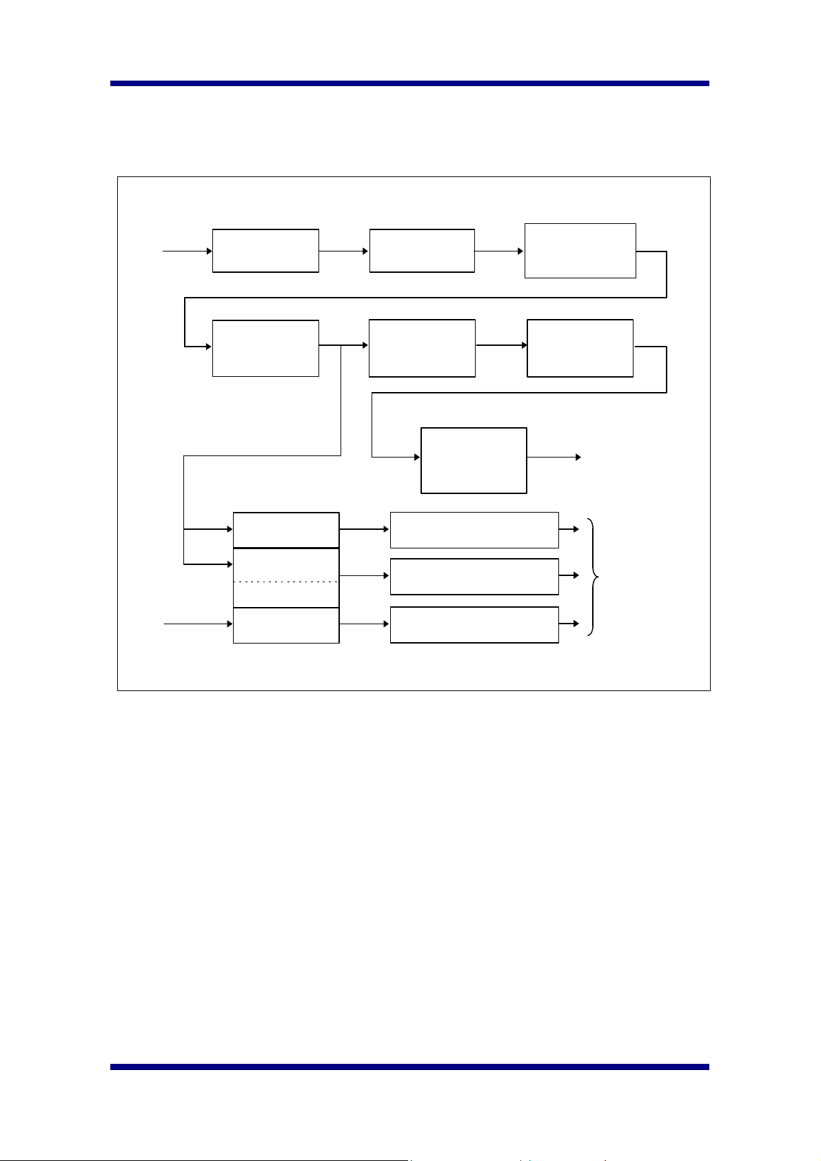
6. Video Processing Engine Block Diagram
Bayer format
RGB Stream
Interpolation
to 24bit RGB
Color
Correction
Gamma
Correction
Reset Level
Offset Data
YCrCb
Y
Color Space
Conversion
Auto White
Balance
Auto Exposure
Anti Flicker
Auto Reset
Level
Histogram
Equalization
Format
conversion
RGB Analog gain control
Integration Time Setting
Reset Level Setting
Edge
Enhnacement
YCrCb
Output Stream
To CIS
1999 October 11 Page 11
Hyundai Electronics Industries Co., Ltd. H1A424M167
7. Functional Description
7.1. Host Interface
Hyundai ISP chip supports two kinds of host interface, serial and 8bit parallel, to
program ISP registers or to read ISP registers. And the host interface is also used to
write or to read CMOS Image Sensor(CIS) registers through ISP.
7.1.1. Serial Interface
The serial interface of Image Signal Processor[ISP] is implemented by the following
pins.
SCLK: Serial Clock SDATA: Serial Data
7.1.1.1. WRITE OPERATION
Write transaction between the ISP and a host is the similar as the well-known I2C serial
interface except that only one byte transfer at each transaction is allowed. The
transaction consists of START CONDITION, DEVICE ADDR + R/W[0], SUB ADDR,
WRITE DATA, and STOP CONDITION states. The single write access sequence is as
follows.
S DEVICE ADDR A1 SUB ADDR A2 WRITE DATA A3 P
[ S ] Operation start condition
[ DEVICE ADDR ] ISP 40h(010_0000 + 0), CIS 22h(001_0001 + 0)
ð device address + R/W bit
[ A1 ] Acknowledge from ISP
[ SUB ADDR ] ISP Sub address space 80h ~ FFh
CIS Sub address space 00h ~ 7Fh
[ A2 ] Acknowledge from ISP
[ WRITE DATA ] Register Value from host
[ A3 ] Acknowledge from ISP
[ P ] Operation stop condition
7.1.1.2. READ OPERATION
Read transaction between the ISP and a host proceeds as the following sequence.
START CONDITION ð DEVICE ADDR + R/W[0] ð SUB ADDR ð START
CONDITION ð DEVICE ADDR + R/W[1] ð READ DATA ð STOP CONDITION
The ISP register access throughput is one byte at each read transaction. But the
1999 October 11 Page 12
Hyundai Electronics Industries Co., Ltd. H1A424M167
CMOS Image Sensor register access through the ISP chip needs two sequential read
operations to compensate the read access delay from CMOS Image Sensor to ISP.
The second read data for the CMOS image sensor register should be recognized as
the right value of the accessed register. But when the ISP auto functions are enabled,
there will be a variable delay for the right data transfer from the CMOS image sensor to
the ISP at the first read access, so the second read access may not get acknowledge
from the ISP until the first read access is completely processed in the ISP. To take care
of the said situation, a system host should repeat the second read access until it get
acknowledge from the ISP or there should be sufficient delay between two accesses.
To summarize, the ISP general register read access is always completed by only one
read transaction, and the CMOS image sensor register access needs two fully
acknowledged read transactions and the last read data is the right value for the
accessed register.
The single read access sequence is as follows.
S1 DADDR 1 A1 SADDR A2 S2 DADDR 2 A3 READ DATA A4 P
[ S1 ] Start condition
[ DADDR 1 ] Device Address ISP 40h(010_0000 + 0),
CIS 22h(001_0001 + 0)
ð device address + R/W bit
[ A1 ] Acknowledge from ISP
[ SADDR ] ISP Sub address space 80h ~ FFh
CIS Sub address space 00h ~ 7Fh
[ A2 ] Acknowledge from ISP
[ S2 ] Start condition
[ DADDR 2 ] Device Address ISP 41h(010_0000 + 1),
CIS 23h(001_0001 + 1)
ð device address + R/W bit
[ A3 ] Acknowledge from ISP
[ READ DATA ] Register Value from ISP
[ A4 ] Acknowledge from HOST
[ P ] Stop condition
* Note ( Importance ! )
ISP General Register Read : 1 Read Operation needed.
CIS Register Read : 2 Read Operation needed, valid data at second read operation.
ISP recognize CIS read command at first read.
1999 October 11 Page 13
Hyundai Electronics Industries Co., Ltd. H1A424M167
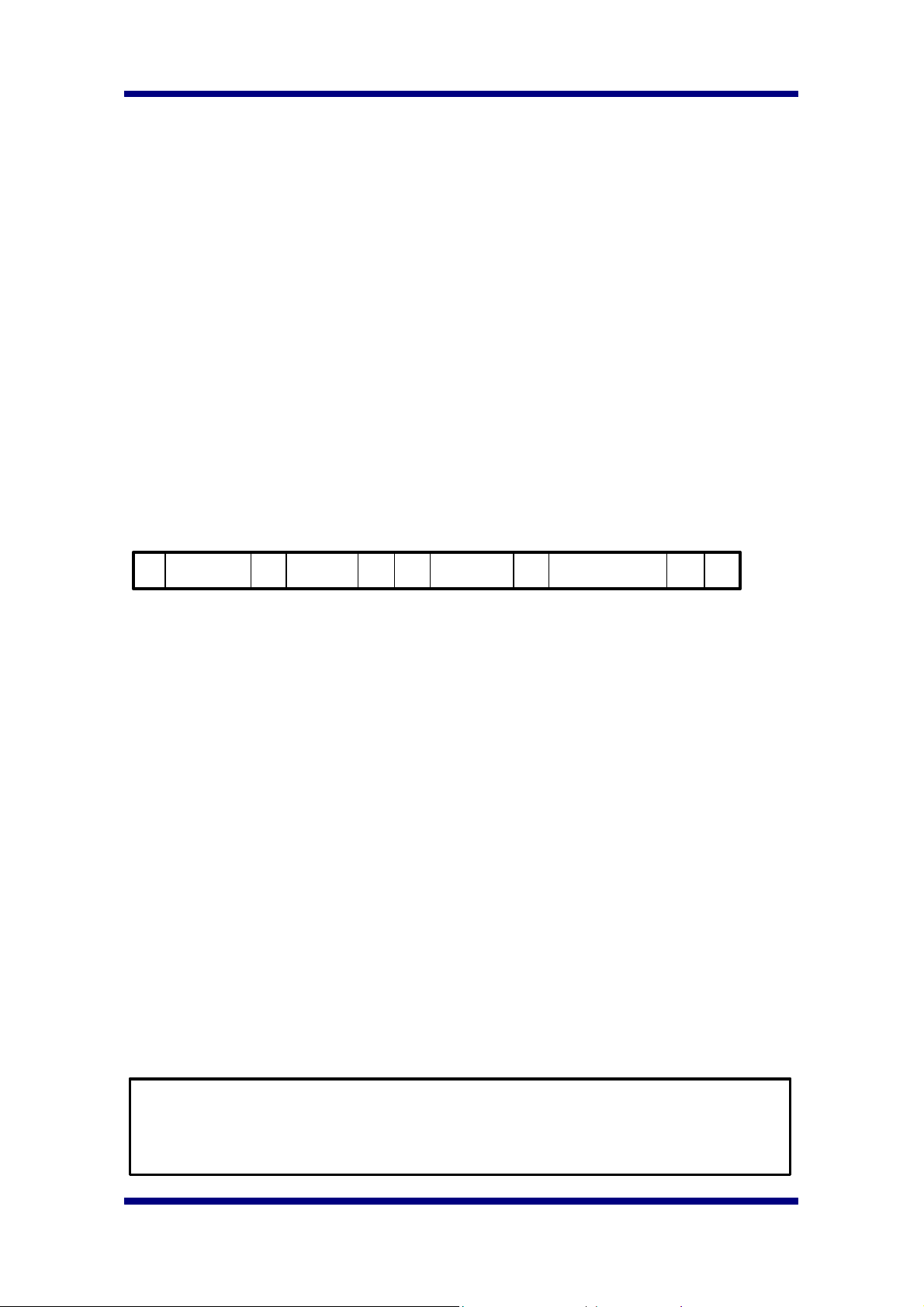
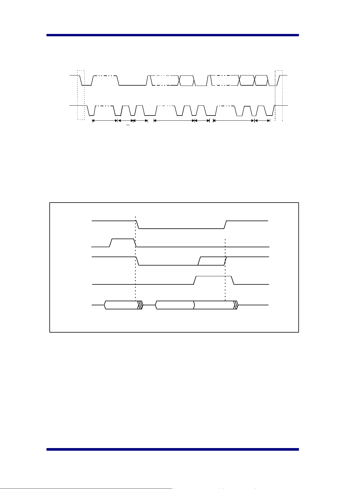
7.1.1.3. Data Transfer Timing on the serial Interface
SDA
SCL
S
START
CONDITION
1-7
1-7
ADDRESS
ADDRESS
8 9
8 9
R/W
R/W
ACK
ACK
1-7
DATA
8 9
ACK
1-7
DATA
8 9
ACK
P
STOP
CONDITION
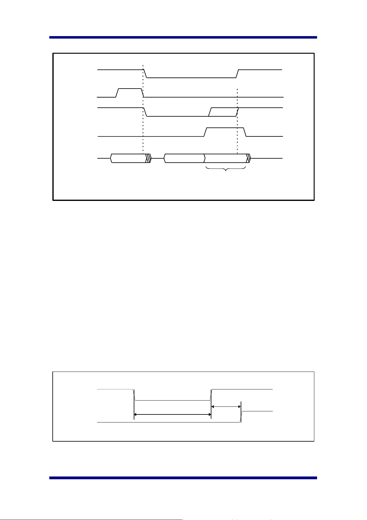
7.1.2. Host Parallel Interface
H1A424M167 ISP supports an external 8-bit microcontroller interface to access
H1A424M167 internal registers.
Basically, the data transfer operations(8bits) are multiplexed on the address bus.
CSB
ALE
IOR
Stretched
IODone
AD[7:0]
A[7:0] D[7:0]
Valid D[7:0]
Host Parallel Read Operation
A Parallel read operation always needs only 1 read cycle different from the serial read
operation. But the host must watch ‘ IODone’ signal for a proper read operation. IODone
signal indicates the completion of read/write operation. So the host must hold the IOR,
CSB signals until IODone signal is active, to read the valid data on AD[7:0] lines. At the
final stage, the host ends the bus cycle(CSB, IOR) then IODone signal become
inactive.
1999 October 11 Page 14
Hyundai Electronics Industries Co., Ltd. H1A424M167
IOW
CSB
Host Parallel Write Operation
ALE
Stretched
IODone
AD[7:0]
A[7:0] D[7:0]
Stretched
Active write operation
Similar to parallel read operation, parallel write operation needs only 1 operation cycle.
The host must watch ‘ IODone’ signal for a proper write operation. IODone signal
indicates the completion of read/write operation. So the host must hold the IOW, CSB,
Write Data[7:0] signals until IODone signal become active. When IODone signal
become active, ISP accept the write data internally. At the final stage, the host ends the
bus cycle(CSB, IOW, Write Data[7:0]) and IODone signal become inactive.
ISP holds IODone active until read/write operation is completed. CIS register read/write
operation needs more time than ISP register read/write operation. So IODone active
signal for CIS register read/write operation is much longer than that of ISP register
read/write operation.
7.1.3. Serial or Parallel Interface selection
The selection between serial interface and parallel interface is made at hardware reset
time. If CSB/MODE pin, pin number 64, is pulled down during reset, Serial Interface is
configured, and otherwise parallel interface is selected.
For example, Serial Interface selection timing is as below.
RESETB
CSB/MODE
1999 October 11 Page 15
More than 64 MCLK
Serial Interface Selection
 Loading...