

HEI GMS84524T, GMS84524, GMS84512T, GMS84512 Datasheet

Rev. 2.1NOV. 1996
USER’S MANUAL
HYUNDAI MicroElectronics
GMS84512 / 84524
8-BIT SINGLE CHIP MICROCOMPUTER

GMS84512/84524 USER’ S MANUAL
Table of Contents
1. Overview
2. CPU
3. Peripheral Function
4. Control Function
5. Support Tool
6. Appendix

1. Overview
1. Features
2. Block Diagram
3. Summary Of Peripheral Function Register
4. Pin Assignment
5. Pin Description
6. Terminal Types
2. CPU
1. Registers
2. Memory Space
3. Peripheral Function
1. PORT
2. Clock Generation Circuit
3. Timer
4. A/D Comparator
5. Serial I/O
6. PWM
7. Interrupt Interval Measurement Circuit
8. On Screen Display
4. Control Function
1. Interrupts
2. Standby Function
3. Reset Function
5. Support Tool
1. Emulator
2. Debugger
3. Assembler
4. Linker
5. Font Editor
6. OTP Chip
6. Appendix
l Electrical Data
l Package Outline

GMS 84512 / 84524
1 - 1
An 8-bit microcomputer using the G8MC Core is a single-chip microcomputer including several peripheral
functions such as Timer, I/O Comparator, Serial I/O, PWM, Watch-dog Timer and On-Screen Display.
1.1 FEATURES
l ROM 12,288 Bytes ( GMS84512 ) 24,576Bytes ( GMS84524 )
l RAM 256 Bytes
l Minimum instruction execution time1 us ( @ Xin = 4 MHz )
l I/O PORT 42 ( INPUT: 3, OUTPUT: 10, I/O: 29 )
l Serial I/O 8-bit X1 ch. ( 1MHz, 500KHz, 250 KHz, Ext. clock )
l A/D Comparator 5-bit X4 ch. ( max. 1 LSB )
l Pulse Width Modulation 14-bit X1 ch.
7-bit X8 ch.
l Timer
- Timer/Counter 8 bit X4 ch. ( 16-bit X2 ch is Acceptable)
- Basic Interval Timer 8 bit X1 ch.
- Watch Dog Timer
l Interrupt Interval estimation circuit for Remocon signal receiving
l Interrupt Sources 14 sources
l Pulse ( T2048 ) Output Function Period : 2,048 us, Duty: 50 %
l On Screen Display
- Kinds of character 128 kinds (include 2 test characters)
- Construction of character 14 dots X18 dots
- Size of character 4 X4 kinds
- Number of display character 22 Characters X3 lines ( Max. 12 lines)
- Display colors 8 kinds
- Color Edge, Smoothing Function
l Power Save Mode STOP mode
l Operating Voltage 4.5 ~5.5 V
l Package 52 SDIP
l
OTP chip GMS84512T/84524T
GMS 84512 / 84524
1 - 2
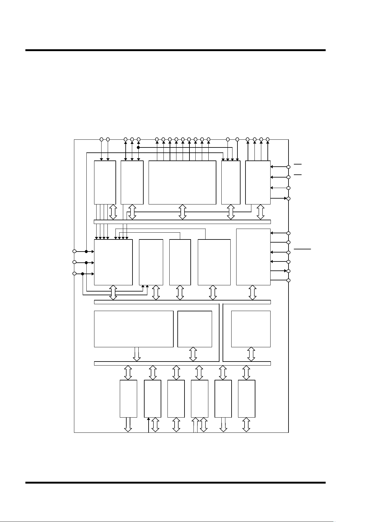
1.2 BLOCK DIAGRAM
R40 ~ R45
G8MC
CORE
R20 ~ R27
R2 PORT
R32 ~ R37
R3 PORT
R00 ~ R07
R0 PORT
R10 ~ R16
R1 PORT
R50 ~ R53
R5 PORT
PWM
A/D COMP.
R53/ Y
R52/ B
R50/ R
R51/ G
R15/ Cin1
R16/ Cin2
R43/ PWM2
R42/ PWM3
R45/ PWM0
R44/ PWM1
R37/ PWM6
R36/ PWM7
R41/ PWM4
R40/ PWM5
R32/ PWM8
R26/ EC2
R27/ EC3
R33/ Sout
R35/ Sin/ Cin3
R34/ Sclk
INTERRUPT
CONTROLLER
REMOCON
TIMER
SERIAL
I/O
CLOCK GEN./
SYSTEM CON.
OSD
R30/ INT1
R31/ INT2
HD
VD
R17/ Cin0/ INT3
OSC2
OSC1
Vdd
TEST
Xin
RESET
Vss
Xout
RAM
( 256 byte )
WATCH DOG
TIMER
R30 ~ R31
R17
R4 PORT
ROM
( 12K / 24K)
PRESCALER
/ B.I.T.
GMS 84512 / 84524
1 - 3
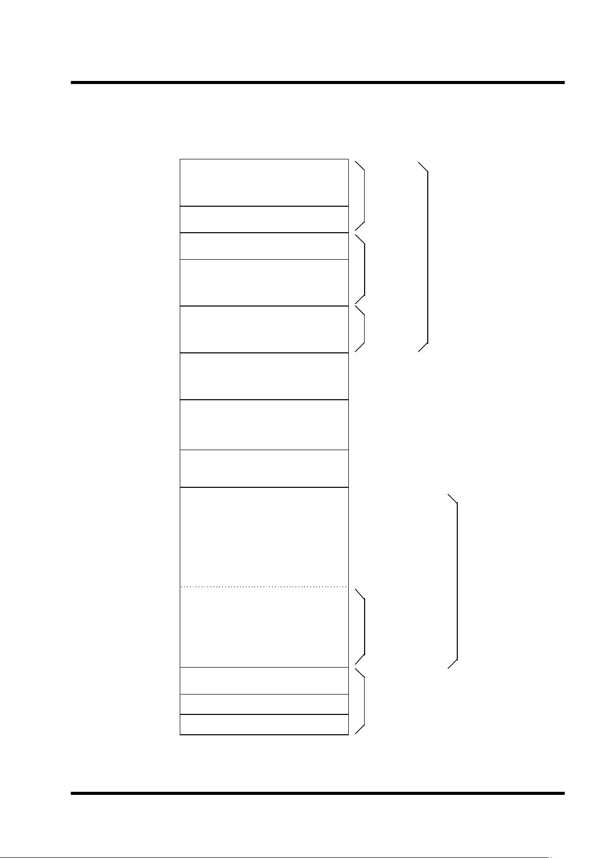
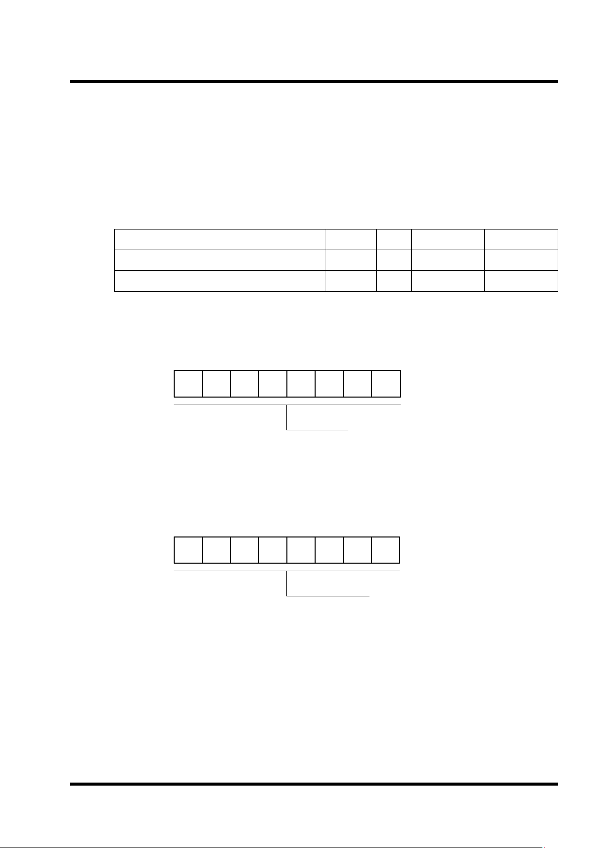
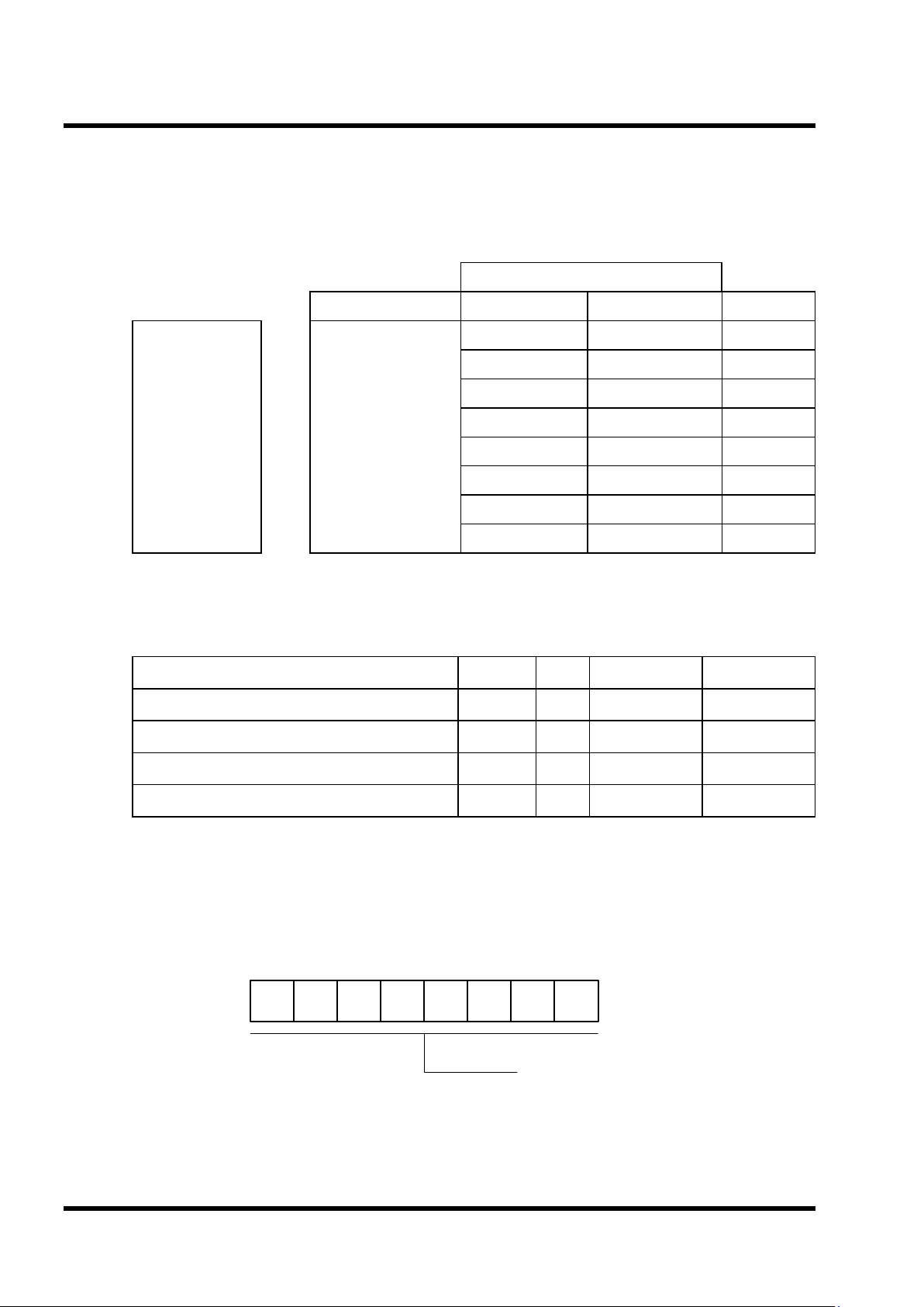
1.2 Peripheral Function Overview
BLOCK
Function
INDEX
PRESCALER
/ B.I.T.
Prescaler is consists of 10 bits binary counter, and divide oscillation clock.
The divided output from each bit of prescaler provided to peripheral hardware.
B.I.T a 8 bit binary counter has a function such as security of oscillation
stabilization time, generation of basic interval time interrupt as watch function,
providing the clock for watch-dog timer
3 - 13
WATCH-DOG
-TIMER
WDT is consist of 6-bit binary counter, WDTR(Watch-Dog Timer Register), and
comparator, input clock of WDT is provided by Basic Interval Timer interrupt
and maximum output cycle is 4 seconds.
When WDTOM is ‘1’, the output of WDT reset the Device.
3 -16
TIMER /
COUNTER
Timer is an 8 bit binary counter and consisted of T0, T1, T2, T3.
As an 8-bit binary counter, each T0, T1 can be used 16-bit interval Timer to
connect each other. As an 8 bit binary counter/event counter each T2, T3 can
be used 16-bit/event counter to connect each other.
At 4 MHz oscillation, Maximum interval time of T0 is 8.192 ms, T1 is 2048 ms,
T0-T1 is about 2 seconds, T2 is 2.048 ms, T3 is 512uS,T2-T3 is about 0.5
seconds
3 - 19
A/D COMP ARATOR
A/D Comparator has 5 bit resolution, and 4 input channel. It has sample and
hold function of input. At 4 MHz it takes about 8uS to compare. Error is less
than 1/2 LSB.
3 - 26
SERIAL I/O
It is 8 bit clock synchronous serial interface unit, the clock transmission cycle is
1uS,2uS,4uS Which can be selected external clock. When IOSW(Bit 6 Of
Serial I/O Mode Register) is ‘1’, R33 pin operates Sout at transmission mode,
Sin at receiving mode.
3 - 28
PWM
( Pulse Width
Modulation )
PWM is consists of 14 bit PWM 1 ch and 7 bit PWM 8 ch.
14 bit PWM has 0.5uS minimum resolution width, 8192uS cycle time, 7 bit
PWM has 8uS minimum resolution 8uS,1024uS, cycle time. The polarity of
PWM output can be assign by Software.
3 - 32
INTERRUPT
INTERVAL
MEASUREMENT CIRCUIT
Interrupt interval measurement circuit consists of 8 bit binary counter, interrupt
interval saving circuit. It can select 32uS, 64uS as a measurement clock .
Because it can select external signal edge, measurement of input signal cycle
or pulse width is possible. So it can be used Remocon receiving.
3 - 38
OSD
( On-Screen Display )
Maximum number of character or symbol displayed in CRT is 128 basically
displayed by 22 charactersX3 lines. Maximum 12 lines is possible with OSD
interrupt.
OSD clock can use 4 MHz ~ 8 MHz size of display character is 16 kinds, it can
be used by line unit. The color of display character is 8 kinds it can be used by
character unit. In display mode, there are character mode, background mode,
color mode, and Blanking mode, it can be used by line unit especially
smoothing function and OSD oscillator control function exists.
3 - 41
GMS 84512 / 84524
1 - 4
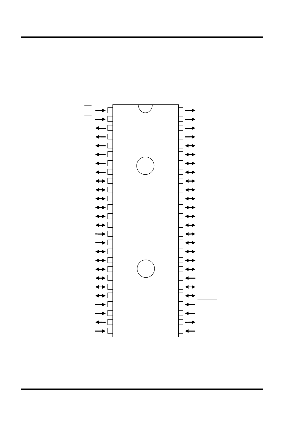
1.4 PIN ASSIGNMENT
1
HD
52
R50/ R
2
VD
51
R51/ G
3
R45/ PWM0
50
R52/ B
4
R44/ PWM1
49
R53/ Y
5
R43/ PWM2
48
R00
6
R42/ PWM3
47
R01
7
R41/ PWM4
46
R02
8
R40/ PWM5
45
R03
9
R37/ PWM6
44
R04
10
R36/ PWM7
43
R05
11
R35/ Sin/ Cin3
42
R06
12
R34/ Sclk
41
R07
13
R33/ Sout
40
R10
14
R32/ PWM8
39
R11
15
R31/ INT2
38
R12
16
R30/ INT1
37
R13
17
R27/ EC3
36
R14
18
R26/ EC2
35
R15/ Cin1
19
R25/ T2048
34
R16/ Cin2
20
R24
33
R17/ Cin0/ INT3
21
R23
32
R20
22
R22
31
R21
23
TEST
30
RESET
24
Xin
29
OSC1
25
Xout
28
OSC2
26
Vss
27
Vdd
HME
GMS84512/84524
GMS 84512 / 84524
1 - 5
1.5 PIN DESCRIPTION
Classification No.
Symbol
I/O Function Type Remark
Power
27 Vdd Input Power supply (4.5~5.5V)
26 Vss Input Ground (0V)
System
23 TEST Input TEST Input pin
Control or
At 'L' input: SINGLE CHIP MODE
IA
Clock
At 'H' input : TEST MODE
24 Xin Input CRYSTAL connection pin (with Xout)
If an external clock is used, Xin pin should be
connected external clock source
25 Xout Output CRYSTAL connection pin(with Xin)
If an external clock used, Xout pin
should be open
30 RESET Input In the state of 'L' level, system
IA
enter the reset state
OSD
1 HD Input Horizontal synchronizing signal input pin
IA
2 VD Input Vertical synchronizing signal input pin
28 OSC2 Ouptut Clock output for OSD
29 OSC1 Input Clock input for OSD
49 Y Output Switching signal output pin R53 share
50 B Output BLUE signal output pin
OA
R52 share
51 G Output GREEN signal output pin R51 share
52 R Output RED signal output pin R50 share
PWM
3 PWM0 Output Pulse width modulation output pin R45 share
4 PWM1 Output (7BIT PWM) R44 share
5 PWM2 Output
OB
R43 share
6 PWM3 Output R42 share
7 PWM4 Output R41 share
8 PWM5 Output R40 share
9 PWM6 Output
IOF
R37 share
10 PWM7 Output R36 share
14 PWM8 Output 14BIT PWM output pin
IOD
R32 share
19 T2048 Output Pulse(2048uS) output pin R25 share
SCI
11 Sin Input Serial Data Input pin
IOE
R35 share
12 Sclk I/O Serial Clock I/O pin
IOG
R34 share
13 Sout Output Serial Data output pin R33 share
TIMER
17 EC3 Input Event Counter input pin
IOB
R27 share
GMS 84512 / 84524
1 - 6
Classification NO.
Symbol
I/O Function
TYPE
Remarks
Interrupt
15 INT2 Input External interrupt request input pin
IB
R31 share
16 INT1 Input (INT1,INT2 : Remocon input capture R30 share
33 INT3 Input Input possible)
IC
R17 share
A/D
11 Cin3 Input Analog input pin
IOE
R35 share
Comparator
33 Cin0 Input (Default selection : Cin0)
IC
R17 share
34 Cin2 Input
IOC
R16 share
35 Cin1 Input R15 share
I/O Port
41 R07 I/O R0 Port
~
~
(Can assigned I/O state bit by bit by R0DD)
IOA
48 R00 I/O
33 R17 Input R1 Port ( R17 Input only )
IC
Cin0/INT3 share
34 R16 I/O ( 7 ports of R10~R16 can assigned I/O
IOC
Cin2 shrae
~
~
state bit by bit by R1DD Cin1 share
40 R10 I/O
IOA
17 R27 I/O R2 Port
IOB
EC3 share
18 R26 I/O ( Can assigned I/O state bit by bit EC2 share
19 R25 I/O by R2DD)
IOD
T2048 share
20 R24 I/O
21 R23 I/O
22 R22 I/O
IOA
31 R21 I/O
32 R20 I/O
9 R37 I/O R3 PORT
IOB
PWM6 share
10 R36 I/O ( 6 Bits of R31~R32 can assigned I/O PWM7 share
11 R35 I/O state bit by bit by R3DD
IOE
Sin/Cin3 share
12 R34 I/O
IOG
Sclk share
13 R33 I/O Sout share
14 R32 I/O
IOD
PWM8 share
15 R31 Input ( R30,R31 is input only)
IB
INT2 share
16 R30 Input INT1 share
3 R45 Output R4 Port PWM0 share
4 R44 Output ( 6 bit output only ) PWM1 share
5 R43 Output
OB
PWM2 share
6 R42 Output PWM3 share
7 R41 Output PWM4 share
8 R40 Output PWM5 share
49 R53 Output R5 Port Y share
50 R52 Output ( 4 bit output only )
OA
B share
51 R51 Output G share
52 R50 Output R share
GMS 84512 / 84524
1 - 7
1.6 TERMINAL TYPES
PIN TERMINAL TYPE at RESET
Xin
Xout
Oscillation
OSC1
OSC2
Oscillation
Stop
RESET
HD
VD
TEST
( “L” )
Hi-Z
R30/ INT1
R31/ INT2 Hi-Z
R17/ Cin0
/ INT3 Hi-Z
IA type
IB type
INT1,INT2
Data Bus
I
Vdd
Vss
Rd
SCHMITT Input
IC type
INT1,INT2
Data Bus
I
Vdd
Vss
Rd
SCHMITT Input
Cin3
Test Pin is using normal
gate
SCHMITT Input
RST
H Sync
V sync
I
Vdd
Vss
Vss
Xin
Xout
Vdd
Vdd
Vss
Vdd
Vss
OSDON
Vss
Vss
Xin
Xout
Vdd
Vss
Vdd
Vss
Vdd
Vss
STOP
Vss
GMS 84512 / 84524
1 - 8
PIN TERMINAL TYPE at RESET
R50/ R
R51/ G
R52/ B
R53/ Y
Hi-Z
R45/ PWM0
R44/ PWM1
R43/ PWM2
R42/ PWM3
R41/ PWM4
R40/ PWM5
Hi-Z
R00~R07
R10~R14
R20~R24
Hi-Z
R26/ EC2
R27/ EC3
Hi-Z
OA type
OB type
IOA type
IOB type
Data REG.
Data Bus
PWM0¡-PWM5
Vss
Selection
MUX
O
Vss
Vdd
Vss
Vdd
Vss
Data Bus
R, G, B, Y
Selection
MUX O
Data REG.
Data Bus
Vss
Vdd
Vss
Data Bus
MUX
IO
Direction REG.
Vdd
Data Bus
Data REG.
Rd
EC2, EC3
SCHMITT input
Data Bus
Vss
Vdd
Vss
Data Bus
MUX
IO
Direction REG.
Vdd
Data Bus
Data REG.
Rd
GMS 84512 / 84524
1 - 9
PIN TERMINAL TYPE at RESET
R15/ Cin1
R16/ Cin2
Hi-Z
R25/ T2048
R32/ PWM8 Hi-Z
R35/ Sin
/ Cin4
Hi-Z
IOC type
IOD type
IOE type
Cin1, Cin2
Data Bus
Vss
Vdd
Vss
Data Bus
MUX
IO
Direction REG.
Vdd
Data Bus
Data REG.
Rd
Rd
Data Bus
Vss
Vdd
Vss
Data Bus
MUX
MUX
IO
Vdd
Selection
T2048, PWM8
Data Bus
Data REG.
Direction REG.
Sin
Data Bus
Vss
Vdd
Vss
Data Bus
MUX
IO
Vdd
Selection
Data Bus
Data REG.
SCHMITT input
Direction REG.
Rd
Cin4
GMS 84512 / 84524
1 - 10
PIN TERMINAL TYPE at RESET
R36/ PWM7
R37/ PWM6
Hi-Z
R34/ Sclk
R33/ Sout
Hi-Z
Data Bus
IOF type
IOG type
MUX
SCHMITT input
Rd
Rd
Data Bus
Vss
Vss
Data Bus
MUX
IO
Selection
PWM6,PWM7
Data Bus
Data REG.
Direction REG.
MUX
Vss
Vss
Data Bus
IO
Selection
PWM6,PWM7
Data Bus
Data REG.
Direction REG.
MUX

GMS84512/84524 USER’ S MANUAL
Table of Contents
1. Overview
2. CPU
3. Peripheral Function
4. Control Function
5. Support Tool
6. Appendix
GMS 84512 / 84524
2 - 1
2.1. REGISTERS
Program Counter
15 8
PCH
7 0
PCL
A - Register
7 0
A
15 8
Y
( YA 16bit Accumulator )
7 0
A
X - Register
7 0
X
Y - Register
7 0
Y
Program Status Word
7 0
PSW
Stack Pointer *1
7 0
SP
Carry Flag
Z CH IG BN V
Zero Flag
Interrupt Enable Flag
Half Carry Flag
Break Flag
G ( Direct Page ) Flag
Overflow Flag
Negative Flag
15 8
*1 STACK ADDRESS ( 0100H~-013FH )
01
H
Hardware fixed
7 0
SP

GMS 84512 / 84524
2 - 2
2.1.1. A - Register
l 8 bit Accumulator
l In the case of 16-bit operation, compose the lower 8-bit of YA (16-bit Accumulator)
l In the case of multiplication instruction, execute as a multiplier register.
After multiplication operation, the lower 8-bit of the result enters. (Y * A → YA)
l In the case of division instruction, execute as the lower 8-bit of dividend.
After division operation, quotient enters. (YA ¡À X ¡æ Q: A , R: Y )
2.1.2. X- Register
l General-purpose 8-bit register
l In the case of index addressing mode within direct page(RAM area), execute as index
register
l In the case of G mode operation, execute as destination address register.
The operation result enters into memory indirectly addressed by X register.
l In the case of division instruction, execute as divisor register.
2.1.3. Y- Register
l General-purpose 8-bit register
l In the case of index addressing mode, execute as index register
l In the case of 16-bit operation instruction, execute as the upper 8-bit of YA (16-bit
accumulator).
l In the case of multiplication instruction, execute as a multiplicand register.
After multiplication operation, the upper 8-bit of the result enters.
l In the case of division instruction, execute as the upper 8-bit of dividend.
After division operation, quotient enters.
l Can be used as loop counter of conditional branch command. (e.g. DBNE Y, REL)
2.1.4. Stack Pointer
l In the cases of subroutine call, Interrupt and PUSH, POP, RETI, RET instruction,
stack data on RAM or in the case of returning, assign the storage location having
stacked data.
l Stack area is constrained within 1-page (00H-FFH). Page is fixed by H/W. User can
only assign the lower address. At the initial stage, stack pointer should be initialized to
GMS 84512 / 84524
2 - 3
point to RAM area having H/W.
¨çInterrupt
¨èRETI
¨éSubroutine CALL
¨êRET
¨ëPUSH A ( X, Y, PSW )
¨ìPOP A ( X, Y, PSW )
M (sp) ¡ç ( PCH )
sp ¡ç sp - 1
M (sp) ¡ç PCL )
sp ¡ç sp - 1
M (sp) ¡ç A
M (sp) ¡ç ( PCH )
sp ¡ç sp - 1
M (sp) ¡ç ( PCL )
sp ¡ç sp - 1
M (sp) ¡ç ( PSW )
sp ¡ç sp - 1
sp ¡ç sp - 1
sp ¡ç sp + 1
( PCL ) ¡ç M (sp)
sp ¡ç sp + 1
( PCH) ¡ç M (sp)
sp ¡ç sp + 1
A ¡ç M (sp)
( PSW ) ¡ç M (sp)
sp ¡ç sp + 1
( PCL ) ¡ç M (sp)
sp ¡ç sp + 1
( PCH) ¡ç M (sp)
sp ¡ç sp + 1

GMS 84512 / 84524
2 - 4
2.1.5. Program Counter ( PC )
l Program counter is a 16-bit counter consisted of 8-bit register PCH and PCL.
l Addressing space is 64K bytes.
l In reset state, Reset routine address in address FFFFH and FFFEH enter into PC.
2.1.6. Program Status Word( PSW )
l PSW is an 8-bit register.
l Consisted of the flags to show the post state of operation and the flags determining
the CPU operation, initialized as 00H in reset state.
PSW
¨çCarry Flag ( C )
l After operation, set when there is a carry from bit7 of ALU or there is not a borrow.
l Set by SETC and clear by CLRC.
l Executable as 1-bit accumulator.
l Branch condition flag of BCS, BCC.
¨èZero Flag ( Z )
l After operation also including 16-bit operation, set if the result is “0”.
l Branch condition flag of BEQ, BNE.
¨éInterrupt Enable Flag ( I )
l Master enable flag of interrupt except for RST(reset).
l Set and cleared by EI, DI .
¨êHalf Carry Flag ( H )
l After operation, set when there is a carry from bit3 of ALU or there is not a borrow
from bit4 of ALU.
l Can not be set by any instruction.
l Cleared by CLRV instruction like V flag.
7
N6V5G4B3H
2
I
1
Z0C
GMS 84512 / 84524
2 - 5
¨ëBreak Flag ( B )
l Set by BRK (S/W interrupt) instruction to distinguish BRK and TCALL instruction
having the same vector address.
¨ìDirect Page Flag ( G )
l Assign direct page (0-page, 1-page).
l Set and cleared by SETG, CLRG instruction.
l If used with PG2R(00FC
H
) it is enable to access 2-page ( OSD RAM ).
G-flag PG2R Direct Page
0 -
0 - Page Access
1 0
1 - Page Access
1
2 - Page Access
*NOTICE : Always after clearing, PG2R is enable to be accessed for it is the register
of 0-page
¨íOverflow Flag ( V )
l After operation, set when overflow or underflow occurs.
l In the case of BIT instruction, bit6 of memory location is input to V-flag.
l Cleared by CLRV instruction, but not set by any instruction.
l Branch condition flag of BVS, BVC.
¨îNegative Flag ( N )
l N-flag is set whenever the result of a data transfer or operation is negative (bit7 isset to “1”).
l In the case of BIT instruction, bit7 of memory location is inputted to N-flag
l No CLEAR and SET instruction.
l Branch condition flag of BPL, BMI.

GMS 84512 / 84524
2 - 6
2.2 MEMORY SPACE
The memory space of GMS84512/84524 is 64K byte, it is equipped with RAM area, OSD RAM
area, FONT ROM area and PROGRAM ROM area.
2.2.1. RAM area
0-PAGE ( 0000
H
- ~ 00FFH )
RAM 192 Bytes ( 0000
H
~ 00BFH ) and peripheral function register( 00C0H ~ 00FFH )
1-PAGE ( 0100
H
~ 013FH )
RAM 64 Bytes ( 0100
H
~ 013FH ) and STACK area
2-PAGE ( 0200
H
~ 02D5H )
OSD RAM 182 Bytes ( 0200
H
~ 02D5H )
2.2.2. FONT ROM area ( 2000
H
~
3FFFH )
128 character OSD FONT
2.2.3. PROGRAM ROM area
Approximately ROM memory is 12 K bytes and it is domain of User Program.
The highest page(FF00
H
~ FFFFH ) is called U- Page and it is utilized domain as following.
PCALL area ( FF00
H
~ FFBFH )
Domain of jumping at PCALL instruction
TCALL Vector area ( FFC0
H
~ FFDFH )
Storage domain of vector address at TCALL instruction.
Interrupt Vector area ( FFE0
H
~ FFFFH )
Storage domin of interrupt vector address,inclusive RESET
GMS 84512 / 84524
2 - 7
MEMORY MAP (GMS84512/84524 )
FFFF
H
FFE0
H
FFC0
H
PROGRAM ROM
No H/W
No H/W
INTERRUPT VECTOR AREA
TCALL VECTOR AREA
PCALL AREA
FONT ROM
( 8 K bytes )
OSD RAM
( 182 Bytes )
No H/W
RAM ( STACK ) ( 64 Bytes )
PERIPHERAL REGISTERS
RAM
( 192 Bytes )
FF00
H
A000
H
D000
H
3FFF
H
2000
H
02D5
H
0200
H
013F
H
0100
H
00FF
H
00BF
H
0000
H
0-PAGE
1-PAGE
2-PAGE
DIRECT-PAGE
GMS84524
( 24K Bytes )
GMS84512
( 12K Bytes )
U-PAGE
GMS 84512 / 84524
2 - 8
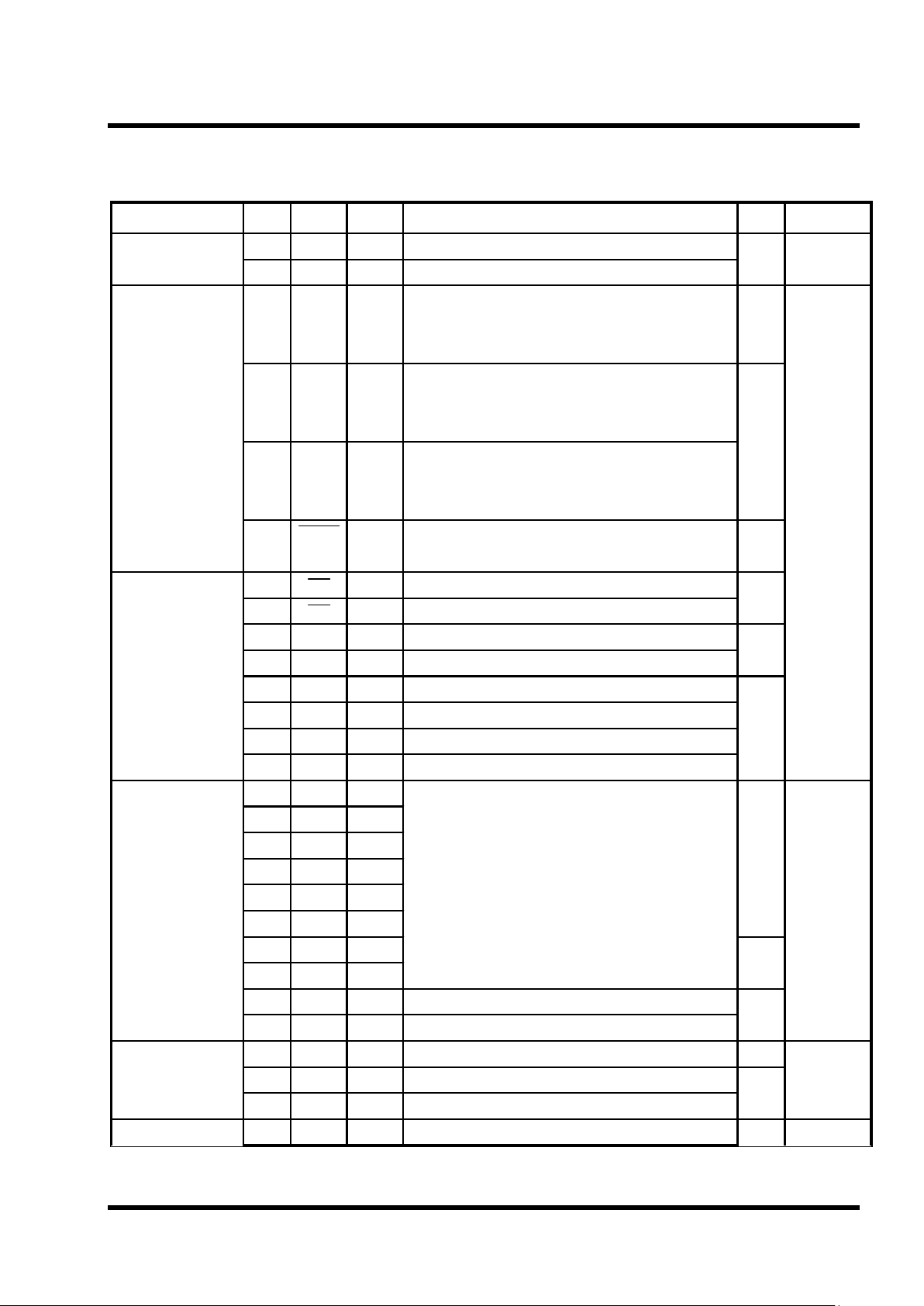
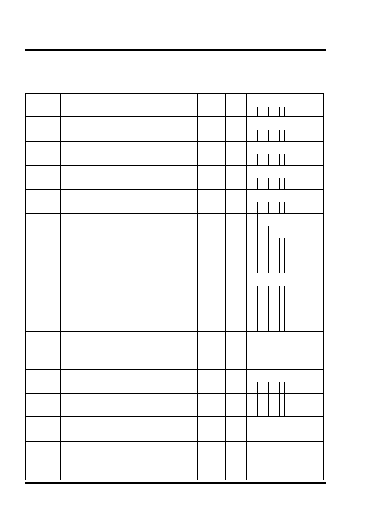
TABLE 2.1. PERIPHERALREGISTER LIST
Address Register Name SYMBOL R/W
RESET VALUE
Page
7 6 5 4 3 2 1 0
00C0
H
R0 PORT DATA REGISTER R0 R/W
Undefined
3 - 1
00C1
H
R0 PORT I/O DIRECTION REGISTER R0DD W 0 0 0 0 0 0 0 0 3 - 1
00C2
H
R1 PORT DATA REGISTER R1 R/W
Undefined
3 - 2
00C3
H
R1 PORT I/O DIRECTION REGISTER R1DD W - 0 0 0 0 0 0 0 3 - 2
00C4
H
R2 PORT DATA REGISTER R2 R/W
Undefined
3 - 4
00C5
H
R2 PORT I/O DIRECTION REGISTER R2DD W 0 0 0 0 0 0 0 0 3 - 4
00C6
H
R3 PORT DATA REGISTER R3 R/W
Undefined
3 - 6
00C7
H
R3 PORT I/O DIRECTION REGISTER R3DD W 0 0 0 0 0 0 - - 3 - 6
00C8
H
R4 PORT DATA REGISTER R4 R/W - -
Undefined
3 - 9
00C9
H
R5 PORT DATA REGISTER R5 R/W - - - - Undefined 3 - 10
00CA
H
PORT FUNCTION SELECTION REGISTER FUNC W - - - 0 0 0 0 0 3 - 3
00CB
H
EXT. INTERRUPT EDGE SELECTION REGISTER IEDS W - - 0 0 0 0 0 0 3 - 39
00CC
H
OPERATION MODE REGISTER TMR W - - - - - 0 0 0
¡ª
00CE
H
BASIC INTERVAL TIMER REGISTER BITR R
Undefined
3 - 16
CLOCK CONTROL REGISTER CKCTLR W - - 0 1 0 1 1 1 3 - 13
00CF
H
WATCH-DOG TIMER REGISTER WDTR W - 0 1 1 1 1 1 1 3 - 17
00D0
H
TIMER MODE REGISTER0 TM0 R/W - 0 0 0 0 0 0 0 3 - 21
00D1
H
TIMER MODE REGISTER2 TM2 R/W - 0 0 0 0 0 0 0 3 - 21
00D2
H
TIMER0 DATA REGISTER TDR0 R/W
Undefined
3 - 21
00D3
H
TIMER1 DATA REGISTER TDR1 R/W
Undefined
3 - 21
00D4
H
TIMER2 DATA REGISTER TDR2 R/W
Undefined
3 - 21
00D5
H
TIMER3 DATA REGISTER TDR3 R/W
Undefined
3 - 21
00D6
H
A/D COMPARATOR MODE REGISTER CMR W *6 0 0 - 0 0 0 0 0 3 - 27
00D7
H
A/D COMP. CHANNEL SELECTION REGISTER CIS W - - - - - - 0 0 3 - 27
00D8
H
SERIAL I/O MODE REGISTER SIOM R/W *0 - 0 0 0 0 0 0 1 3 - 29
00D9
H
SERIAL I/O DATA REGISTER SIOR R/W
Undefined
3 - 28
00DA
H
PWM0 DATA REGISTER PWMR0 W -
Undefined
3 - 35
00DB
H
PWM1 DATA REGISTER PWMR1 W -
Undefined
3 - 35
00DC
H
PWM2 DATA REGISTER PWMR2 W -
Undefined
3 - 35
00DD
H
PWM3 DATA REGISTER PWMR3 W -
Undefined
3 - 35
GMS 84512 / 84524
2 - 9
Address Register Name SYMBOLR/W
RESET VALUE
Page
76543210
00DE
H
PWM4 DATA REGISTER PWMR4 W -
Undefined
3 - 35
00DF
H
PWM5 DATA REGISTER PWMR5 W -
Undefined
3 - 35
00E0
H
PWM6 DATA REGISTER PWMR6 W -
Undefined
3 - 35
00E1
H
PWM7 DATA REGISTER PWMR7 W -
Undefined
3 - 35
00E2
H
PWM8 DATA REGISTER HIGH PWM8H R/W
Undefined
3 - 36
00E3
H
PWM8 DATA REGISTER LOW PWM8L R/W --
Undefined
3 - 36
00E4
H
PWM CONTROL REGISTER1 PWMCR1 R/W 00000000 3 - 37
00E5
H
PWM CONTROL REGISTER2 PWMCR2 R/W ---00000 3 - 37
00E6
H
INTERRUPT MODE REGISTER IMOD R/W --000000 4 - 4
00E8
H
INTERRUPT ENABLE REGISTER LOW IENL R/W 00000-- - 4 - 3
00E9
H
INTERRUPT REQUEST FLAG REGISTER LOW IRQL R/W 00000-- - 4 - 4
00EA
H
INTERRUPT ENABLE REGISTER HIGH IENH R/W 00000000 4 - 3
00EB
H
INTERRUPT REQUEST FLAG REGISTER HIGH IRQH R/W 00000000 4 - 4
00EC
H
INTERRUPT INTERVAL DETERMINATION
CONTROL REGISTER
IDCR R/W -----000 3 - 40
00ED
H
INTERRUPT INTERVAL DETERMINATION REGISTER IDR R 00000000 3 - 38
00F0
H
OSD 1st LINE HORIZONTAL POSITION REGISTER HDP1 W --000000 3 - 47
00F1
H
OSD 2nd LINE HORIZONTAL POSITION REGISTER HDP2 W --000000 3 - 47
00F2
H
OSD 3rd LINE HORIZONTAL POSITION REGISTER HDP3 W --000000 3 - 47
00F3
H
OSD 1st LINE VERTICAL POSITION REGISTER VDP1 W -0000000 3 - 47
00F4
H
OSD 2nd LINE VERTICAL POSITION REGISTER VDP2 W -0000000 3 - 47
00F5
H
OSD 3rd LINE VERTICAL POSITION REGISTER VDP3 W -0000000 3 - 47
00F6
H
OSD 1st LINE DISPLAY MODE, CHARACTER SIZE,
SMOOTHING FUNCTION SELECTION REGISTER
DMSS1 W -0000000 3 - 44
00F7
H
OSD 2nd LINE DISPLAY MODE, CHARACTER SIZE,
SMOOTHING FUNCTION SELECTION REGISTER
DMSS2 W -0000000 3 - 44
00F8
H
OSD 3rd LINE DISPLAY MODE, CHARACTER SIZE,
SMOOTHING FUNCTION SELECTION REGISTER
DMSS3 W -0000000 3 - 44
00F9
H
OSD OUTPUT and BACKGROUND CONTROL
REGISTER
OSDCON1 W 00000000 3 - 48
00FA
H
I/O POLARITY CONTROL and OSD OSCILLATION
CONTROL REGISTER
OSDCON2 W 00000000 3 - 48
00FC
H
OSD RAM ( 2 page ) ACCESSABLE REGISTER PG2R** R/W -------0 3 - 43
¡Ø-: Not used *0: READ only for bit 0 *6: READ only for bit 6
¡Ø Write Only Register can not be accessed by bit manipulation instruction.
** : OSD RAM area (2-page) can be accessed by LDM,SET1
GMS 84512 / 84524
2 - 10
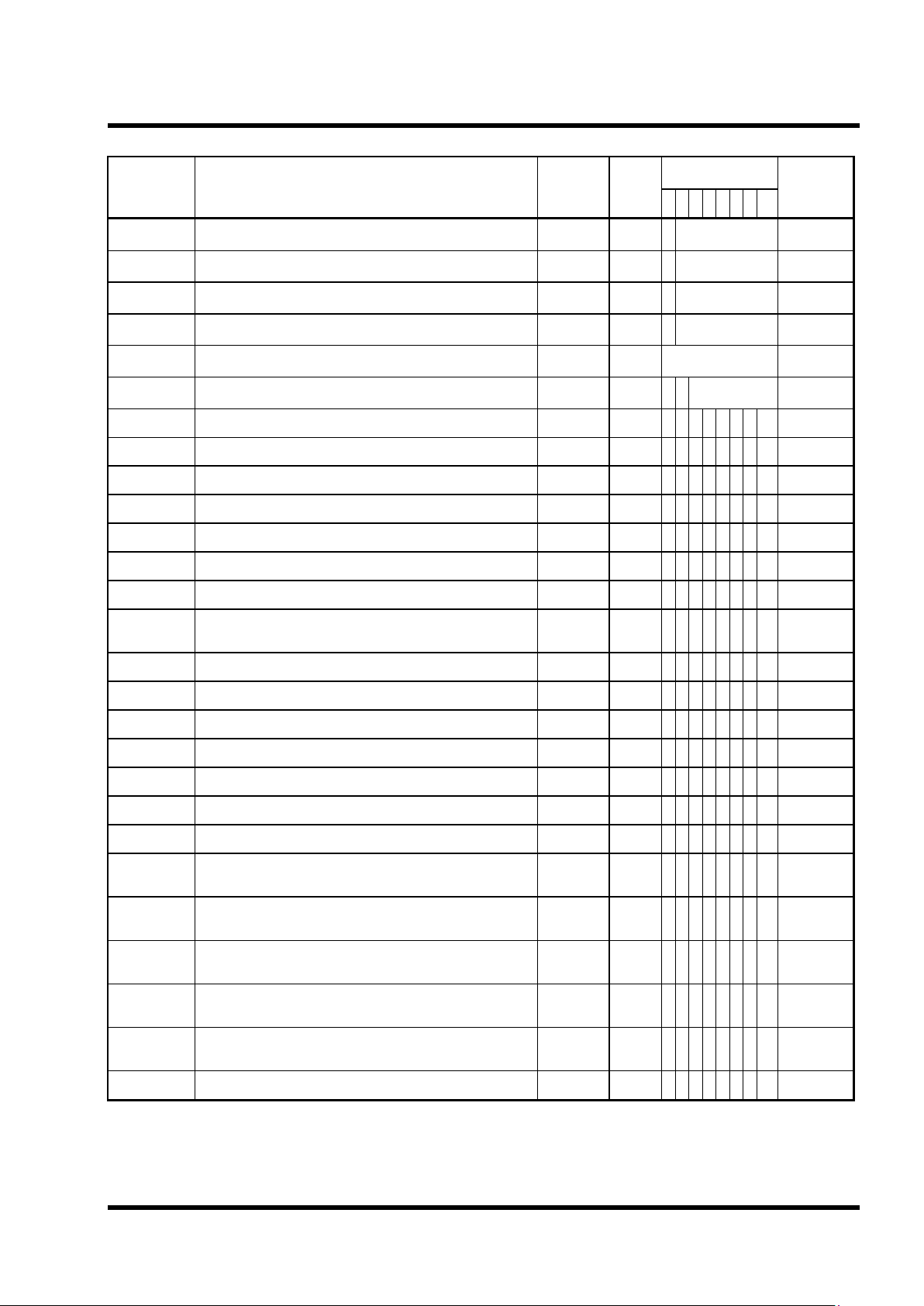
VECTOR AREA
FFC0
H
( L ) FFE0
H
( L )
FFC1
H
( H ) FFE1
H
( H )
FFC2
H
( L ) FFE2
H
( L )
FFC3
H
( H ) FFE3
H
( H )
FFC4
H
( L ) FFE4
H
( L )
FFC5
H
( H ) FFE5
H
( H )
FFC6
H
( L ) FFE6
H
( L )
FFC7
H
( H ) FFE7
H
( H )
FFC8
H
( L ) FFE8
H
( L )
FFC9
H
( H ) FFE9
H
( H )
FFCA
H
( L ) FFEA
H
( L )
FFCB
H
( H ) FFEB
H
( H )
FFCC
H
( L ) FFEC
H
( L )
FFCD
H
( H ) FFED
H
( H )
FFCE
H
( L ) FFEE
H
( L )
FFCF
H
( H ) FFEF
H
( H )
FFD0
H
( L ) FFF0
H
( L )
FFD1
H
( H ) FFF1
H
( H )
FFD2
H
( L ) FFF2
H
( L )
FFD3
H
( H ) FFF3
H
( H )
FFD4
H
( L ) FFF4
H
( L )
FFD5
H
( H ) FFF5
H
( H )
FFD6
H
( L ) FFF6
H
( L )
FFD7
H
( H ) FFF7
H
( H )
FFD8
H
( L ) FFF8
H
( L )
FFD9
H
( H ) FFF9
H
( H )
FFDA
H
( L ) FFFA
H
( L )
FFDB
H
( H ) FFFB
H
( H )
FFDC
H
( L ) FFFC
H
( L )
FFDD
H
( H ) FFFD
H
( H )
FFDE
H
( L ) FFFE
H
( L )
FFDF
H
( H ) FFFF
H
( H )
* This vector area is used in both BRK and TCALL 0 instruction
not used
SERIAL I/O
Basic Interval Timer
Watch Dog Timer
EXT. INT 3
Timer 3
Timer1
V-Sync Interrupt
1mS Interrupt
Timer 2
Timer 0
EXT. INT 2
EXT. INT1
On Screen Display
not used
RESET
TCALL 15
TCALL 14
TCALL 13
TCALL 12
TCALL 11
TCALL 10
TCALL 9
TCALL 8
TCALL 7
TCALL 6
TCALL 5
TCALL 4
TCALL 3
TCALL 2
TCALL 1
TCALL 0 *

GMS84512/84524 USER’ S MANUAL
Table of Contents
1. Overview
2. CPU
3. Peripheral Function
4. Control Function
5. Support Tool
6. Appendix
GMS 84512 / 84524
3- 1
3.1 PORT
There are 6-ports in this device.
You can use these ports an digital I/O or 2nd function I/O
3.1.1 R0 PORT
8-bit I/O port including direction register and port data register (IOA Type)
l Register Structure and Description
Register Name Symbol R/W Address Initial Value
R0 I/O Direction Register R0DD W 00C1
H
0000 0000
R0 PORT Data Register R0 R/W 00C0
H
Not initialized
If output mode port is read, the read data is R0 register data. And if input mode port is read, the
read data is R0 pin data.
Assign the direction of R0 port
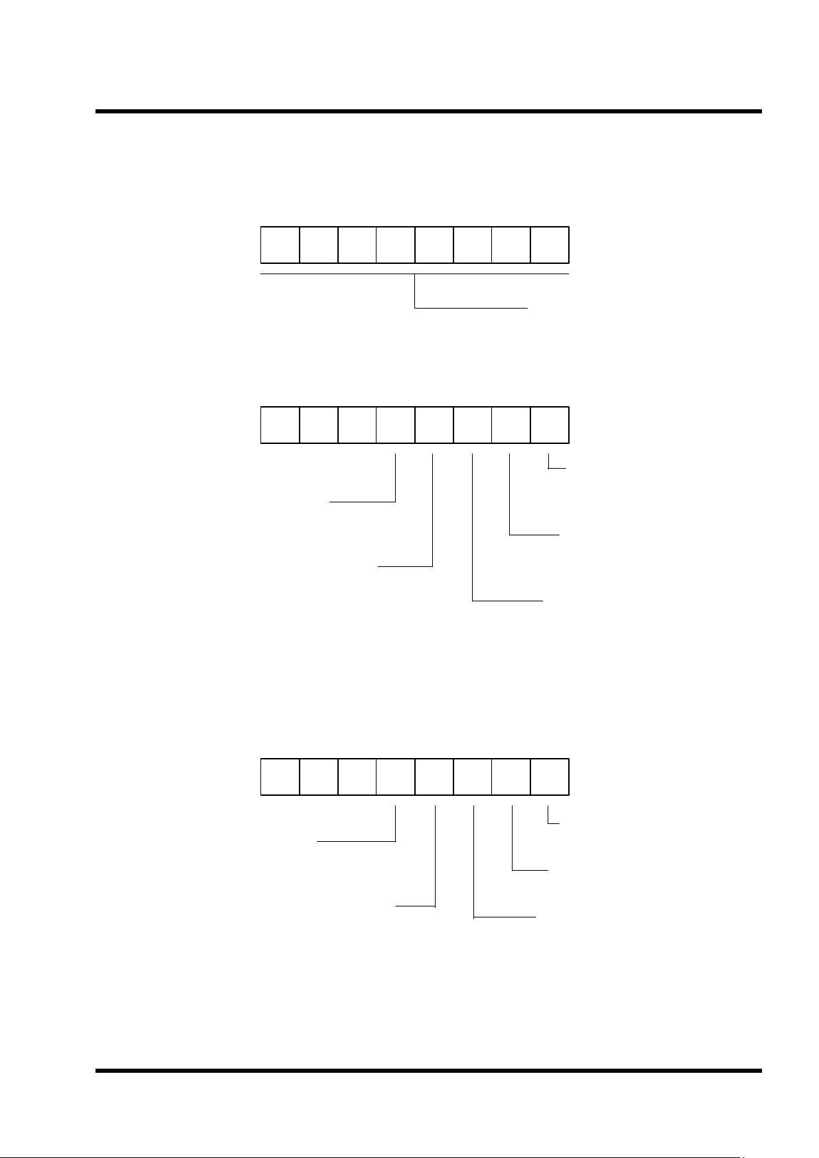
(R0DD0) is assigned to R00 port)
0 : Input
1 : Output
<00C1H>
R0DD
R0 PORT I/O DIRECTION REGISTER
7
R0DD76R0DD65R0DD54R0DD43R0DD32R0DD21R0DD10R0DD0
W W W W W W W W
Initial Value when RESET
[ 0000 0000 ]
Port R0 output data
Initial Value when RESET
[Not initialized ]<00C0H>
R0
R0 PORT DATA REGISTER
7
R076R065R054R043R032R021R010R00
R/W R/W R/W R/W R/W R/W R/W R/W
GMS 84512 / 84524
3 - 2
3.1.2 R1 PORT
You can use the R17 port as input mode only, but others as input or output mode.
Selection Mode
Pin Name Port Selection 2nd Function Type
0 R10 R10 ( I/O ) R10 ( I/O )
IOA
1 R11 R11 ( I/O ) R11 ( I/O )
IOA
2 R12 R12 ( I/O ) R12 ( I/O )
IOA
3 R13 R13 ( I/O ) R13 ( I/O )
IOA
4 R14 R14 ( I/O ) R14 ( I/O )
IOA
5 R15/ Cin1 R15 ( I/O ) Cin1 ( I )
IOC
6 R16/ Cin2 R16 ( I/O ) Cin2 ( I )
IOC
7 R17/ Cin0/ INT3 R17 ( I ) Cin0/ INT3 ( I )
IC
l Register Structure and Description
Register Name Symbol R/W Address Initial Value
R1 I/O Directin Register R1DD W 00C3
H
0000 0000
R1 Port Data Register R1 R/W 00C2
H
Not initialized
A/D COMP. Input CH. Selection Register CIS w 00D7
H
---- --00
Port Function Selection Register FUNC W 00CA
H
---0 0000
R1
PORT
Not used
Assign the direction of R1 port
(R1DD0) is assigned to R10 port)
0 : Input
1 : Output
<00C3H>
R1DD
R1 PORT I/O DIRECTION REGISTER
7
-
6
R1DD65R1DD54R1DD43R1DD32R1DD21R1DD10R1DD0
-
W W W W W W W
Initial Value when Reset
[ -000 0000 ]
GMS 84512 / 84524
3- 3
PORT Selection
CIS1 CIS0 Channel
R15/ Cin1 R16/ Cin2
R17/ Cin0/ INT3R35/ Sin/ Cin3
0 0 Channel 0 (Cin0) R15 R16 Cin0/ INT3 R35/ Sin
0 1 Channel 1 (Cin1) Cin1 R16 R17/ Cin0 R35/ Sin
1 0 Channel 2 (Cin2) R15 Cin2 R17/ Cin0 R35/ Sin
1 1 Channel 3 (Cin3) R15 R16 R17/ Cin0 Cin3
Input data when read Port R1 output data
Initial Value when Reset
[ Not initialized ]<00C2H>
R1
R1 PORT DATA REGISTER
7
-
6
R165R154R143R132R121R110R10
R R/W R/W R/W R/W R/W R/W R/W
R27 / EC3 Selection
0 : R27 ( I/O )
1 : EC3 ( Input )
R17 / INT3 Selection
0 : R17 ( Input )
1 : INT3 ( Input )
R26 / EC2 Selection
0 : R26 ( I/O )
1 : EC2 ( Input )
R31/ INT2 Selection
0 : R31 ( Input )
1 : INT2 ( Input )
R30 / INT1 Selection
0 : R30 ( Input )
1 : INT1 ( Input )
<00CAH>
FUNC
PORT FUNCTION SELECTION REGISTER
7
-
6
-
5
-
4
EC3S3EC2S2INT3S1INT2S0INT1S
- - -
W W W W W
Initial value when MCU Reset
[ ---0 0000 ]
A/D COMP. INPUT CHANNEL SELECTION
Initial Value when Reset
[ ---- --00 ]
<00D7H>
CIS
7
-6-
5
-4-3-
2
-
1
CIS10CIS0
- - - - - -
W W
Analog input channel selection
00 : CIN0
01 : CIN1
10 : CIN2
11 : CIN3
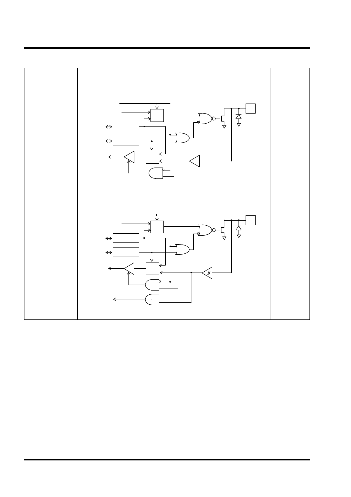
GMS 84512 / 84524
3 - 4
3.1.3 R2 PORT
8- BIT I/O Port
Selection Mode
Pin Name Port Selection 2nd Functin Type
0 R20 R20 ( I/O ) R20 ( I/O )
IOA
1 R21 R21 ( I/O ) R21 ( I/O )
IOA
2 R22 R22 ( I/O ) R22 ( I/O )
IOA
3 R23 R23 ( I/O ) R23 ( I/O )
IOA
4 R24 R24 ( I/O ) R24 ( I/O )
IOA
5 R25/ T2048 R25 ( I/O ) T2048 ( O )
IOD
6 R26/ EC2 R26 ( I/O ) EC2 ( I )
IOB
7 R27/ EC3 R27 ( I/O ) EC3 ( I )
IOB
l Register Structure and Description
Register Name Symbol R/W Address Initial Value
R2 I/O Direction Register R2DD W 00C5
H
0000 0000
R2 Port Data Register R2 R/W 00C4
H
Not initialized
Port Function Selection Register FUNC W 00CA
H
---0 0000
PWM Control Register 2 PWMCR2R/W 00E5
H
---0 0000
R2
PORT
Assign the direction of R2 port
R2DD is assigned to R20 port
0 : Input
1 : Output
<00C5H>
R2DD
R2 PORT I/O DIRECTION REGISTER
7
R2DD76R2DD65R2DD54R2DD43R2DD32R2DD21R2DD10R2DD0
W W W W W W W W
Initial value when MCU Reset
[ 0000 0000 ]
GMS 84512 / 84524
3- 5
Port R2 output data
Initial value when MCU Reset
[ Not initialized ]<00C4H>
R2
R2 PORT DATA REGISTER
7
R276R265R254R243R232R021R210R20
R/W R/W R/W R/W R/W R/W R/W R/W
R27 / EC3 Selection
0 : R27 ( I/O )
1 : EC3 ( Input )
R17 / INT3 Selection
0 : R17 ( Input )
1 : INT3 ( Input )
R26 / EC2 Selection
0 : R26 ( I/O )
1 : EC2 ( Input )
R31/ INT2 Selection
0 : R31 ( Input )
1 : INT2 ( Input )
R30 / INT1 Selection
0 : R30 ( Input )
1 : INT1 ( Input )
<00CAH>
FUNC
PORT FUNCTION SELECTION REGISTER
7
-
6
-
5
-
4
EC3S3EC2S2INT3S1INT2S0INT1S
- - -
W W W W W
Initial value when MCU Reset )
[ ---0 0000 ]
PWM OUTPUT CONTROL REGISTER 2
Initial value when MCU Reset
[ ---0 0000 ]
<00E5H>
PWMCR2
7
-
6
-
5
-
4
T20483POL22POL11EN70EN6
- - -
R/W R/W R/W R/W R/W
R25/ T2048 Selection
0 : R25
1 :T2048 (Output rectangular wave(T=2048uS)
7-bit PWM OUTPUT Polarity
0 : Positive Polarity
1 : Negative Polarity
14-bit PWM Output Polarity
0 : Positive poarity
1 : Negative Polarity
R36/ PWM7 Selection
0 : R36
1 : PWM7
R37/ PWM6 Selection
0 : R37
1 : PWM6
 Loading...