


8-BIT SINGLE-CHIP MICROCONTROLLERS
GMS87C4060
GMS81C4040
User’s Manual
MicroElectronics
Semiconductor Group of Hyundai Electronics Industrial Co., Ltd.

Additional information of this manual may be served by HYUNDAI Micro Electronics offices in Korea or Distributors and Representatives listed at address directory.
HYUNDAI Micro Electronics res erves the right to make changes to any information here in at any time without
notice.
The information, diagrams and other data in this manual are correct and reliable; however, HYUNDAI Micro
Electronics is in no way responsible for any violations of patents or other rights of the third party generated by
the use of this manual.
Versi on 1.00
Published by
MCU Application Team bjli m@hmec.co.kr conner@hmec.co. kr
2000 HYUNDAI Micro Electronics All right reserved.

PRELIMINARY
GMS81C4040/87C4060
Nov. 1999 Ver 1.0
PRELIMINARY
1
Table of Contents
OVERVIEW.......................................... 1
Description...................................................1
Features .......................................................1
Development Tools..................................... 2
BLOCK DIAGRAM.............................. 3
PIN ASSIGNMENT.............................. 4
PACKAGE DIAGRAM .........................5
PIN FUNCTION ....................................6
PORT STRUCTURES ..........................9
RESET................................................................ 9
TEST................................................................... 9
XIN, XOUT ........................................................9
OSC1, OSC2 ..................................................... 9
R00~07, R53 ...................................................... 9
R10~15 (AN0~5) ................................................ 9
R16, 17, 20, 24, 25, 26, 27, 52, 67 ................... 10
R21/Sclk, R22/Sout .......................................... 10
R23/Sin ............................................................ 10
R40~43 (PWM0~3) .......................................... 10
R44, 45, 46, 47 (SCL, SDA, PWM) ..................10
R50/BUZZ, R51/PWM8 ........ ......... ................. ..11
R54/YM, R55/YS, R56/I ...................................11
R, G, B ............................................................. 11
ELECTRICAL CHARACTERISTICS . 12
Absolute Maximum Ratings .....................12
Recommended Operating Conditions ....12
DC Electr i cal Characteristics - GM S81C404 0
.....................................................................12
A/D Comparator Characteristics .............14
AC Characteristics ....................................14
Typical Characteristics ............................16
MEMORY ORGANIZATION .............. 17
Registers ...................................................17
Program Memory ........ ............... .............. .20
PCALL→ rel ..................................................... 21
TCALL→ n ....................................................... 21
Data Memory ........ ............... .............. ........23
User Memory .................................................... 23
Control Registe rs ........................................... ..23
Stack Area ........................................................23
Addressing Mode ......................................25
(1) Register Addressing ...................................25
(2) Immediate Addressing → #imm .................. 25
(3) Direct Page Addressing → dp ....... .............. 25
(4) Absolute Addressing → !abs ....................... 25
(5) Indexed Addressing .................................... 26
X indexed direct page (no offset) → {X} ...........26
X indexed direct page, auto increment→ {X}+ . 26
X indexed direct page (8 bit offset) → dp+X .....26
Y indexed direct page (8 bit offset) → dp+Y .....27
Y indexed absolute → !abs+Y ..........................27
Direct page indirect → [dp] ...............................27
X indexed indirect → [dp+X] ............................. 27
Y indexed indirect → [dp]+Y ............................. 28
Absolute indirect → [!abs] ................................28
I/O PORTS ......................................... 29
Registers for Port .............. .............. .........29
Port Data Registers ..........................................29
I/O Ports Configuration ............................3 0
R0 Ports ...........................................................30
R1 Ports ...........................................................30
R2 Port .............................................................31
R4 Port .............................................................31
R5 Port .............................................................32
R6 Port .............................................................32
CLOCK GENERATOR ...................... 33
TIMER ................................................ 34
Basic Interval Timer .................................34
Timer 0, 1 ................. .............. ............... .....35
Timer / Event Counter 2, 3 ....... ............... .37
Timer Mode ...................................................... 39
Event counter Mode ......................................... 39
A/D Converter ................................... 42
Control ..............................................................42
Serial I/O ........................................... 44
Control ..............................................................44
Pulse Width Modulation (PWM) ...... 46
8bit PWM Control ............................................. 47
14bit PWM Control ........................................... 47
Interrupt interval measurement circuit
........................................................... 49
Control ..............................................................49
Buzzer driver .................................... 51
Control ..............................................................51
On Screen Display (OSD) ................ 53
OSDCON1 ....................................................... 55
OSDCON2 ....................................................... 55
OSDPOL .......................................................... 56
FDWSET .......................................................... 56
L1ATTR ............................................................ 57
L1VPOS ........................................................... 58
L2ATTR ............................................................ 58
L2VPOS ........................................................... 58
COLMOD ......................................................... 58
MESHCON ....................................................... 58
VRAM ...............................................................58
Font ROM .........................................................60

GMS81C4040/87C4060
PRELIMINARY
2
PRELIMINARY
Nov. 1999 Ver 1.0
Sprite RAM ....................................................... 60
Test Font ..........................................................61
I2C Bus Interface ..............................62
Control .......... ................. ................ ................. ..62
I2C address register ......................................... 62
I2C data shift register [ICDR] ........................... 63
I2C status register ............................................63
I2C control register 1 ........................................ 64
I2C control register 2 ........................................ 64
START condition generation ............................ 65
RESTART condition generation ....................... 65
STOP condition generation .............................. 65
START / STOP condition detect ...................... 66
Address data communication ........................... 67
INTERRUPTS .................................... 68
Interrupt Mode Register ...................................68
Interrupt Sequence ......... .............. ............72
Interrupt acceptance ........................................72
Saving/Restoring General-purpose Register ... 73
Multi Interrupt ............................................74
External Interrupt .............. .............. .........75
Response Time ........... .......... ................ ........... 75
WATCHDOG TIMER ......................... 76
Watchdog Timer Control ..................................76
Enable and Disable Watchdog .........................77
Watchdog Timer Interrupt ................................77
Minimizing Current Consumption ..................... 78
OSCILLATOR CIRCUIT .................... 80
RESET ............................................... 81
External Reset Input ................. ............... .81
Watchdog Timer Reset ............................82
OTP Programming ........................... 83
GMS87C4060 OTP Programming ............83
.Device configuration data ......................84
Timing Chart .............................................87
Assemble mnemonics ..................... 89
Instruction Map ............................. ............89
Alphabetic order table of instruction .....90
Instruction Table by Function .................94
PRELIMINARY
GMS81C4040/87C4060
Nov. 1999 Ver 1.0
PRELIMINARY
1
GMS81C4040/GMS87C4060
CMOS SINGLE-CHIP 8-BIT MICROCONTROLLER
FOR TELEVI SI ON
1. OVERVIEW
1.1 Description
The GMS81C4040/GMS87C4 060 is an adva nced CMOS 8-bi t micro control le r with 40K( 60K) bytes of ROM. T he device i s
one of GMS800 family. The HYUNDAI’s GMS81C4040/GMS87C4060 is a powerful microcontroller which provides a
highly flexible and cost effectiv e solution to many TV applications. The GMS81C4040/GMS87C4060 provides t he following standard features: 40K(60K) bytes of ROM, 1,536 bytes of RAM, 8-bit timer/counter .
1.2 Features
• 40K(60K) Bytes On-chip Program Memory
• 1,536 Bytes of On-chip Data RAM
(Included 256 bytes stack memory)
• Instruction Cycle Time (ex:NOP)
- 0.5us at 8MHz
• 40 Program m able I/O pins
- 33 I/O and 7 Outp ut pi ns
• Serial I/O : 8bit x 1ch
•I
2
C Bus interface
- Multimaster (2 Pairs interface pins)
• A/D Converter : 8bit x 6ch (TBD LSB)
• Pulse Width Modulation
- 14bit x 1ch
- 8bit x 6ch
•Timer
- Timer/Counter : 8bit x 4ch (16bit x 2ch)
- Basic interval timer : 8bit x 1ch
- Watch Dog Timer
• Number of Interrupt sources : 18
• On Screen Display
- Number of characters : 512 (6 characters are
reserved for IC test)
- Character size : 12 dots(X) x 16 dots(Y)
- Character display size : Large, Medium, Small
- DIsplay capability : 24Characters x 16 Line
(Two line VRAM buffer)
- Character, Back ground color : 16kinds
- Special functions : Rounding, Outline, Sprite,
Shadow,...
• Buzz er D riv in g port
- 500Hz ~ 250kHz @8MHz (Duty 50%)
• Operating Range : 4.5V to 5.5V
Device name ROM Size RAM Size Package
GMS81C4040
40K bytes
Mask ROM
1,536 bytes 52SDIP
GMS87C4060
60K bytes
EPROM
1,536 bytes 52SDIP

GMS81C4040/87C4060
PRELIMINARY
2
PRELIMINARY
Nov. 1999 Ver 1.0
1.3 Development Tools
The GMS81C4040/GMS87C4060 is supported by a fullfeatured macro as sem bler / linker , OSD font editor, an incircuit emulator CHOICE-Dr
TM
.
In Circuit Emulators
CHOICE-Dr.
(with EVA81C4xxx board)
Assembler / Linker
HYUNDAI’s Macro Assembler /
Linker
Font Editor
MS-Windows GUI version
Debugger
MS-Windows GUI version
PRELIMINARY
GMS81C4040/87C4060
Nov. 1999 Ver 1.0
PRELIMINARY
3
2. BLOCK DIAGRAM
ALU
OSD (On Screen Display) Controller
Accumulator
Interrupt Controller
Data
Memory
OSD
Memory
Display
8-bit x 4
Counter
Timer/
Program
Memory
Vector Table
8-bit Basic
Timer
Interval
Watchdog
Timer
PSW
System controller
Timing generator
System
Clock Controller
RESET
TEST
XIN
XOUT
OSC1
OSC2
R,G,B
VDD
VSS
Power
Supply
R1
Clock generator
& Index X,Y
8bit A/D
Convertor
Buzze r
R5
PWM
14bit x 1
8bit x 6
Da ta b u s
I2C
Interf a c e
R4
Da ta b u s
Serial I/O
Inte rfac e
Interrupt
Interv a l
Measure
R2
R0 R6
Stack pointer
PC
R00
R01
R02
R03
R04
R05
R06
R07
R67 / INT1
R20 / INT2
R21 / Sclk
R22 / Sout
R23 / Sin
R24 / INT3
R25 / EC2
R26 / INT4
R27 / EC3
R40 / PWM0
R41 / PWM1
R42 / PWM2
R43 / PWM3
R44 / SCL0
R45 / SCL1 / PWM4
R46 / SDA0
R47 / SDA1 / PWM5
R10 / AN0
R11 / AN1
R12 / AN2
R13 / AN3
R14 / AN4
R15 / AN5
R16 / VD
R17 / HD
R50 / BUZZ
R51 / PWM8
R52 / INT0
R53
R54 / YM
R55 / YS
R56 / I
GMS81C4040/87C4060
PRELIMINARY
4
PRELIMINARY
Nov. 1999 Ver 1.0
3. PIN ASSIGNMENT
R40/PWM0
R41/PWM1
R42/PWM2
R43/PWM3
R44/SCL0
R45/SCL1/PWM4
R46/SDA0
R47/SDA1/PWM5
R50/BUZZ
R51/PWM8
R52/INT0
R53
Vss
Vdd
TEST
OSC1
OSC2
R54/YM
R55/YS
R56/I
B
G
R
R00
R01
R02
R27/EC3
R26/INT4
R25/EC2
R24/INT3
R23/Sin
R22/Sout
R21/Sclk
R20/INT2
R17/HD
R16/VD
RESET
Vss
Xout
Xin
R15/AN5
R14/AN4
R13/AN3
R12/AN2
R11/AN1
R10/AN0
R07
R06
R05
R04
R03
R67/INT1
52
51
50
49
48
47
46
45
44
43
42
41
40
39
38
37
36
35
34
33
32
31
30
29
28
27
1
2
3
4
5
6
7
8
9
10
11
12
13
14
15
16
17
18
19
20
21
22
23
24
25
26
HYUNDAI
GMS81C40XX
PRELIMINARY
GMS81C4040/87C4060
Nov. 1999 Ver 1.0
PRELIMINARY
5
4. PACKAGE DIAGRAM
Figure 4-1 52pin Shrink DIP Package Diagram
UNIT: mm
HYUNDAI
GMS81C40XX
1
26
2752
45.97
0.13
0.76
0.13
1.778
0.25
4.38 Max.
13.97
0.25
15.24
0.25
0.47 0.13 1.02 0.25
3.81 0.13
3.24
0.20
0.50 Min.
0.25 0.05
0 ~ 15

GMS81C4040/87C4060
PRELIMINARY
6
PRELIMINARY
Nov. 1999 Ver 1.0
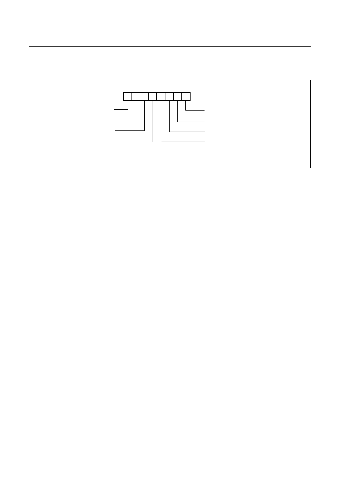
5. PIN FUNCTION
V
DD
: Supply voltage.
V
SS
: Circuit ground.
TEST
: Used for shipping inspection of the IC. For normal
operation, it should not be connected .
RESET
: Rese t th e MCU.
X
IN
: Input to the inver tin g oscil lator ampli fie r and i nput to
the internal main clock operating circuit.
X
OUT
: Output from the inverting oscillator amplifier.
OSC1
: Input to the internal On Screen Display operating
circuit.
OSC2
: Output from the inverting OSC1 amplifier.
R00~R07
: R0 is an 8-bit CMOS bidi rec tional I/O port. R0
pins 1 or 0 written to the Port Direction Register can be
used as outputs or inpu ts.
R10~R17
: R1 is an 8-bit CMOS bidi rec tional I/O port. R1
pins 1 or 0 written to the Port Direction Register can be
used as outputs or inpu ts.
In addition, R1 serves the functions of the various following special features.
R20~R27
: R2 is a 8-bit CMOS bidi rectional I/O por t. Each
pins 1 or 0 written to the their Port Direction Register can
be used as outputs or inputs.
In addition, R2 serves the functions of the various following special features.
R40~R47
: R40~R43 are 8-bit NM OS open drain output
and R45~R47 are bidirec tional CMOS Input / NMOS open
drain output port. R4 pins 1 or 0 written to the Port Direction Registe r can be used as outputs or inputs .
In addition, R4 serves the functions of the various following sp ec ial featu r es.
R50~R56
: R50~R53 are 4-bi t CMOS bidire ctional I/ O and
R54~R56 are CMOS output port. R5 p ins 1 or 0 written to
the Port Direction Register can be used as outputs or inputs.
In addition, R5 serves the functions of the various following sp ec ial featu r es.
R67
: R67 is an 1- bit CMOS bidirection al I/O port. R67
pins 1 or 0 written to the Port Direction Register can be
used as outputs or inputs.
In addition, R67 serves the functions of the vario us following sp ec ial featu r es.
R,G,B
: R,G,B CMOS outpu t port. E ach pin s cont rols Re d,
Green,. Blue color co ntrol.
Port pin Alternate funct ion
R10
R11
R12
R13
R14
R15
R16
R17
AN0 (A/D converter input 0)
AN1 (A/D converter input 1)
AN2 (A/D converter input 2)
AN3 (A/D converter input 3)
AN4 (A/D converter input 4)
AN5 (A/D converter input 5)
VD (Vertical Sync. input)
HD (Horisontal Sync. input)
Port pin Alternate funct ion
R20
R21
R22
R23
R24
R25
R26
R27
INT2 (External interrupt input 2)
Sclk (Serial communication clock)
Sout (Serial communication data out)
Sin (Serial communi cation data in)
INT3 (External interrupt input 3)
EC2 (Event counter in put 2)
INT4 (External interrupt input 4)
EC3 (Event counter in put 3)
Port pin Alternate function
R40
R41
R42
R43
R44
R45
R46
R47
PWM0 (Pulse Width Modul ation output 0)
PWM1 (Pulse Width Modul ation output 1)
PWM2 (Pulse Width Modul ation output 2)
PWM3 (Pulse Width Modul ation output 3)
SCL0 (I
2
C Clock 0)
SCL1 (I
2
C Clock 1)
PWM4 (Pulse Width Modul ation output 4)
SDA0 (I
2
C Data 0)
SDA1 (I
2
C Data 1)
PWM5 (Pulse Width Modul ation output 5)
Port pin Alternate function
R50
R51
R52
R54
R55
R56
BUZZ (Buzzer output)
PWM8 (Pulse Width Modul ation output 8)
INT0 (External int errupt input 0)
YM (Back ground)
YS (Edge)
I (Intencity)
Port pin Alternate function
R67 INT1 (External int errupt input 1)
PRELIMINARY
GMS81C4040/87C4060
Nov. 1999 Ver 1.0
PRELIMINARY
7
PIN NAME Pin No. In/Out Function
V
DD
39 - Supply voltage
V
SS
12, 40 - Circuit ground
TEST
38 I For test purposes. Should not be connected. (N.C.)
RESET
11 I Reset signal input
X
IN
14 I Main oscillation input
X
OUT
13 O Main oscillation output
OSC1 37 I
On screen display functions
On screen display oscillation input
OSC2 36 O On screen display osc. output
R17/HD 9 I/O Horisontal Sync. input
R16/VD 10 I/O Vertical Sync. input
R 30 O Red signal output
G 31 O Green signal output
B 32 O Blue signal output
R56/I 33 O Intencity sign al output
R55/YS 34 O Edge signal output
R54/YM 35 O Background signal output
R40/PWM0 52 O
PWM functions
8bit PWM
R41/PWM1 51 O 8bit PWM
R42/PWM2 50 O 8bit PWM
R43/PWM3 49 O 8bit PWM
R45/SCL1/
PWM4
47 I/O
Include I
2
C Serial clock 1 (SCL1)
R47/SDA1/
PWM5
45 I/O
Include I
2
C Serial data 1 (SDA1)
R51/PWM8 43 I/O 14bit PWM
R44/SCL0 48 I/O
I
2
C functions
I
2
C Serial clock 0
R46/SDA0 46 I/O
I
2
C Serial data 0
R23/Sin 5 I/O
SCI functions
Serial data input
R22/Sout 6 I/ O Ser ial data output
R21/Sclk 7 I/O Serial communication clock
R27/EC3 1 I/O
Timer event functions
Event counter input 3
R25/EC2 3 I/O Event counter input 2
R50/Buzzer 44 I /O Buzzer function 500Hz ~ 250KHz @8MHz
Table 5-1 Port Function Description
GMS81C4040/87C4060
PRELIMINARY
8
PRELIMINARY
Nov. 1999 Ver 1.0
R52/INT0 42 I/O
External interrupt functions
External interrupt input 0
R67/INT1 26 I/O External interrupt input 1
R20/INT2 8 I/O External interrupt input 2
R24/INT3 4 I/O External interrupt input 3
R26/INT4 2 I/O External interrupt input 4
R10/AN0 20 I/O
A/D conversion functions
Analog input 0
R11/AN1 19 I/O Analog input 1
R12/AN2 18 I/O Analog input 2
R13/AN3 17 I/O Analog input 3
R14/AN4 16 I/O Analog input 4
R15/AN5 15 I/O Analog input 5
R00 29 I/O
Digital I/O functions
R01 28 I/O
R02 27 I/O
R03 25 I/O
R04 24 I/O
R05 23 I/O
R06 22 I/O
R07 21 I/O
R53 41 I/O
PIN NAME Pin No. In/Out Function
Table 5-1 Port Function Description
PRELIMINARY
GMS81C4040/87C4060
Nov. 1999 Ver 1.0
PRELIMINARY
9
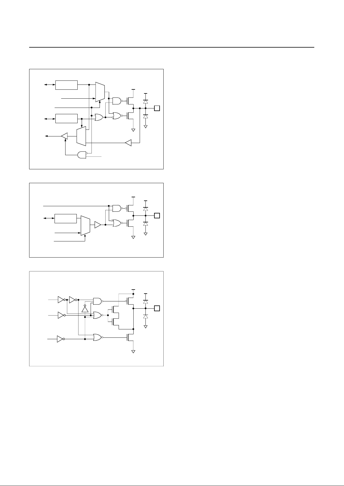
6. PORT STRUCTURES
RESET
TEST
XIN, X
OUT
OSC1, OSC2
R00~07, R53
R10~15 (AN0~5)
RESET
V
DD
V
SS
Noise
Canceler
V
DD
V
SS
X
IN
X
OUT
V
SS
V
DD
V
SS
V
DD
Main frequency
clock
V
SS
OSDON
OSC1
OSC2
V
SS
V
DD
V
SS
V
DD
Main frequency
clock
Pin
Data Reg.
Dir. Reg.
DB
DB
DB
MUX
RD
V
DD
V
SS
Pin
Data Reg.
Dir. Reg.
DB
DB
DB
MUX
RD
V
DD
V
SS
AN0~5
GMS81C4040/87C4060
PRELIMINARY
10
PRELIMINARY
Nov. 1999 Ver 1.0
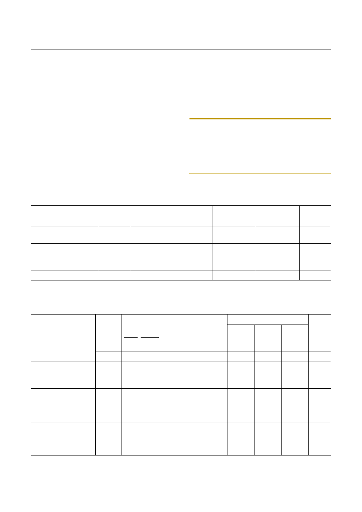
R16, 17, 20, 24, 25, 26, 27, 52, 67
R21/Sclk, R22/So ut
R23/Sin
R40~43 (PWM0~3)
R44, 45, 46, 47 (SCL, SDA, PWM)
Pin
Data Reg.
Dir. Reg.
DB
DB
DB
MUX
RD
V
DD
V
SS
HD,VD,
EC2~3
INT0~INT4
Pin
Data Reg.
Dir. Reg.
DB
DB
DB
MUX
RD
V
DD
V
SS
Sclk
MUX
Sout, Sclk
Selection
Pin
Data Reg.
Dir. Reg.
DB
DB
DB
MUX
RD
V
DD
V
SS
Sin
Selection
Pin
Data Reg.
DB
V
SS
MUX
PWM0~3
Selection
Pin
Data Reg.
Dir. Reg.
DB
DB
DB
MUX
RD
V
SS
SCL, SDA
MUX
PWM4,PWM5
Selection
SCL,SDA
PRELIMINARY
GMS81C4040/87C4060
Nov. 1999 Ver 1.0
PRELIMINARY
11
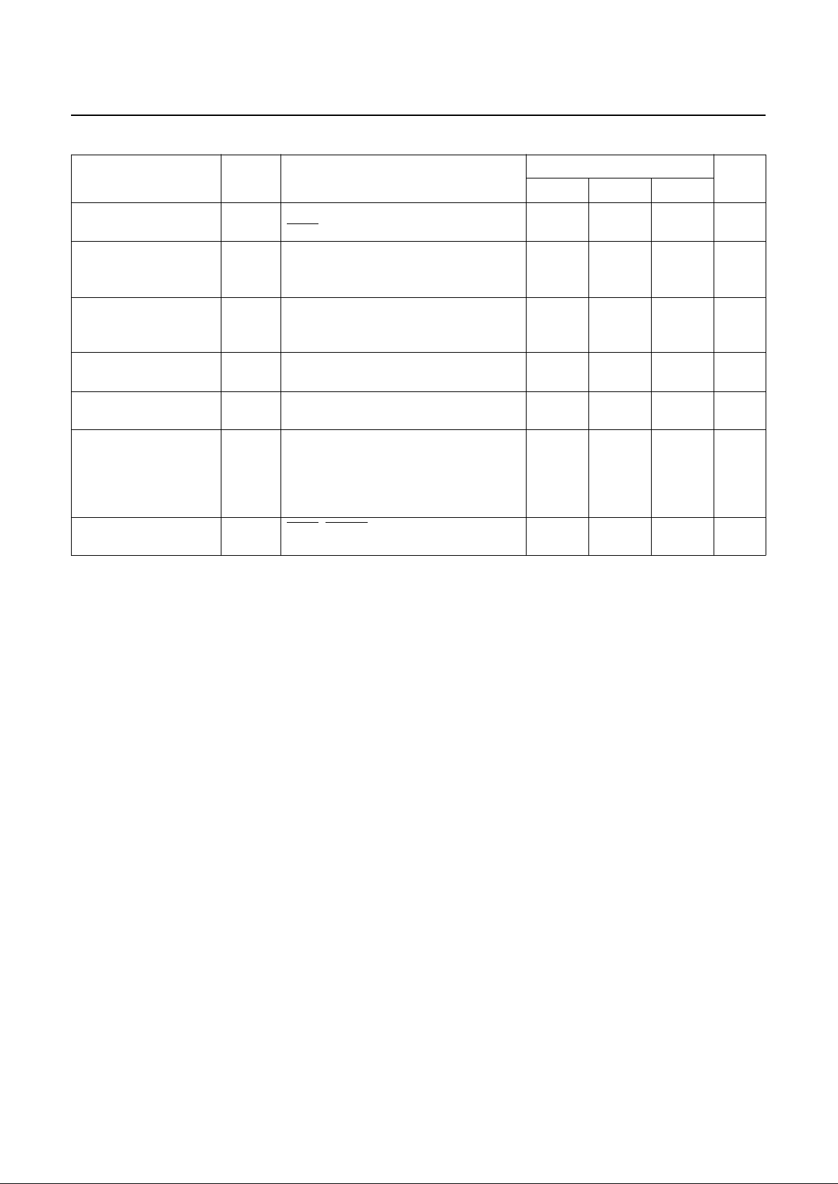
R50/BUZZ, R51/PWM8
R54/YM, R55/YS, R56/I
R, G, B
Pin
Data Reg.
Dir. Reg.
DB
DB
DB
MUX
RD
V
DD
V
SS
MUX
Buzz, PWM8
Selection
Pin
Data Reg.
DB
V
DD
V
SS
MUX
YM, YS, I
Selection
OSD ON or Data Reg Write.
Pin
R, G, B
V
DD
V
SS
i
OSD_ON
GMS81C4040/87C4060
PRELIMINARY
12
PRELIMINARY
Nov. 1999 Ver 1.0
7. ELECTRICAL CHARACTERISTICS
7.1 Absolute Maximum Ratings
Supply voltage...........................................-0.3 to +6.0 V
Storage Temperature ................................-40 to +125 °C
Voltage on any pin with respect to Ground (V
SS
)
............................................................... -0.3 to V
DD
+0.3
Maximum current out of V
SS
pin ........................100 mA
Maximum current into V
DD
pin ............................80 mA
Maximum current sunk by (I
OL
per I/O Pin) ........20 mA
Maximum output current sourced by (I
OH
per I/O Pin)
...... .. .. .......................................................................8 mA
Maximum current (ΣI
OL
)......................................80 mA
Maximum current (ΣI
OH
)......................................50 mA
Note:
Stresses above those listed under "Absolute Maximum Ratings" may cause pe rmanent dam age to the device. This is a stress rating only and functional operation of
the device at a ny other conditio ns above those ind icated in
the operational sections of this specification is not implied.
Exposure to abso lute maximum rati ng conditions for extended periods may aff ect device reliability.
7.2 Recommended Operating Conditions
7.3 DC El ectrical Ch ar acteristi cs - GMS81C4040
(TA=-10~70°C, VDD=4.5~5.5V)
,
Parameter Symbol Condition
Specifications
Unit
Min. Max.
Supply Voltage
V
DD
f
XIN
=8MHz
f
OSC
=16MHz
4.5 5.5 V
Operating Frequency
f
XIN
VDD=4.5~5.5V
48MHz
On Screen Display Operating Frequency
f
OSC
VDD=4.5~5.5V
816MHz
Operating Temperature
T
OPR
-10 70
°
C
Parameter Symbol Condition
Specifications
Unit
Min. Typ. Max.
High level input vol tage
V
IH1
TEST, RESET, Xin, OSC1, R17~16,
R27~20, R47~44, R52, R67
0.8 V
DD
-
V
DD
V
V
IH2
R0, R15~10, R53~50
0.7 V
DD
-
V
DD
V
Low leve l in put vo lta g e
V
IL1
TEST, RESET, Xin, OSC1, R17~16,
R27~20, R47~44, R52, R67
0-
0.12 V
DD
V
V
IL2
R0, R15~10, R53~50 0 -
0.3 V
DD
V
High level output voltage
V
OH
I
OH
= -5mA
R0, R1, R2, R5, R67
V
DD
- 1
--V
I
OH
= -1.2mA
R,G,B
V
DD
- 1
--V
Low level output voltage
V
OL
I
OL
= 5mA
R0, R1, R2, R4, R5, R67, R, G, B
-
-1.0V
Supply current in
ACTIVE mode
I
DD
V
DD
--30mA
PRELIMINARY
GMS81C4040/87C4060
Nov. 1999 Ver 1.0
PRELIMINARY
13
pull-up lekage current
I
RUP
VDD = 5.5v, V
PIN
= 0.4V
TEST
-1.5 -400
µ
A
High input leakage
current
I
IZH
V
DD
= 5.5V, V
PIN
= V
DD
All input, I/O pin s except XIN, OSC1,
R47~40
-5 - 5
µ
A
Low input leakage
current
I
IZL
V
DD
= 5.5V, V
PIN
= 0V
All input, I/O pin s except X
IN
, OSC1,
R47~44
-5 - 5
µ
A
Open drain leakage
current
I
LOZ
V
DD
= 5.5V, V
OH
= VDD, N-ch Tr. off
R47~40
--10µA
RAM data retention
voltage
V
RAMVDD
1.2 - - V
I
2
C port impedance
(I/O Tra n s is to r o ff)
R
BS
V
DD
= 4.5V
,
V
SCL0
= V
SCL1
= 2.25V
V
SDA0
= V
SDA1
= 2.25V
SCL0:SCl1 (R44:R45)
SDA0:SDA1 (R46:R47)
- - 120
Ω
Hysterisis
Vt+ ~
Vt-
TEST
, RESET, Xin, OSC1, R17~16,
R27~20, R47~44, R52, R67
1.0 - - V
Parameter Symbol Condition
Specifications
Unit
Min. Typ. Max.
GMS81C4040/87C4060
PRELIMINARY
14
PRELIMINARY
Nov. 1999 Ver 1.0
7.4 A/D Comparator Characteristics
(TA=-10~70°C, VDD=5.0V)
7.5 AC Characteristics
(TA=-10~70°C, VDD=5V±10%, VSS=0V)
Parameter Symbol Pins
Specifications
Unit
Min. Typ. Max.
Analog Input Voltage Range
V
AIN
AN0~AN5
V
SS
-
V
DD
V
Accuracy
N
FS
---
ΤΒ∆
LSB
Parameter Symbol Pins
Specifications
Unit
Min. Typ. Max.
Operating Frequency
f
XIN
X
IN
4-8MHz
f
OSC
OSC 8 - 16 MHz
External Clock Pulse Width
t
MCPW
X
IN
62.5 - 125 nS
t
SCPW
S
CLK
0.5 -
µ
S
External Clock Transition Time
t
MRCP,tMFCP
X
IN
- - 20 nS
t
SRCP,tSFCP
S
CLK
- - 20 nS
Oscillation Stabilizing Time
t
ST
XIN, X
OUT
--20mS
Interrupt Pulse Width
t
IW
INT0~4 2 - -
t
SYS
1
RESET Inpu t Width
t
RST
RESET 8--
t
SYS
1
Event Counter Input Pulse
Width
t
ECW
EC2, EC3 2 - -
t
SYS
1
Event Counter Transition Time
t
REC,tFEC
EC2, EC3 - - 20 nS
1. t
SYS
is one of 2/f
XIN
main cloc k operation mode,
PRELIMINARY
GMS81C4040/87C4060
Nov. 1999 Ver 1.0
PRELIMINARY
15
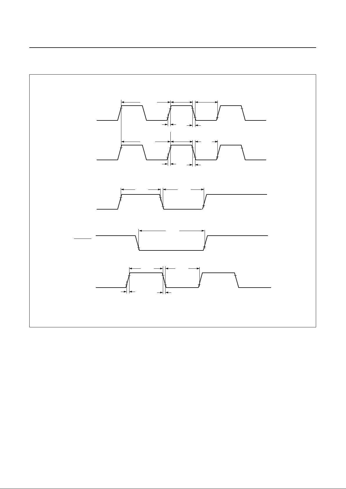
Figure 7-1 Timing Chart
t
MRCP
t
MFCP
X
IN
INT0 ~ 4
0.5V
V
DD
-0.5V
0.2V
DD
0.8V
DD
0.2V
DD
RESET
t
REC
t
FEC
0.2V
DD
0.8V
DD
EC2, EC3
t
IW
t
IW
t
RST
t
ECW
t
ECW
1/f
XIN
t
MCPW
t
MCPW
t
SRCP
t
SFCP
S
CLK
0.5V
V
DD
-0.5V
1/f
SCLK
t
SCPW
t
SCPW

GMS81C4040/87C4060
PRELIMINARY
16
PRELIMINARY
Nov. 1999 Ver 1.0
7.6 Typical Characteristics
This data will generate after evaluation.
Not available at this time.
PRELIMINARY
GMS81C4040/87C4060
Nov. 1999 Ver 1.0
PRELIMINARY
17
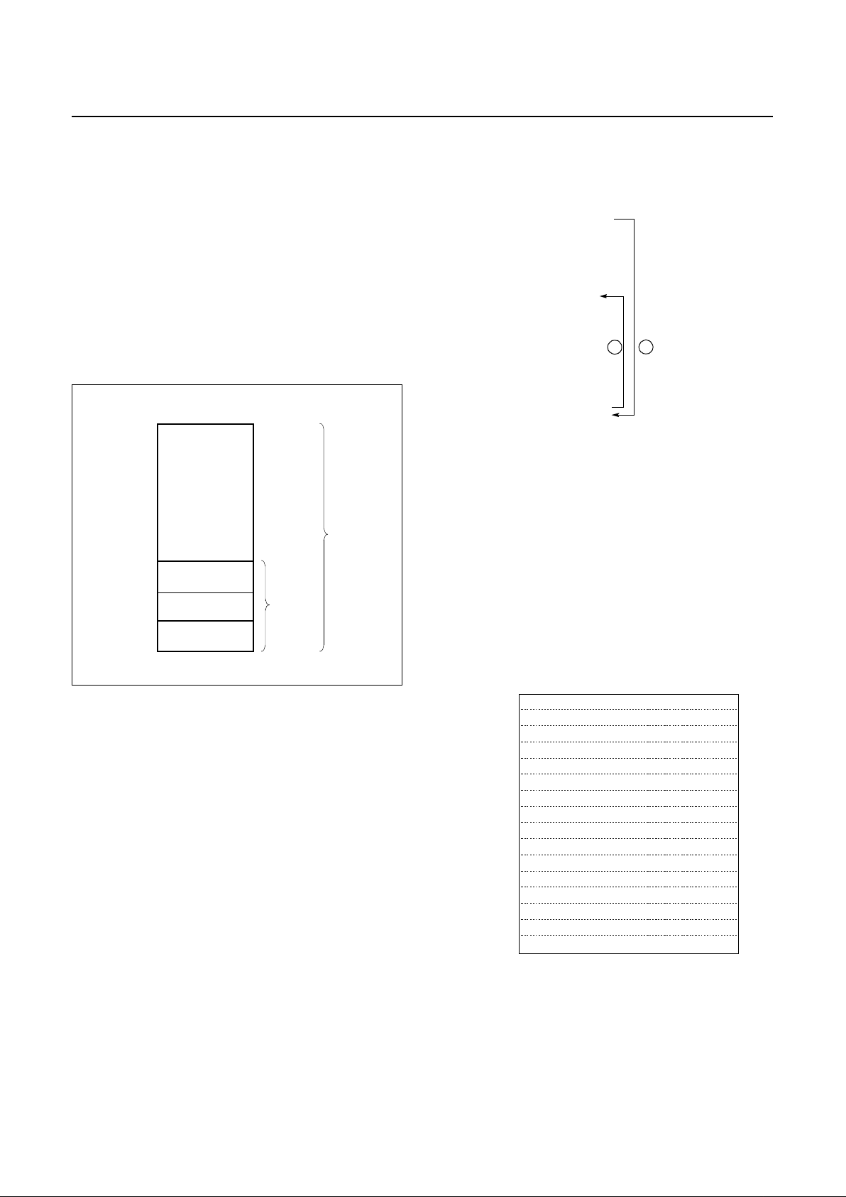
8. MEMORY ORGANIZATION
The GMS81C4040/GMS87C4060 has separate address
spaces for P rogram memo ry, Data M emory and D isplay
memory. Program memory can only be read, not written
to. It can be up to 40K/60K byte s of Program memo ry.
Data memory can be read and written to up to 1,536 bytes
including the stack area. Font memory has prepared 16K
bytes for OSD.
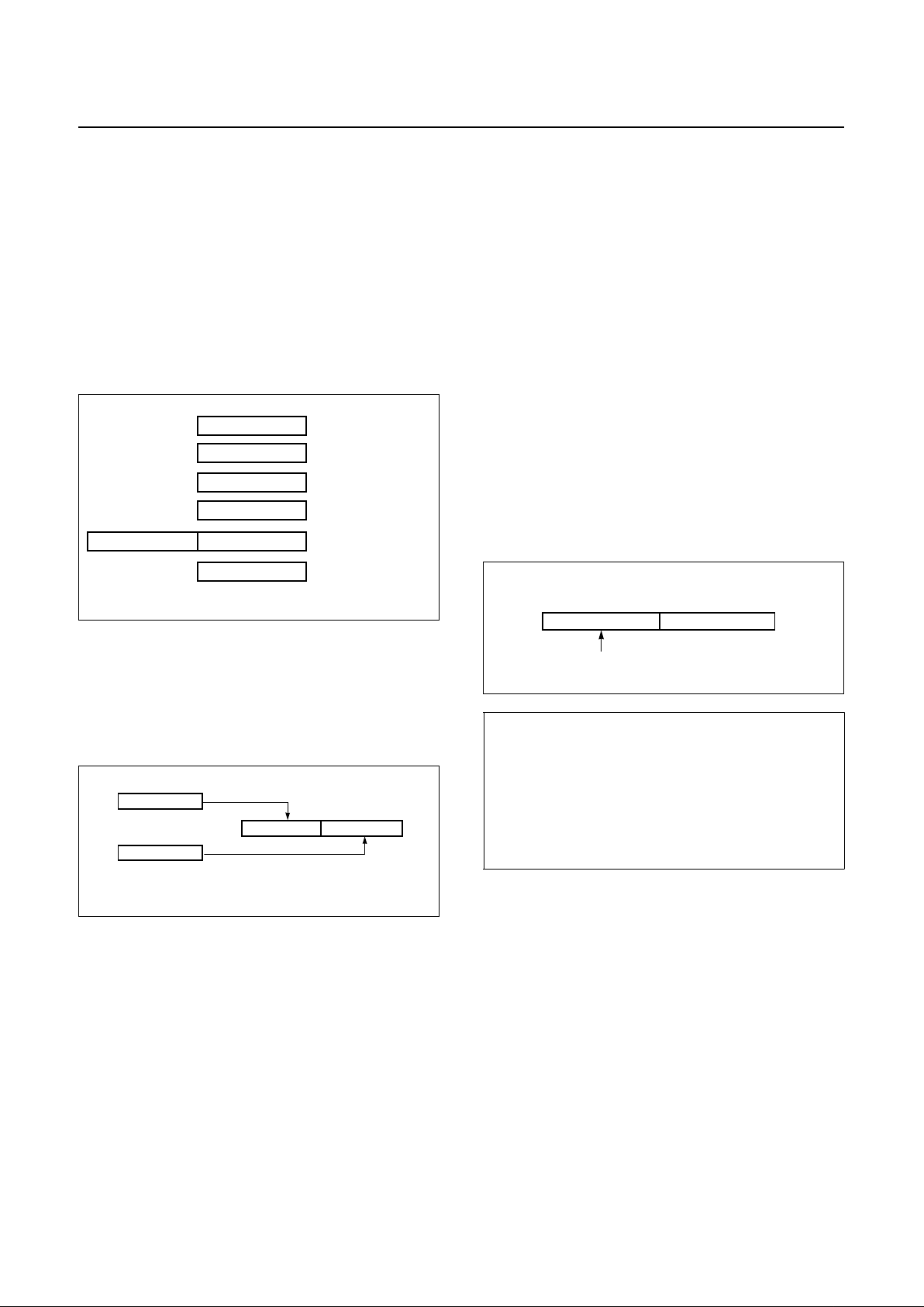
8.1 Registers
This device has six registers that are the Program Counter
(PC), a Accumulator (A), two index registers (X, Y), the
Stack Pointer (SP), and the Program Status Word (PSW).
The Program Counter consists of 16-bit register .
Figure 8-1 Configuration of Registers
Accumulator:
The Accumulator is the 8-bit general purpose register, use d for data opera tio n such as tr ansfer , temporary saving, an d conditional judgement, etc.
The Accumulator can be used as a 16-bit register with Y
Register as shown below.
Figure 8-2 Configurati on of YA 16-bit Register
X, Y Registers
: In the addressing mode which uses these
index registers , the regist er contents are a dded to the specified addr ess, which be comes the act ual address. The se
modes are extremely effective for referencing subroutine
tables and memory table s. The index re gisters al so have increment, decrement, comparison and data transfer functions, and they can be used as simple accumulators.
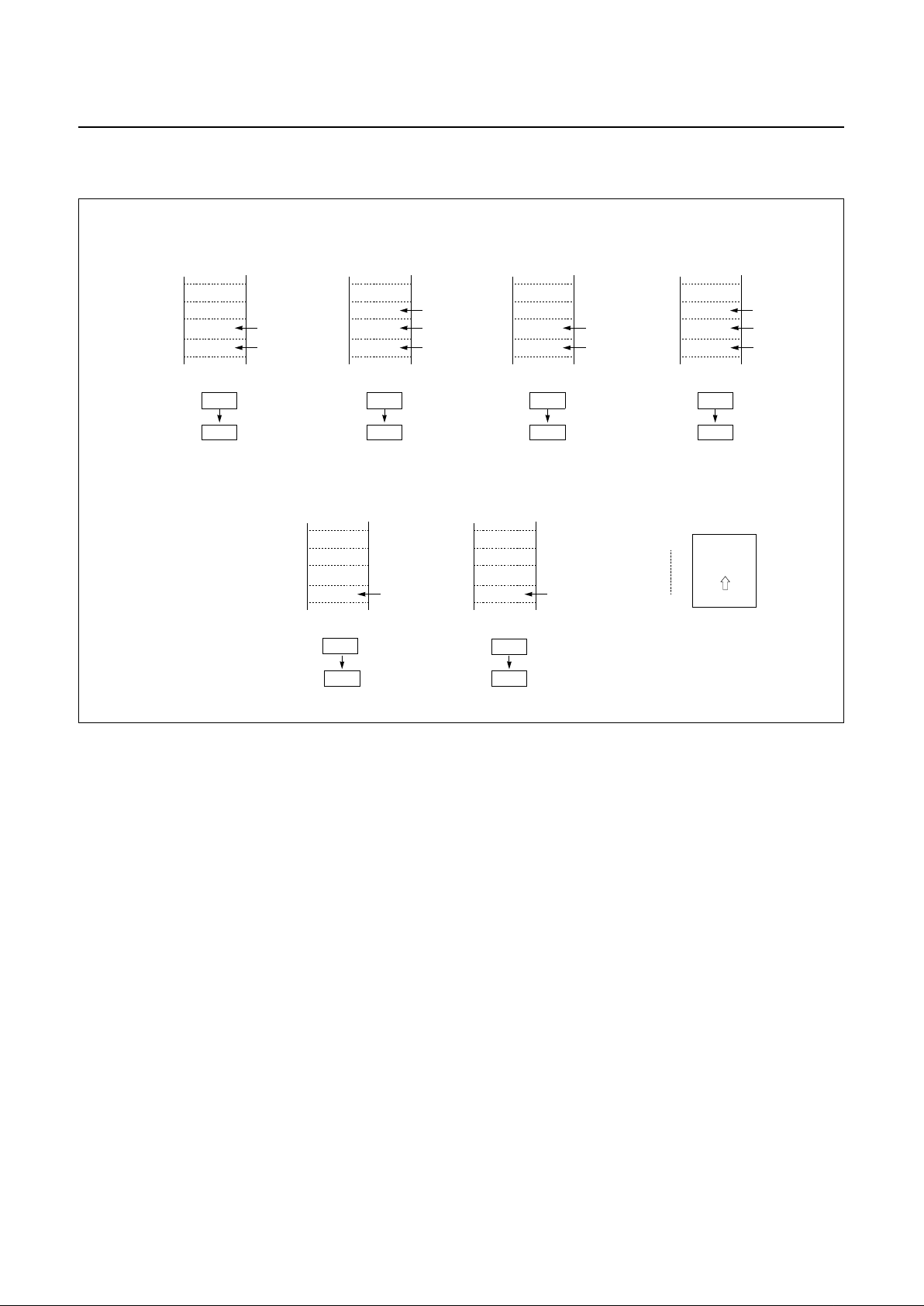
Stack Pointer
: The Sta ck Poi nte r is an 8-b it re gist er us ed
for occurrence inte rrupts and calling ou t subrouti nes. Stack
Pointer identifies the location in the stack to be accessed
(save or restor e).
Generally, SP is automatically updated when a subroutine
call is executed or an interrupt is accepted. However, if it
is used in excess of the stack area permitted by the data
memory allocating configuration, the user-processed data
may be lost.
The stack can be located at any position within 0100
H
to
01FF
H
of the internal data memory. The SP is not initialized by hardware, requiring to write the initial value (the
location wit h whi ch the use of the stac k st arts) by u sing t he
initialization routine. Normally, the initial value of "FF
H
"
is used.
Program Counter
: The Program Counter is a 16-bit wi de
which consists of two 8-bit registers, PCH and PCL. This
counter indicates the address of the next instruction to be
executed. In reset state, the pr o g ram cou n ter has r eset routine address (PC
H
:0FFH, PCL:0FEH).
Program Status Word
: The Program Status Word (PSW)
contains several bits that reflect the current state of the
CPU. The PSW is described in Figure 8-3 . It contains the
Negative flag, the Overflow flag, the Break flag the Half
Carry (for BCD operation), the Interrupt enable flag, the
Zero flag, and the Carry flag.
[Carry flag C]
This flag stores a ny carry o r borro w from the ALU of CPU
A
ACCUMULATOR
X REGISTER
Y REGISTER
STACK PO INT ER
PROGRAM COUNTER
PROGRAM STATUS
WORD
X
Y
SP
PCLPCH
PSW
Two 8-bit Registers can be used as a "YA" 16-bit Register
Y
A
Y A
Caution:
The Stack Pointer must be initialized by software be-
cause its value is un d ef ined aft er RESET.
Example: To initialize the SP
LDX #0FFH
TXSP ; SP ← FF
H
SP
01
Stack Address ( 0100
H
~ 01FFH )
15 087
Hardware fixed
GMS81C4040/87C4060
PRELIMINARY
18
PRELIMINARY
Nov. 1999 Ver 1.0
after an arithmetic operation and is also changed by the
Shift Instruction or Rotate Instruction.
Figure 8-3 PSW (Program Status Wo rd) Register
[Zero flag Z]
This fl ag is set when the re sult of an arith metic op erat ion
or data transfer is "0" and is cleared by any other result.
[Interrupt disable flag I]
This flag enables/disables all interrupts except interrupt
caused by Reset o r software BRK in struction. All interrupts are disabled when cleared to "0". This flag immediately becomes "0" when an interrupt is served. It is set by
the EI instruction and cleared by the DI instruction.
[Half carry flag H]
After operation, this is set when there is a carry from bit 3
of ALU or there is borrow from bit 4 of ALU. This bit can
not be set or cleared except CLRV instruction with Overflow flag (V).
[Break flag B]
This flag is set by software BRK instruct ion to distinguish
BRK from TCA LL instruction with the s ame vector address.
[Direct page flag G]
This flag a ssigns RAM pa ge for dire ct a ddres sing mode. In
the direct addressing mode, addressing area is from zero
page 00
H
to 0FFH when this flag is "0". If it is set to "1",
addressing area is assigned by DPGR register (address
0F8
H
). It is set by SETG i nstru ction a nd clear ed by CL RG.
[Overflow flag V]
This flag is set to "1" when an overflow occurs as the result
of an arithmetic operation involving signs. An overflow
occurs when the r esult of an add ition or s ubtraction exceeds + 127(7F
H
) or -128(80H). The CLRV instruction
clears the overflow flag. There is no set instruction. When
the BIT instruction is executed, bit 6 of memory is copied
to this flag.
[Nega tiv e f la g N ]
This flag is set to match the sign bit (bit 7) status of the re-
sult of a data or arithmetic operation. When the BIT instruction is execu ted, bit 7 of memor y is copied to this fla g.
N
NEGATIVE FLAG
V G B H I Z C
MSB LSB
RESET VALUE : 00
H
PSW
OVERFLOW FLAG
BRK FLAG
CARRY FLAG RECEIVES
ZERO FLAG
INTERRUPT ENABLE FLAG
CARRY OUT
HALF CARRY FLAG RECEIVES
CARRY OUT FROM BIT 1 OF
ADDITION OPERLANDS
SELECT DIRECT PAGE
when G=1, page is addressed by RPR
PRELIMINARY
GMS81C4040/87C4060
Nov. 1999 Ver 1.0
PRELIMINARY
19
Figure 8-4 Stack Operation
At execution of
a CALL/TCALL/PCALL
PCL
PCH
01FF
SP after
execution
SP before
execution
01FD
01FE
01FD
01FC
01FF
Push
down
At acceptance
of interrupt
PCL
PCH
01FF
01FC
01FE
01FD
01FC
01FF
Push
down
PSW
At execution
of RET instruction
PCL
PCH
01FF
01FF
01FE
01FD
01FC
01FD
Pop
up
At execution
of RETI instruction
PCL
PCH
01FF
01FF
01FE
01FD
01FC
01FC
Pop
up
PSW
0100H
01FFH
Stack
depth
At execution
of PUSH in struction
A
01FF
01FE
01FE
01FD
01FC
01FF
Push
down
SP after
execution
SP before
execution
PUSH A (X,Y,PSW)
At execution
of POP instruction
A
01FF
01FF
01FE
01FD
01FC
01FE
Pop
up
POP A (X,Y,PSW)
GMS81C4040/87C4060
PRELIMINARY
20
PRELIMINARY
Nov. 1999 Ver 1.0
8.2 Program Memory
A 16-bit program counter is capable of addressing up to
64K bytes, but GMS81C4040/GMS87C4060 has 40K/
60K bytes program memory space only physically implemented. Accessing a location above FFFF
H
will cause a
wrap-around to 0000
H
.
Figure 8-5 , shows a map of Pro gram Memory. Aft er reset,
the CPU begins e xecution from reset vect or which is stored
in address FFFE
H
and FFFFH as shown in Figure 8-6 .
As shown in Figure 8-5 , each area is assigned a fixed location in Program Memory. Progr am Memory area c ontains the user program.
Figure 8-5 Program Memory Map
Page Call (PCALL) area contains subroutine program to
reduce program byte length by using 2 bytes PCALL instead of 3 bytes CALL instr uction. If it is frequent ly called ,
it is more useful to save program byte length.
Table Call (TCALL) causes the CPU to jump to each
TCALL address, where it commences the execution of the
serv ic e r ou t in e. Th e Tab l e Call servic e area space s 2 - b y te
for every TCALL: 0FFC0
H
for TCALL15, 0FFC2H for
TCALL14, etc., as shown in Figure 8-7 .
Example: Usage of TCALL
The in terrup t cau s es the CP U to ju m p to s p ec if ic loca t i on ,
where it comm ence s the ex ecuti on of th e serv ice ro utine.
The External interrupt 0, for example, is assigned to location 0FFFC
H
. The in terr up t se rvic e lo catio ns spa ces 2-by te
interval: 0FFF8
H
and 0FFF9H for Ex terna l Interr upt 1,
0FFFC
H
and 0FFFDH for External Interrupt 0, etc.
Any area from 0FF00
H
to 0FF FFH, if it is not going to be
used, its service location is available as general purpose
Program Memory.
Figure 8-6 Interr upt Vector Area
PROGRAM
MEMORY
TCALL
AREA
INTERRUPT
VECTOR AREA
81C4040:6000H
FEFFH
FF00H
FFC0H
FFDFH
FFE0H
FFFFH
PCALL
AREA
81C4060:1000H
FFBFH
LDA #5
TCALL 0FH ;
1BYTE INSTRUCTION
:;
INSTEAD OF 2 BYTES
:;
NORMAL CALL
;
;TABLE CALL ROUTINE
;
FUNC_A: LDA LRG0
RET
;
FUNC_B: LDA LRG1
RET
;
;TABLE CALL ADD. AREA
;
ORG 0FFC0H ;
TCALL ADDRESS AREA
DW FUNC_A
DW FUNC_B
1
2
0FFE0
H
E2
Address Vector Area Memory
E4
E6
E8
EA
EC
EE
F0
F2
F4
F6
F8
FA
FC
FE
I
2
C Bus Interface Interrupt Vector Area
Serial I/O Interrupt Vector Area
Basic Interval Timer Interrupt Vector Area
Watchdog Timer Interrupt Vector Area
Timer/Counter 3 Interrupt Vector Area
Timer/Counter 1 Interrupt Vector Area
V-Sync Interrupt Vector Area
Timer/Counter 2 Interrupt Vector Area
Timer/Counter 0 Interrupt Vector Area
External Interrupt 2 Vector Area
On Screen Display Interrupt Vector Area
External Interrupt 0 Vector Area
RESET Vector Area
External Interrupt 1 Vector Area
1 Frame Timer Interrupt Vector Area
External Interrupt 3/4 Vector Area
"-" means reserved area.
NOTE:
PRELIMINARY
GMS81C4040/87C4060
Nov. 1999 Ver 1.0
PRELIMINARY
21
Figure 8-7 PCALL and TCALL Memory Area
PCALL→
→ →
→ rel
4F35 PCALL 35H
TCALL →
→ →
→ n
4A TCALL 4
0FFC0
H
C1
Address Program Memory
C2
C3
C4
C5
C6
C7
C8
0FF00
H
Address PCALL Area Memory
0FFBF
H
PCALL Area
(192 Bytes)
* means that the BRK software interrupt is using
same address with TCALL0.
NOTE:
TCALL 15
TCALL 14
TCALL 13
TCALL 12
TCALL 11
TCALL 10
TCALL 9
TCALL 8
TCALL 7
TCALL 6
TCALL 5
TCALL 4
TCALL 3
TCALL 2
TCALL 1
TCALL 0 / BRK *
C9
CA
CB
CC
CD
CE
CF
D0
D1
D2
D3
D4
D5
D6
D7
D8
D9
DA
DB
DC
DD
DE
DF
4F
~
~
~
~
Sub-routine
35
0FF35H
0FF00H
0FFFFH
Upper address is
assumed 0FF
H.
11111111
11010110
01001010
PC:
FHFHDH6
H
4A
~
~
~
~
25
0FFD6H
0FF00H
0FFFFH
D1
Sub-routine
0FFD7H
þ
À
Ã
0D125H
Reverse

GMS81C4040/87C4060
PRELIMINARY
22
PRELIMINARY
Nov. 1999 Ver 1.0
Example: The usage software example of Vector address and the initialize part.
ORG 0FFE0H
DW I2C ; I2C
DW SERIAL ; Serial I/ O
DW BIT ; Basic interval timer
DW WATCHDOG ; Watch dog timer
DW INT3_4 ; Interrupt 3/4
DW TIMER3 ; Timer 3
DW TIMER1 ; Timer 1
DW VSYNC ; Vertica l Sy nc .
DW One_Frame ; 1 Frame interrupt
DW TIMER2 ; Timer 2
DW TIMER0 ; Timer 0
DW INT2 ; Interrupt 2
DW INT1 ; Interrupt 1
DW OSD ; On Screen Display
DW INT0 ; Interrupt 0
DW RESET ; Reset
ORG 0F000H
;****** ** ** ** ****** ** *** ** ** ************* ** **
; MAIN PROGRAM *
;********************************************
;
RESET: DI ; Disable All Interrupts
LDX #0
LDA #0 ; RAM Clear(!0000H->!00BFH)
RAM_CLR: STA {X}+
CMPX #0C0H
BNE RAM_CLR
;
CALL LCD_CLR ; Clear LCD display memory
;
LDX #03FH ; Stack Pointer Initialize
TXSP
LDM R0, #0 ; Normal Port 0
LDM R0DD,#1000_0010B ; Normal Port Direction
:
:
:
:
PRELIMINARY
GMS81C4040/87C4060
Nov. 1999 Ver 1.0
PRELIMINARY
23
8.3 Data Memory
Figur e 8- 8 sho w s th e i nt er n a l D at a M emory sp ac e av ailable. Data Memory is di vided into four groups, a user RAM,
control registers, Stack, and OSD memory.
Figure 8-8 Data Memory Map
User Memory
The GMS81C4040/GM S87C4060 has 1,536 × 8 bits for
the user memory (RA M ).
Control Registers
The control registers are used by the CPU and Peripheral
function blocks for controlling the desired operat ion of the
device. Theref ore these regis ters contai n contr ol a nd sta tus
bits for the interru p t system, th e timer/ coun ters, analog to
digital conv ert ers and I /O po rts. The ba sic co ntro l regis t ers
are in address range of 00C0
H
to 00FFH. And OSD control
registers are assigned within 0AE0
H
~ 0AFFH.
Note that unoccupied addresses may not be implemented
on the chip . Re ad ac ce sse s to t hese add ress es w ill in g eneral return random data, and write accesses will have an indeterminate effect.
More detailed informations of each register are explained
in each peripheral section.
Note:
Write only registers can not be accessed by bit manipulation inst ruct ion . Do not use read- modi fy-wr ite i nstruc tion. Use byte manipulation instruction.
Example; To write at CKCTLR
LDM CLCTLR,#09H ;Divide ratio ÷8
Stack Area
The stack pro vides the area where the return address is
saved before a jump is performed du ring the pro cessing
routine at the execution of a subroutine call instruction or
the acceptance of an in terrupt.
When returning from the processing routine, executing the
subroutine re turn inst ruction [RET ] restores t he contents of
the program counter fro m the stack; executing the int errupt
return instruction [RETI] restores the contents of the program counter and flags.
The save/restore locations in the stack are determined by
the stack pointed (SP). The SP is automatically decreased
after the saving, and increased before the restoring. This
means the value of the SP indicates the stack location
number for the next save. Refer to Figure 8-4 on page 19.
Page0
RAM (192 bytes)
Peripheral Reg. (64 bytes)
0100H
00C0H
0000H
RAM (256 bytes)
0200H
RAM (256 bytes)
0300H
RAM (256 bytes)
0400H
RAM (256 bytes)
0500H
RAM (256 bytes)
0600H
RAM (64 bytes)
0A00H
OSD RAM (192 bytes)
0AE0H
Peripheral Reg. (32 bytes)
0C00H
Sprite RAM (96 bytes)
Empty area
Page1
Page2
Page3
Page4
Page5
Page6
PageA
PageC
063FH
Stack area
0C5FH
Address Symbol R/W Reset Value
Addressing
mode
00C0H
00C1H
00C2H
00C3H
00C4H
00C5H
00C8H
00C9H
00CAH
00CBH
00CCH
00CDH
00CEH
00CFH
R0
R0DD
R1
R1DD
R2
R2DD
R4
R4DD
R5
R5DD
R6
R6DD
FUNC1
FUNC2
R/W
W
R/W
W
R/W
W
R/W
W
R/W
W
R/W
W
W
W
????????
00000000
????????
00000000
????????
00000000
????????
0000---????????
----0000
?------0-------
-0000000
---00000
byte, bit
1
byte
2
byte, b it
byte
byte, b it
byte
byte, b it
byte
byte, b it
byte
byte, b it
byte
byte
byte
Table 8-1Control reg isters

GMS81C4040/87C4060
PRELIMINARY
24
PRELIMINARY
Nov. 1999 Ver 1.0
0D0H
0D1H
0D2H
0D3H
0D4H
0D5H
0D6H
0D7H
0D8H
0D9H
0DAH
0DBH
0DCH
0DEH
0DFH
TM0
TM2
TDR0
TDR1
TDR2
TDR3
BITR
CKCTLR
WDTR
ICAR
ICDR
ICSR
ICCR1
ICCR2
SIOM
SIOR
R/W
R/W
R/W
R/W
R/W
R/W
R
W
W
R/W
R/W
R/W
R/W
R/W
R/W
R/W
-0000000
-0000000
????????
????????
????????
????????
????????
--010111
-0111111
00000000
11111111
000100000000000
00000000
-0000001
????????
byte
byte
byte, bi t
byte, bi t
byte, bi t
byte, bi t
byte
byte
byte
byte, bi t
byte, bi t
byte, bi t
byte, bi t
byte, bi t
byte, bi t
byte, bi t
0E0H
0E1H
0E2H
0E3H
0E4H
0E5H
0E8H
0E9H
0EAH
0EBH
0EEH
0EFH
PWMR0
PWMR1
PWMR2
PWMR3
PWMR4
PWMR5
PWM8H
PWM8L
PWMCR1
PWMCR2
BUR
AIPS
W
W
W
W
W
W
R/W
R/W
R/W
R/W
W
W
????????
????????
????????
????????
????????
????????
????????
--??????
00000000
--0-0000
????????
--000000
byte
byte
byte
byte
byte
byte
byte, bi t
byte, bi t
byte, bi t
byte, bi t
byte
byte
0F0H
0F1H
0F2H
0F3H
0F4H
0F5H
0F6H
0F7H
0F9H
0FAH
0FBH
0FCH
0FDH
ADCM
ADR
IEDS
IMOD
IENL
IRQL
IENH
IRQH
IDCR
IDFS
IDR
DPGR
TMR
R/W
R
W
R/W
R/W
R/W
R/W
R/W
R/W
R
R
R/W
W
--011101
????????
--000000
--000000
0000000000000000000000
00000000
0000-000
1----001
????????
----0000
????????
byte, bi t
byte
byte
byte, bi t
byte, bi t
byte, bi t
byte, bi t
byte, bi t
byte, bi t
byte
byte
byte, bi t
byte
0AE0H
0AE1H
0AE2H
0AE3H
0AE4H
0AE5H
0AE6H
0AE8H
0AE9H
0AF0H
0AF1H
0AF3H
0AF4H
OSDcon1
OSDcon2
OSDPOL
FDWSET
EDGEcol
OSDLN
LHPOS
SPVPOS
SPHPOS
L1ATTR
L1VPOS
L2ATTR
L2VPOS
R/W
R/W
W
W
W
R
W
W
W
W
W
W
W
00000000
-0000000
????????
01111010
10000111
---00000
????????
????????
????????
????????
????????
????????
????????
byte, bi t
byte, bi t
byte
byte
byte
byte
byte
byte
byte
byte
byte
byte
byte
Table 8-1Control registers
1. "byte, bit" means that register can be addressed by not only bit
but byt e manipulation instruction.
2. "byte" means that register can be addressed by only byte
manipulation instruction. On the other hand, do not use any
read-modify-write instruction such as bit manipulation for clearing bit .

PRELIMINARY
GMS81C4040/87C4060
Nov. 1999 Ver 1.0
PRELIMINARY
25
8.4 Addressing Mode
The GMS800 series uses six addressing modes;
• Register addressing
• Immediate addressing
• Direct page addressing
• Absolute addressing
• Indexed addressing
• Register-indirect addressing
(1) Register Addressing
Register addressin g accesses the A, X, Y, C and PSW.
(2) Immediate Addressing →
→ →
→ #imm
In this mode, second byte (operand) is accessed as a data
immed iatel y.
Exam ple:
FE10: 0435 ADC #35H
When G-flag is 1, then RAM address is defined by 16-bit
address which is composed of 8-bit direct page accessable
register (DPGR) and 8-bit immediate data.
Example: G=1, DPGR=0CH
F100: E45535 LDM 35H,# 55H
(3) Direct Page Addressing →
→ →
→ dp
In this mode, a address is specified within direc t page.
Example; G=0
E551: C5 35 LDA 35H;A ←RAM[35H]
(4) Absolute Addressing →
→ →
→ !abs
Absolute addr essing sets corr esponding memor y data to
Data , i.e. second byte(Operand I) of command becomes
lower level address and third byte (Operand II) becomes
upper level address.
With 3 bytes command, it is possible to access to whole
memory area.
ADC, AND, CMP, CMPX, CMPY, EOR, LDA, LDX,
LDY, OR, SBC, STA, STX, STY
Example;
F100: 07 35 F0 ADC!0F 035H ;A ←ROM[0F035H]
35
A+35H+C → A
04
MEMORY
0FE10
H
E4
0F100
H
data
←
55H
~
~
~
~
data
0C35
H
þ
35
0F102
H
550F101
H
A
data
35
35
H
0E551
H
data → A
À
þ
~
~
~
~
C5
0E550
H
07
0F100
H
~
~
~
~
data0F035
H
P
F0
0F102
H
350F101
H
A
A+data+C → A
address: 0F035
GMS81C4040/87C4060
PRELIMINARY
26
PRELIMINARY
Nov. 1999 Ver 1.0
The operation within data memory (RAM)
ASL, BIT, DEC, INC, LSR, ROL, ROR
Exam ple; A dd res sing ac cesses t he a ddre ss 0 135
H
regard-
less of G-flag and DPGR.
F100: 983501 INC!0135H ;A ←ROM[135H]
(5) Indexed Addressing
X indexe d di rec t pa g e (no of f set ) →
→ →
→ {X}
In this mode, a address is specified by the X register.
ADC, AND, CMP, EOR, LDA, OR, SBC, STA, XMA
Example; X=15
H
, G=1, DPGR=03
H
E550: D4 LDA {X};ACC←RAM[X].
X indexed direct page, auto increment→
→ →
→ {X}+
In this mode, a address is specified within direct page by
the X register and the content of X is increased by 1.
LDA, STA
Example; G=0, X=35
H
F100: DB LDA {X}+
X indexed direct page (8 bit offset) →
→ →
→ dp+X
This address value is the second byte (Operand) of command plus the data of -register. And it assigns the memory in Direct page.
ADC, AND, CMP, EOR , LDA, LDY, OR, SBC, STA
STY, XMA, ASL, D EC, INC, LSR, ROL, RO R
Example; G=0, X=0F5
H
E550: C6 45 LDA 45H+X
98
0F100
H
~
~
~
~
data135
H
þ
01
0F102
H
350F101
H
À
data+1 → data
Ã
address: 0135
data
D4
315
H
0E550
H
data → A
À
þ
~
~
~
~
data
DB
35
H
data → A
À
þ
~
~
~
~
36H → X
0F100
H
data
45
3A
H
0E551
H
data → A
À
þ
~
~
~
~
C6
0E550
H
45H+0F5H=13AH
Ã
 Loading...