

HEI GMS81604, GMS81608TPL, GMS81608TK, GMS81608T, GMS81608PL Datasheet
...
LG Semicon
8-bit Microcontrollers
GMS81604/08
Revision History
Rev 1.2 (Dec. 1998)
Redraw package dimension on page 5~6.
Rev 1.1 (Nov. 1998)
Operating Voltage, 2.7~5.5V is extended with 2.4~5.5V.
Operating Temperature, -20~80°C is extended wi t h -20~85°C.
Add the "Typical Characteristics" on page 16, 17.
Add the unused port guidance on page 48.
Revision the information for the OTP programming guidance, recommand using "Intelligent Mode" on page 49.
Add the chapter for OTP programming specification as an appendix.
Rev 1.0 (Nov. 1997)
First Edition

Second Edition
Published by
MCU Application Team
1998 LG Semicon Co., Ltd. All right reserved.
Additional information of this manual may be served by LG Semicon offices in Korea or Distributors and
Representatives listed at address directory.
LG Semicon reserves the right to make changes to any information here in at any time without notice.
The information, diagrams and other data in this manual are correct and reliable; however, LG Semicon Co,. Ltd.
is in no way responsible for any violations of patents or other rights of the third party generated by the use of this
manual.

Table of Contents
OVERVIEW . . . . . . . . . . . . . . . . . . . . . . . . . . . . . . . . . . . . . . . . . . . . . . 1
BLOCK DIAGRAM . . . . . . . . . . . . . . . . . . . . . . . . . . . . . . . . . . . . . . . . . . 3
PIN ASSIGNMENT . . . . . . . . . . . . . . . . . . . . . . . . . . . . . . . . . . . . . . . . . . 4
PACKAGES . . . . . . . . . . . . . . . . . . . . . . . . . . . . . . . . . . . . . . . . . . . . . . 5
PIN DESCRIPTIONS . . . . . . . . . . . . . . . . . . . . . . . . . . . . . . . . . . . . . . . . . 7
PORT STRUCTURES . . . . . . . . . . . . . . . . . . . . . . . . . . . . . . . . . . . . . . . . 9
ELECTRICAL CHARACTERISTICS . . . . . . . . . . . . . . . . . . . . . . . . . . . . . . . . . 12
MEMORY ORGANIZATION . . . . . . . . . . . . . . . . . . . . . . . . . . . . . . . . . . . . . 18
Registers . . . . . . . . . . . . . . . . . . . . . . . . . . . . . . . . . . . . . . . . . . . . . 18
Program Memory . . . . . . . . . . . . . . . . . . . . . . . . . . . . . . . . . . . . . . . . . 20
Data Memory . . . . . . . . . . . . . . . . . . . . . . . . . . . . . . . . . . . . . . . . . . . 21
I/O PORTS . . . . . . . . . . . . . . . . . . . . . . . . . . . . . . . . . . . . . . . . . . . . . . 23
BASIC INTERVAL TIMER . . . . . . . . . . . . . . . . . . . . . . . . . . . . . . . . . . . . . . 26
TIMER/COUNTER . . . . . . . . . . . . . . . . . . . . . . . . . . . . . . . . . . . . . . . . . . 27
8-bit Timer/Counter Mode . . . . . . . . . . . . . . . . . . . . . . . . . . . . . . . . . . . . 29
16-bit Timer/Counter Mode . . . . . . . . . . . . . . . . . . . . . . . . . . . . . . . . . . . 31
8-bit Capture Mode . . . . . . . . . . . . . . . . . . . . . . . . . . . . . . . . . . . . . . . . 32
16-bit Capture Mode . . . . . . . . . . . . . . . . . . . . . . . . . . . . . . . . . . . . . . . 33
ANALOG TO DIGITAL CONVERTER . . . . . . . . . . . . . . . . . . . . . . . . . . . . . . . . 34
How to Use A/D Converter . . . . . . . . . . . . . . . . . . . . . . . . . . . . . . . . . . . 34
BUZZER FUNCTION . . . . . . . . . . . . . . . . . . . . . . . . . . . . . . . . . . . . . . . . . 36
INTERRUPTS . . . . . . . . . . . . . . . . . . . . . . . . . . . . . . . . . . . . . . . . . . . . . 37
External Interrupt . . . . . . . . . . . . . . . . . . . . . . . . . . . . . . . . . . . . . . . . 38
BRK Interrupt . . . . . . . . . . . . . . . . . . . . . . . . . . . . . . . . . . . . . . . . . . . 40
Multiple Interrupt . . . . . . . . . . . . . . . . . . . . . . . . . . . . . . . . . . . . . . . . . 40
WATCHDOG TIMER . . . . . . . . . . . . . . . . . . . . . . . . . . . . . . . . . . . . . . . . . 41

STOP MODE . . . . . . . . . . . . . . . . . . . . . . . . . . . . . . . . . . . . . . . . . . . . . 42
Release Stop Mode . . . . . . . . . . . . . . . . . . . . . . . . . . . . . . . . . . . . . . . 42
Minimizing Current Consumption in Stop Mode . . . . . . . . . . . . . . . . . . . . . . . . 43
RESET . . . . . . . . . . . . . . . . . . . . . . . . . . . . . . . . . . . . . . . . . . . . . . . . 44
POWER FAIL PROCESSOR . . . . . . . . . . . . . . . . . . . . . . . . . . . . . . . . . . . . . 45
OSCILLATOR CIRCUIT . . . . . . . . . . . . . . . . . . . . . . . . . . . . . . . . . . . . . . . 47
UNUSED PORTS . . . . . . . . . . . . . . . . . . . . . . . . . . . . . . . . . . . . . . . . . . . 48
GMS81608T (OTP) PROGRAMMING . . . . . . . . . . . . . . . . . . . . . . . . . . . . . . . . 49
1. Using the Universal programmer . . . . . . . . . . . . . . . . . . . . . . . . . . . . . . 49
2. Using the general EPROM(27C256)
programmer . . . . . . . . . . . . . . . . . . . . . . . . . . . . . . . . . . . . . . . . . . 49
GMS81608T PROGRAMMING MANUAL . . . . . . . . . . . . . . . . . . . . . . . . . . . . . . 50
APPENDIX
A. INSTRUCTION SET
B. MASK ORDER SHEET
LG Semicon GMS81604/08
GMS81604 / GMS81608
CMOS SINGLE-CHIP 8-BIT MICROCONTROLLER
OVERVIEW
Description
The GMS81604/08 is a high-performance CMOS 8-bit microcontroller with 4K or 8K bytes of ROM. The device
is one of GMS800 family. The LG Semicon GMS81604/08 is a powerful microcontroller which provides a highly
flexible and cost effective solution to many embedded control applications. The GMS81604/08 provides the
following standard features: 8K bytes of ROM, 256 bytes of RAM, 35 I/O lines(33 lines for 40PDIP), 16-bit or
8-bit timer/counter, a precision analog to digital converter, on-chip oscillator and clock circuitry. In addition, the
GMS81604/08 supports power saving modes to reduce power consumption. The Stop Mode saves the RAM
contents but freezes the oscillator disabling all other chip functions until the next hardware reset or external
interrupt.
Features
4K/ 8K On-chip Program Memory
256 Bytes of On-Chip Data RAM
Instruction execution time: 0.5us at 8MHz
2.4V to 5.5V Operating Range
1~8 MHz Operating frequency
Basic Interval Timer
Four 8-Bit Timer/ Counters (can be used
as two 16-bit)
Four external interrupt ports
Two Programmable Clock Out
Memory Proliferation
Device ROM Bytes RAM Bytes
GMS81604 4K 256
GMS81608 8K 256
GMS81608T 8K EPROM 256
Development Tools
The GMS800 family is supported by a full-featured
macro assembler, an in-circuit emulators CHOICEJr.TM, socket adapters for OTP device.
The availability of OTP devices are especially useful
for customers expecting frequent code changes and
updates. The OTP devices, packaged in plastic pack-
One Buzzer Driving port
31 Programmable I/O, 4 Input pins,
Twelve Interrupt Sources
All LED Direct Drive Output Ports
8-Channel 8-Bit On-Chip Analog to Digital
Converter
Power Fail Processor
(Noise immunity circuit)
Power Down Mode (Stop Mode)
ages permit the user to program them once. In addition
to the program memory, the configuration fuses must
be programmed.
GMS81604, GMS81608
In-Circuit
Emulators
OTP devices GMS81608T (40 DIP)
Socket
Adapters for
OTP Devices
Assembler LGS Macro Assembler
CHOICE-Jr.
GMS81608T K (42 SDIP)
GMS81608T PL (44 pin PLCC)
OA816A-40PD (40 DIP)
OA816A-42SD (42 SDIP)
OA816A-44PL (44 PLCC)
TM
1
GMS81604/08 LG Semicon
Device Selection Guide
ROM size Package Ordering code
4K bytes 40DIP GMS81604
42SDIP GMS81604 K
44PLCC GMS81604 PL
8K bytes 40DIP GMS81608
42SDIP GMS81608 K
44PLCC GMS81608 PL
8K bytes (OTP) 40DIP GMS81608T
42SDIP GMS81608T K
44PLCC GMS81608T PL
2
LG Semicon GMS81604/08
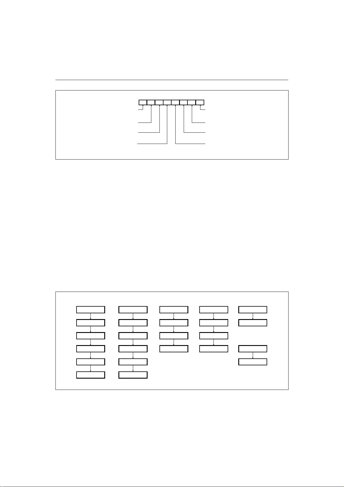
BLOCK DIAGRAM
Figure 1. Block Diagram
3
GMS81604/08 LG Semicon
PIN ASSIGNMENT
PACKAGES
Part Package Type
GMS8160X
GMS8160X K
GMS8160X PL
42 SDIP
40DIP
42SDIP
44PLCC
40 PDIP
44 PLCC
Figure 2. Pin Connections
← "X" means 4(4K bytes) or 8(8K bytes).
4
LG Semicon GMS81604/08
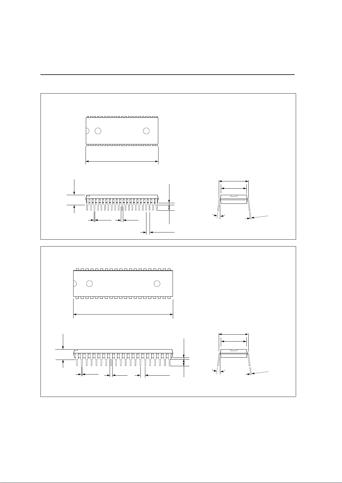
PACKAGE
42SDIP
UNIT: INCH
1.470
1.450
0.600 BSC
0.550
0-15
0.530
2
1
0
.
0
8
0
0
.
°
0
0.190 max.
min. 0.015
0.020
0.016
0.045
0.035
0.140
0.070 BSC
0.120
40DIP
UNIT: INCH
2.075
2.045
0.600 BSC
0.550
0-15
0.530
2
1
0
.
0
8
0
0
.
°
0
5
0.200 max.
0.022
0.015
0.065
0.045
0.100 BSC
min. 0.015
0.140
0.120
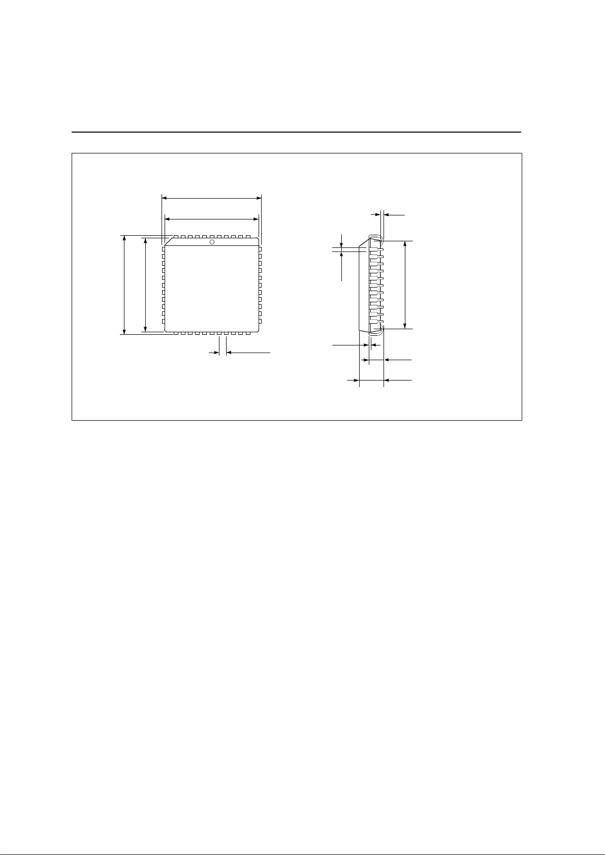
GMS81604/08 LG Semicon
44PLCC
UNIT: INCH
0.695
0.685
min. 0.020
0.630
0.590
0.695
0.685
0.656
0.650
0.656
0.650
0.032
0.026
0.050 BSC
0.012
0.0075
0.120
0.090
0.180
0.165
6
LG Semicon GMS81604/08
PIN DESCRIPTIONS
V
: Supply voltage.
DD
V
: Circuit Ground.
SS
TEST: For test purposes only. Connect it to V
DD
.
RESET: Reset the MCU.
X
: Input to the inverting oscillator amplifier and
IN
input to the internal clock operating circuit.
X
: Output from the inverting oscillator amplifier.
OUT
R00~R07: R0 is an 8-bit, CMOS, bidirectional I/O
port. As an output port each pin can sink several LS
TTL inputs. R0 pins that have 1 or 0 written to their
Port Direction Mode Register, can be used as outputs
or inputs.
R10~R17: R1 is an 8-bit, CMOS, bidirectional I/O
port. As an output port each pin can sink several LS
TTL inputs. R1 pins that have 1 or 0 written to their
Port Direction Mode Register, can be used as outputs
or inputs.
R40~R47: R4 is an 8-bit, CMOS, bidirectional I/O
port. As an output port each pin can sink several LS
TTL inputs. R4 pins that have 1 or 0 written to their
Port Direction Mode Register, can be used as outputs
or inputs.
In addition, Port 4 serves the functions of the various
following special features.
Port Pin Alternate Function
R40 INT0 (External Interrupt 0)
R41 INT1 (External Interrupt 1)
R42
R43
R44
R45
R46
R47
INT2 (External Interrupt 2)
INT3 (External Interrupt 3)
EC0 (External Count Input to Timer/
Counter 0)
EC2 (External Count Input to Timer/
Counter 2)
T1O (Timer 1 Clock-Out)
T3O (Timer 3 Clock-Out)
R50, R51, R55: R5 is a 3-bit, CMOS, bidirectional I/O
port. As an output port each pin can sink several LS
TTL inputs. R5 pins that have 1 or 0 written to their
Port Direction Mode Register, can be used as outputs
or inputs. R50 and R51 differs in having internal
pull-ups.
Port R55 serves the functions of special features.
Port Pin Alternate Function
R55 BUZ (Square wave output for Buzzer
driving)
R60~R67: R6 is an 8-bit, CMOS, I/O port. R60~R63
can be used as only input, can not be output, R64~R67
are bidirectional I/O port. As an output port each pin
can sink several LS TTL inputs. R64~R67 pins that
have 1 or 0 written to their Port Direction Mode
Register, can be used as outputs or inputs.
R6 serves the functions of following special features.
Port Pin Alternate Function
R60
R61
R62
R63
R64
R65
R66
R67
AV
: Supply voltage to the ladder resistor of ADC
DD
AN0 (ADC input 0)
AN1 (ADC input 1)
AN2 (ADC input 2)
AN3 (ADC input 3)
AN4 (ADC input 4)
AN5 (ADC input 5)
AN6 (ADC input 6)
AN7 (ADC input 7)
circuit. To enhance the resolution of analog to digital
converter, use independent power source as well as
possible, other than digital power source.
7
GMS81604/08 LG Semicon
Port Pin I/O
V
DD
V
SS
AV
DD
Descriptions
Primary Functions Secondary Functions
- Power supply to MCU - - - -
- Ground - - - -
- Power supply for ADC - - - -
Pull-up/
Pull-down
RESET
STOP
Mode
TEST I Test mode - - - RESET I Reset the MCU - Pull-up Low Last state
X
IN
X
OUT
R00~R07 I/O General I/O - - Input
R10~R17 I/O General I/O - - Input
R40/INT0
R41/INT1
R42/INT2
R43/INT3
R44/EC0
R45/EC2
R46/T1O
R47/T3O
1)
R50
1)
R51
R55/BUZ
R60/AN0
R61/AN1
R62/AN2
R63/AN3
R64/AN4
R65/AN5
R66/AN6
R67/AN7
I Oscillation input - - Oscillation Low
O Oscillation output - - Oscillation High
3)
Last state
3)
Last state
I/O
I/O
I/O
I/O
I/O
I/O
I/O
I/O
I/O
I/O
I/O
I
I
I
I
I/O
I/O
I/O
I/O
General I/O
"
"
"
"
"
"
"
General I/O
"
"
General Input
"
"
"
General I/O
"
"
"
External interrupt 0
External interrupt 1
External interrupt 2
External interrupt 3
External count input 0
External count input 2
Timer 1 output
Timer 3 output
-
Buzzer driving output
Analog input 0
Analog input 1
Analog input 2
Analog input 3
Analog input 4
Analog input 5
Analog input 6
Analog input 7
- Input
2)
Pull-up
2)
Pull-up
-
- Input
Input
3)
3)
3)
Last state
Last state
Last state
NOTES:
1. R50 and R51 are not physically served on 40 pin package.
2. When input mode is selected, pull-up is activated. In output mode, pull-up is de-activated.
3. In reset status, status of R50,R51 are weak high (Typ. impedance 50~100kΩ). Other pin impedance is very high(High-Z).
8
LG Semicon GMS81604/08
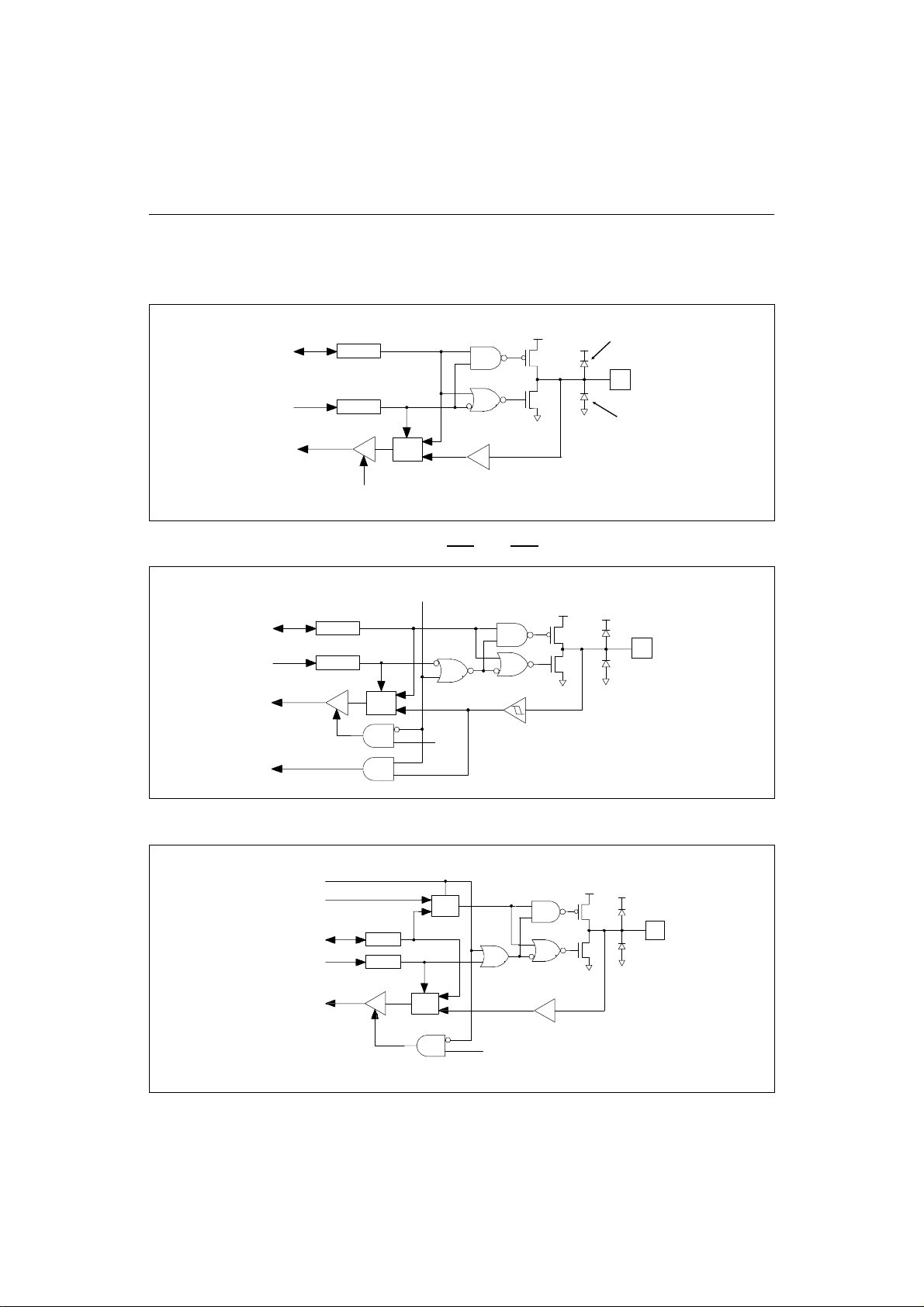
PORT STRUCTURES
R00~R07, R10~R17
V
DATA BUS
DATA BUS
DATA BUS
DATA REG.
DIRECTION REG.
Rd.
MUX
DD
V
SS
PROTECT DIODE
PROTECT DIODE
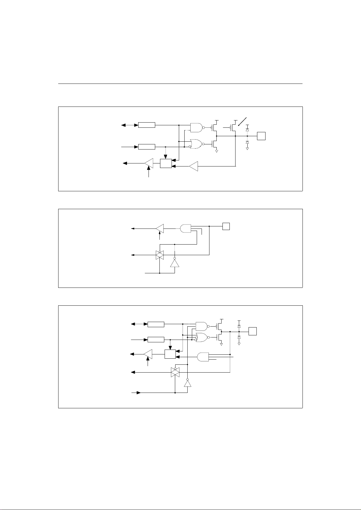
R40/INT0, R41/INT1, R42/INT2, R43/INT3, R44/EC0, R45/EC2
PMR4
DATA REG.
DATA BUS
DATA BUS
DIRECTION REG.
DATA BUS
ALTERNATE FUNCTION
EX) INT0
R46/T1O, R47/T3O, R55/BUZ
Selection (PMR4 or PMR5)
ALTERNATE FUNCTION
EX) T1O
DATA BUS
DATA BUS
DATA BUS
MUX
Rd.
MUX
DATA REG.
DIRECTION REG.
MUX
Rd.
9
GMS81604/08 LG Semicon
R50, R51
DATA REG.
DATA BUS
DIRECTION REG.
DATA BUS
DATA BUS
Rd.
R60/AN0, R61/AN1, R62/AN2, R63/AN3
DATA BUS
TO A/D Converter
Ch. Select
Rd.
MUX
PULL-UP RESISTOR
INPUT MODE: PULL-UP RESISTOR IS ACTIVATED.
OUTPUT MODE: PULL-UP RESISTOR IS DE-ACTIVATED.
Rd.
R64/AN4, R65/AN5, R66/AN6, R67/AN7
DATA BUS
DATA BUS
DATA BUS
TO A/D Converter
Ch. Select
DATA REG.
DIRECTION REG.
Rd.
10
MUX
0: Output
Rd.
1: Reset, Input, AD ch. select
LG Semicon GMS81604/08
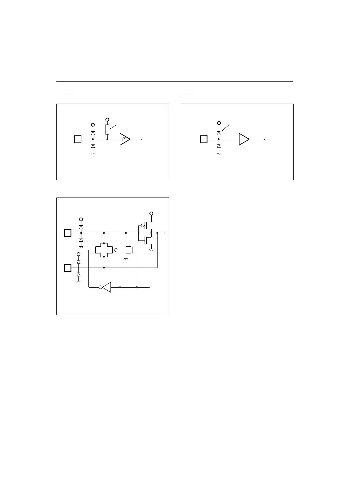
RESET
XIN, X
X
IN
X
OUT
OUT
Pull-up Resister
TEST
OTP: No P-Ch diode
STOP
11
GMS81604/08 LG Semicon
ELECTRICAL CHARACTERISTICS
Absolute Maximum Ratings
Supply Voltage . . . . . . . . . . . . . . . -0.3 to +6.0 V
Storage Temperature . . . . . . . . . . . . -40 to +125 °C
Voltage on any pin with
respect to Ground (VSS) . . . . . . -0.3 to VDD+0.3 V
Maximum current out of VSS pin . . . . . . . . . 150 mA
Maximum current into VDD pin . . . . . . . . . 100 mA
Maximum current sunk by (IOL per I/O Pin) . . . . 20 mA
Maximum output current sourced
by (IOH per I/O Pin) . . . . . . . . . . . . . . . 8 mA
Maximum current (Σ IOL) . . . . . . . . . . . . 120 mA
Maximum current (Σ IOH) . . . . . . . . . . . . . 50 mA
Notice:
Stresses above those listed under "Absolute Maximum Ratings" may cause permanent damage to
the device. This is a stress rating only and functional operation of the device at these of any
other conditions above those indicated in the operational sections of this specification is not implied. Exposure to absolute maximum rating
conditions for extended periods may affect device
reliability.
Recommended Operating Conditions
Parameter Symbol Condition
Supply Voltage V
Operating Frequency f
Operating Temperature T
DD
XIN
OPR
f
= 8 MHz
XIN
f
= 4 MHz
XIN
VDD = 4.5~5.5V
VDD = 2.4~5.5V
Specifications
Min. Max.
4.5
2.4
1
1
5.5
5.5
8
4.2
-20 85
Unit
V
MHz
°C
12
LG Semicon GMS81604/08
DC Characteristics ( 5V )
(VDD = 5.0V± 10%, VSS = 0V, TA = -20 ~ 85 °C, f
Parameter Pin Symbol Test Condition
XIN, RESET,
Input High Voltage
R40~R45
R0,R1,R46,R47
R5,R6
X
RESET,
IN,
Input Low Voltage
R40~R45
R0,R1,R46,R47
R5,R6
Output High Voltage R0,R1,R4,R5,R6 V
Output Low Voltage R0,R1,R4,R5,R6 V
Power Fail Detect
Voltage
Input Leakage
Current
Input Pull-up Current
Power Current
V
DD
RESET, R0, R1,
R4, R5, R6
RESET I
R50, R51 I
Operating mode I
STOP mode I
Hysteresis
* : Data in "Typ" column is at 5 V, 25°C unless otherwise stated. These parameters are for design guidance only and are not tested.
RESET,
R40~R45
= 8 MHz)
XIN
V
V
V
V
V
PFD
I
I
P1
P2
DD
STOP
VT+
~VT-
Specifications
Min. Typ.* Max.
IH1
IH2
IL1
IL2
OH
OL
- 0.8V
- 0.7V
- 0 - 0.2V
- 0 - 0.3V
VDD = 5V
IOH = -2mA
VDD = 5V
IOL = 10mA
VDD -1.0 VDD -0.4 - V
- 0.6 1.0 V
DD
DD
- V
- V
VDD=3~4V 3.0 - 4.0 V
VI = V
IH
IL
DD
VI = 0V -5.0 - 5.0 uA
-5.0 - 5.0 uA
VDD = 5V -180 -120 -30 uA
VDD = 5V -90 -60 -15 uA
f
XIN
f
XIN
=4MHz
=8MHz
4.5
8
VDD = 5V - 2 20 uA
VDD = 5V 0.5 0.8 - V
15
DD
DD
8
DD
DD
Unit
V
V
V
V
mA
A/D Converter Characteristics ( 5V )
(VDD = 5.0V± 10%, V
Parameter Symbol
Analog Input Range V
Non-linearity Error N
Differential Non-linearity Error N
Zero Offset Error N
Full Scale Error N
Accuracy A
AVDD Input Current I
Conversion Time T
Analog power supply Input
Range
* : Data in "Typ" column is at 5 V, 25°C unless otherwise stated. These parameters are for design guidance only and are not tested.
= 5.0V, VSS = 0V, TA = 25 °C)
AIN
AVDD
V
AIN
LE
DIF
OFF
FS
CC
CONV
AVDD
Specifications
Min. Typ.* Max.
V
SS
- 0.7
- 0.1
- 1.5
- 1.0
- 2.0
- V
AVDD
± 1.5
± 0.5
± 2.5
± 1.5
± 3.0
- 0.5 1.0 mA
- - 40 uS
4.5 5.0 5.5
Unit
V
LSB
LSB
LSB
LSB
LSB
V
13
GMS81604/08 LG Semicon
DC Characteristics ( 3V )
(VDD = 3.0V± 10%, VSS = 0V, TA = -20 ~ 85 °C, f
Parameter Pin Symbol Test Condition
XIN, RESET,
Input High Voltage
R40~R45
R0,R1,R46,R47
R5,R6
XIN, RESET,
Input Low Voltage
R40~R45
R0,R1,R46,R47
R5,R6
Output High Voltage R0,R1,R4,R5,R6 V
Output Low Voltage R0,R1,R4,R5,R6 V
Power Fail Detect
Voltage**
Input Leakage
Current
Input Pull-up
Current
Power Current
Hysteresis
* : Data in "Typ" column is at 3 V, 25°C unless otherwise stated. These parameters are for design guidance only and are not tested.
**: Power Fail Detection function is not available on 3V operation.
- - - - - - V
RESET, R0, R1,
R4, R5, R6
RESET I
R50, R51 I
Operating mode I
STOP mode I
RESET,
R40~R45
= 4 MHz)
XIN
V
V
V
V
I
I
P1
P2
DD
STOP
VT+
~VT-
Specifications
Min. Typ.* Max.
IH1
IH2
IL1
IL2
OH
OL
IH
IL
- 0.8V
- 0.7V
- 0 - 0.2V
- 0 - 0.3V
VDD = 3V
IOH = -1mA
VDD = 3V
IOL = 5mA
VI = V
DD
VDD -0.5 VDD -0.3 - V
- 0.5 0.7 V
-3.0 - 3.0 uA
VI = 0V -3.0 - 3.0 uA
DD
DD
- V
- V
VDD = 3V -60 -40 -15 uA
VDD = 3V -30 -20 -7.5 uA
f
=4MHz - 2 5 mA
XIN
VDD = 3V - 1 10 uA
VDD = 3V 0.3 0.6 - V
DD
DD
DD
DD
Unit
V
V
V
V
A/D Converter Characteristics ( 3V )
(VDD = 3.0V± 10%, V
Parameter Symbol
Analog Input Range V
Non-linearity Error N
Differential Non-linearity Error N
Zero Offset Error N
Full Scale Error N
Accuracy A
AVDD Input Current I
Conversion Time T
Analog power supply Input
Range
* : Data in "Typ" column is at 3 V, 25°C unless otherwise stated. These parameters are for design guidance only and are not tested.
= 3.0V, VSS = 0V, TA = 25 °C)
AIN
AVDD
V
AIN
LE
DIF
OFF
FS
CC
CONV
AVDD
Specifications
Min. Typ.* Max.
V
SS
- 0.2
- 0.1
- 2.0
- 1.0
- 2.0
- V
AVDD
± 1.0
± 0.5
± 2.5
± 1.5
± 3.0
- 0.3 0.5 mA
- - 40 uS
2.7 3.0 3.3
Unit
V
LSB
LSB
LSB
LSB
LSB
V
14
LG Semicon GMS81604/08
AC Characteristics
(VDD = 2.7~5.5V, VSS = 0V, TA = -20 ~ 85 °C)
Parameter Pin Symbol
Main clock frequency X
Oscillation stabilization Time XIN, X
External Clock Pulse Width X
External Clock Transition Time X
IN
OUT
IN
IN
Interrupt Pulse Width INT0, INT1, INT2, INT3 t
RESET Input Low Width RESET t
Event Counter Input Pulse
Width
EC0, EC2 t
Event Counter Transition Time EC0, EC2 t
*: t
is 2/f
XIN
.
SYS
t
RCP
REC
f
t
t
CPW
RST
ECW
XIN
ST
, t
IW
, t
FCP
FEC
Specifications
Min. Typ. Max.
1 - 8 MHz
20 - - ms
80 - - ns
- - 20 ns
2 - - t
8 - - t
2 - - t
- - 20 ns
Unit
SYS
SYS
SYS
*
*
*
Timing Chart
t
1 / f
XIN
X
IN
CPWtCPW
0.9V
0.1V
DD
DD
INT0, INT1
INT2, INT3
RESET
EC0, EC2
0.8V
t
RCPtFCP
t
IW
DD
0.8V
t
REC
0.2V
DD
t
RST
t
ECW
DD
t
0.2V
FEC
DD
0.2V
t
ECW
t
IW
DD
15
GMS81604/08 LG Semicon
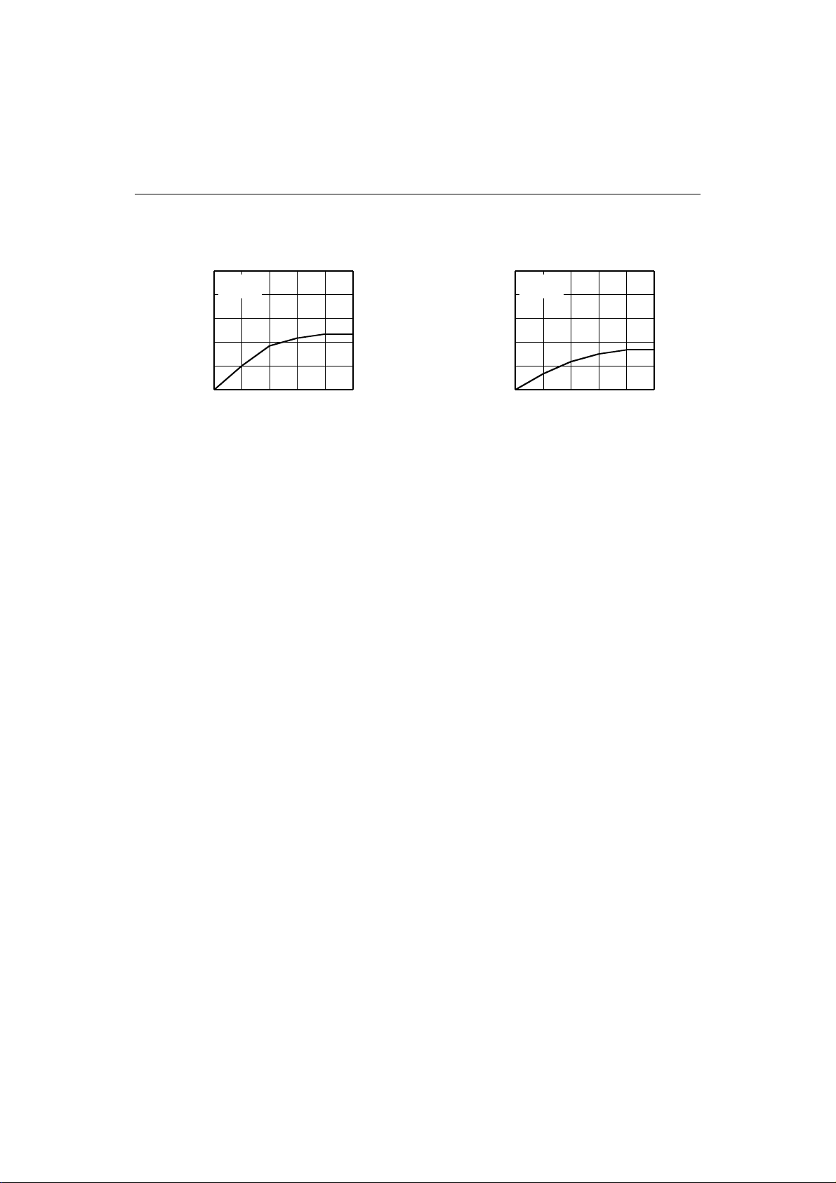
TYPICAL CHARACTERISTICS
These parameters are for design guidance only and are not tested.
VDD=5V
I
DD
(mA)
I
OL
(mA)
IDD - V
DD
TA=25°C
8
6
4
2
IOL - V
VDD=5.0V
24
18
12
6
0
f
XIN
f
= 4MHz
XIN
2 3 4 506 (V)
OL
TA=25°C
1 2 3 4
= 8MHz
I
STOP
I
STOP
(uA)
TA=25°C
8
6
4
2
V
DD
I
(mA)
V
OL
(V)
2 3 4 506 (V)
IOH - V
OH
24
18
12
6
0
OH
VDD=5.0V
TA=25°C
1 2 3 4
VDD-V
(V)
V
DD
OH
16
Operating area
f
XIN
(MHz)
TA = -20~80°C
8
6
4
2
0
1
2 3 4 5
V
DD
(V)
LG Semicon GMS81604/08
VDD=3.0V
I
OL
(mA)
20
IOL - V
VDD=3.0V
TA=25°C
OL
I
OH
(mA)
-8
IOH - V
VDD=3.0V
TA=25°C
OH
15
10
5
0
0.5 1.0 1.5 2.0
-6
-4
-2
VDD-V
V
OL
(V)
0
0.5 1.0 1.5 2.0
OH
(V)
17
GMS81604/08 LG Semicon
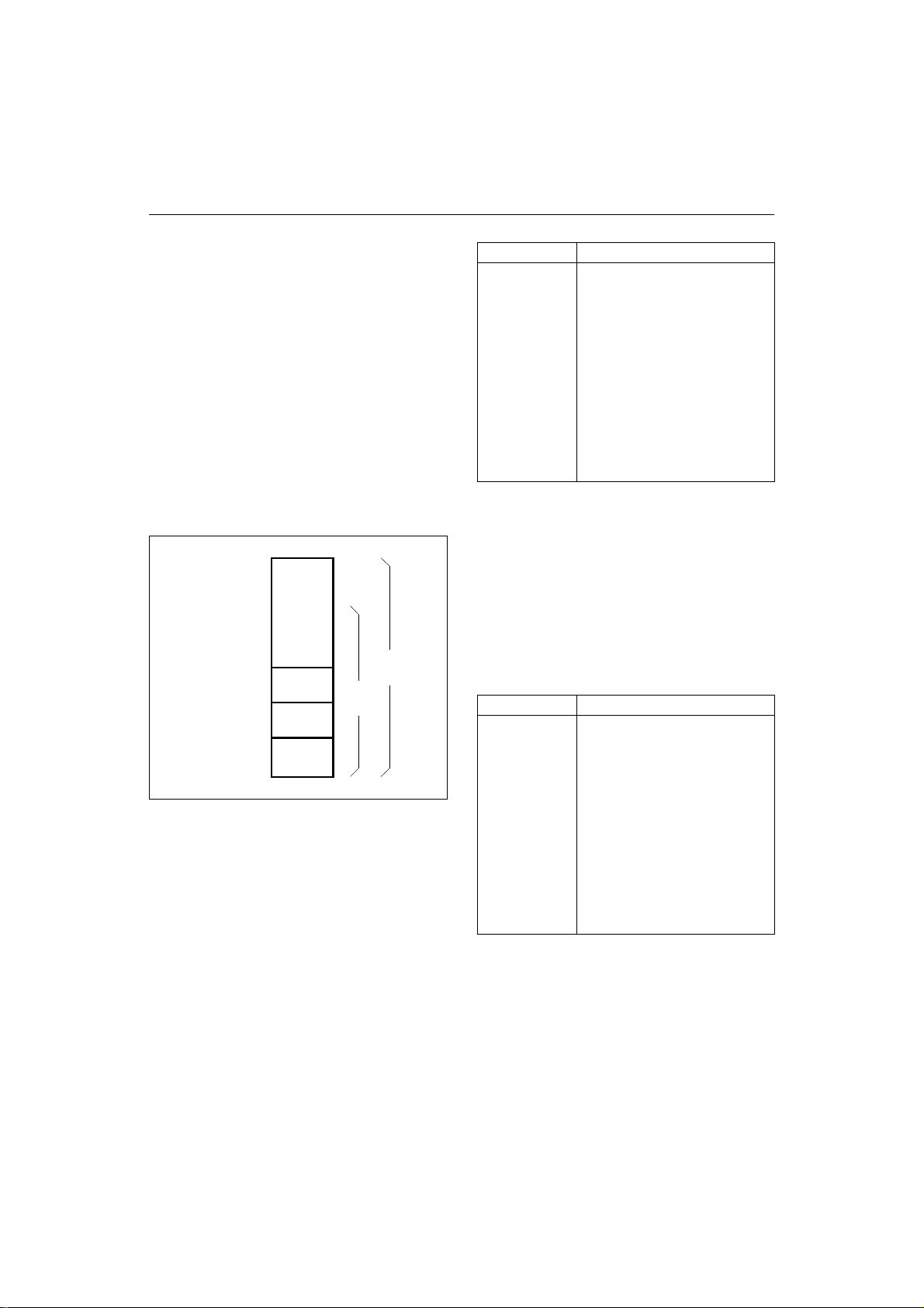
MEMORY ORGANIZATION
The GMS81604 has separate address spaces for Program and Data Memory. Program memory can only be
read, not written to. It can be up to 4K (8K for
GMS81608) bytes of Program Memory. Data memory can be read and written to up to 256 bytes including
the stack area.
Registers
This device has six registers that are the Program
Counter (PC), a Accumulator (A), two Index registers
(X,Y), the Stack Pointer (SP) and the Program Status
Word (PSW). The Program Counter consists of 16-bit
register.
A
X
Y
SP
PCH PCL
PSW
ACCUMULATOR
X REGISTER
Y REGISTER
STACK POINTER
PROGRAM COUNTER
PROGRAM STATUS
WORD
Figure 3. Configuration of Registers
Accumulator: The accumulator is the 8-bit general
purpose register, used for data operation such as transfer, temporary saving and conditional judgment, etc.
The accumulator can be used as a 16-bit register with
Y register as shown below.
Y
Y A
A
TWO 8-BIT REGISTERS ONE "YA" 16-BIT REGISTER
Figure 4. Configuration of YA 16-bit register
X register, Y register: In the addressing modes which
use these index registers, the register contents are
added to the specified address and this becomes the
actual address. These modes are extremely effective
for referencing subroutine tables and memory tables.
The index registers also have increment, decrement,
compare and data transfer functions and they can be
used as simple accumulators.
Stack Pointer: The stack pointer is an 8-bit register
used for occurrence interrupts and calling out subroutines. The stack can be located at any position within
100H to 13FH of the internal data memory. Data store
and restore sequence to(from) stack area is shown in
Figure 0.
Caution:
The stack pointer must be initialized by software
because its value is undefined after reset.
Ex) LDX #03FH
TXSP ; SP ← 3F
Stack Address (100H~13FH)
15 8 7 0
1 SP
Hardware fixed.
H
Figure 5. Stack Pointer
Program Counter: The program counter is a 16-bit
wide which consists of two 8-bit registers, PCH, PCL.
This counter indicates the address of the next instruction to be executed. In reset state, the program counter
has reset routine address (PCH: FFH, PCL: FEH). .
Program Status Word : The Program Status Word
(PSW) contains several status bits that reflect the current state of the CPU. The PSW shown in Figure 6. It
contains the Negative flag, the Overflow flag, the
Direct page flag, the Break flag, the Half Carry (for
BCD operations), the Interrupt enable flag, the Zero
flag and the Carry bit.
[Carry flag C]
This flag stores any carry or borrow from the ALU of
CPU after an arithmetic operation and is also changed
by the Shift instruction or rotate instruction.
[Zero flag Z]
This flag is set when the result of an arithmetic operation or data transfer is "0" and is cleared by any other
result.
[Interrupt disable flag I] This flag enables/disables all
interrupts except interrupt caused by Reset or software
18
LG Semicon GMS81604/08
MSB LSB
PSW
NEGATIVE FLAG
OVERFLOW FLAG
N
V G B H I Z C
RESET VALUE: 00H
CARRY FLAG RECEIVES
CARRY OUT
ZERO FLAG
G FLAG TO SELECT DIRECT PAGE
BRK FLAG
Figure 6. PSW (Program Status Word) Register
BRK instruction. All interrupts are disabled when
cleared to "0". This flag immediately becomes "0"
when an interrupt is served. It is set by the EI instruction, cleared by the DI instruction.
[Half carry flag H]
After operation, set when there is a carry from bit 3 of
ALU or there is not a borrow from bit 4 of ALU. This
bit can not be set or cleared except CLRV instruction,
clearing with Overflow flag (V).
[Break flag B]
This flag set by software BRK instruction to distinguish BRK from TCALL instruction which as the
same vector address.
[Direct page flag G]
This flag assign direct page for direct addressing mode.
In the direct addressing mode, addressing area is
INTERRUPT ENABLE
FLAG
HALF CARRY FLAG RECEIVES
CARRY OUT FROM BIT 1 OF
ADDITION OPERANDS
within zero page 00H to FFH when this flag is "0". If it
is set to "1", addressing area is 100H to 1FFH.
It is set by SETG instruction, and cleared by CLRG.
[Overflow flag V]
This flag is set to "1" when an overflow occurs in the
result of an arithmetic operation involving signs. An
overflow occurs when the result of an addition or
subtraction exceeds +127(7FH) or -128(80H).
The CLRV instruction clears the overflow flag. There
is no set instruction. When the BIT instruction is
executed, for other than the above, bit 6 of memory is
copy to this flag.
[Negative flag N]
This flag is set to match the sign bit (bit 7) status of the
result of a data or arithmetic operation. When the BIT
instruction is executed, bit 7 of memory is copy to this
flag.
1) INTERRUPT
M(SP) ← (PCH)
SP ← SP - 1
M(SP) ← (PCL)
SP ← SP - 1
M(SP) ← (PSW)
SP ← SP - 1 (PCH) ← M(SP)
2) RETI
SP ← SP + 1
(PSW) ← M(SP)
SP ← SP + 1
(PCL) ← M(SP)
SP ← SP + 1
3) CALL
M(SP) ← (PCH)
SP ← SP - 1
M(SP) ← (PCL)
SP ← SP - 1
Figure 7. Stack Operation
4) RET
SP ← SP + 1
(PCL) ← M(SP)
SP ← SP + 1
(PCH) ← M(SP)
5) PUSH A (X,Y,PSW)
M(SP) ← ACC.
SP ← SP - 1
6) POP A (X,Y,PSW)
SP ← SP + 1
M(SP) ← (PCH)
19
GMS81604/08 LG Semicon
Program Memory
A 16-bit program counter is capable of addressing up
to 64K bytes, but this devices have 4K bytes (8K for
GMS81608) program memory space only the physically implemented. Accessing a location above FFFF
will cause a wrap-around to 0000H.
Figure 8, shows a map of the upper part of the Program
Memory. After reset, the CPU begins execution from
reset vector which is stored in address FFFEH, FFFFH.
As shown in Figure 8, each area is assigned a fixed
location in Program Memory. Program Memory area
contains the user program, Page Call (PCALL) area
contains subroutine program, to reduce program byte
length because of using by 2 bytes PCALL instead of
3 bytes CALL instruction. If it is frequently called,
more useful to save program byte length.
E000H
F000H
PROGRAM
MEMORY
FEFFH
FF00H
FFBFH
FFC0H
FFDFH
FFE0H
FFFFH
PCALL
AREA
TCALL
AREA
INTERRUPT
VECTOR
AREA
GMS81608
GMS81604
Figure 8. Program Memory
Table Call (TCALL) causes the CPU to jump to each
TCALL address, where it commences execution of the
service routine. The Table Call service locations are
spaced at 2-byte interval : FFC0H for TCALL15,
FFC2H for TCALL14, etc.
Address TCALL Name
FFC0H
FFC2H
FFC4H
H
FFC6H
FFC8H
FFCAH
FFCCH
FFCEH
FFD0H
FFD2H
FFD4H
FFD6H
FFD8H
FFDAH
FFDCH
FFDEH
1) The BRK software interrupt is using same address with
TCALL0.
TCALL15
TCALL14
TCALL13
TCALL12
TCALL11
TCALL10
TCALL9
TCALL8
TCALL7
TCALL6
TCALL5
TCALL4
TCALL3
TCALL2
TCALL1
TCALL0/ BRK
1)
The interrupt causes the CPU to jump to specific
location, where it commences execution of the service
routine. The External interrupt 0, for example, is assigned to location FFFAH. The interrupt service locations are spaced at 2-byte interval : FFF8H for External
Interrupt 1, FFFAH for External Interrupt 0, etc.
Any area from FF00H to FFFFH, if it not going to be
used, its service location is available as general purpose Program Memory.
Address Vector Name
FFE0H
FFE2H
FFE4H
FFE6H
FFE8H
FFEAH
FFECH
FFEEH
FFF0H
FFF2H
FFF4H
FFF6H
FFF8H
FFFAH
FFFCH
FFFEH
-
-
Basic Interval Timer
Watch Dog Timer
Analog to Digital Converter
Timer/ Counter 3
Timer/ Counter 2
Timer/ Counter 1
Timer/ Counter 0
External Interrupt 3
External Interrupt 2
External Interrupt 1
External Interrupt 0
RESET
20
 Loading...