

HEI GMS81516, GMS81508 Datasheet

GMS81508A
GMS81516A
USER’S MANUAL
Revision History
Rev 2.2 (Dec. 1998)
Add the package dimension for 64LQFP on page 3-1, 4-1.
Rev 2.1 (Nov. 1998)
Operating Temperature, -10~75°C is extended to -20~85°C.
Add the unused port guidance on page 55.
Correct errata for opcode of “EOR [dp+X], EOR [dp]+Y, EOR {X}” in “Instruction Set”.
Add the OTP device programming guidance, recommend using “Intelligent Mode”.
Add the chapter for OTP programming manual as an appendix.
Rev 2.0 (Sep. 1997)

- CONTENTS -
1. OVERVIEW...........................................................................................................................................1
1.1. FEATURES..........................................................................................................................................1
1.2. BLOCK DIAGRAM..............................................................................................................................2
1.3. PIN ASSIGNMENT ..............................................................................................................................3
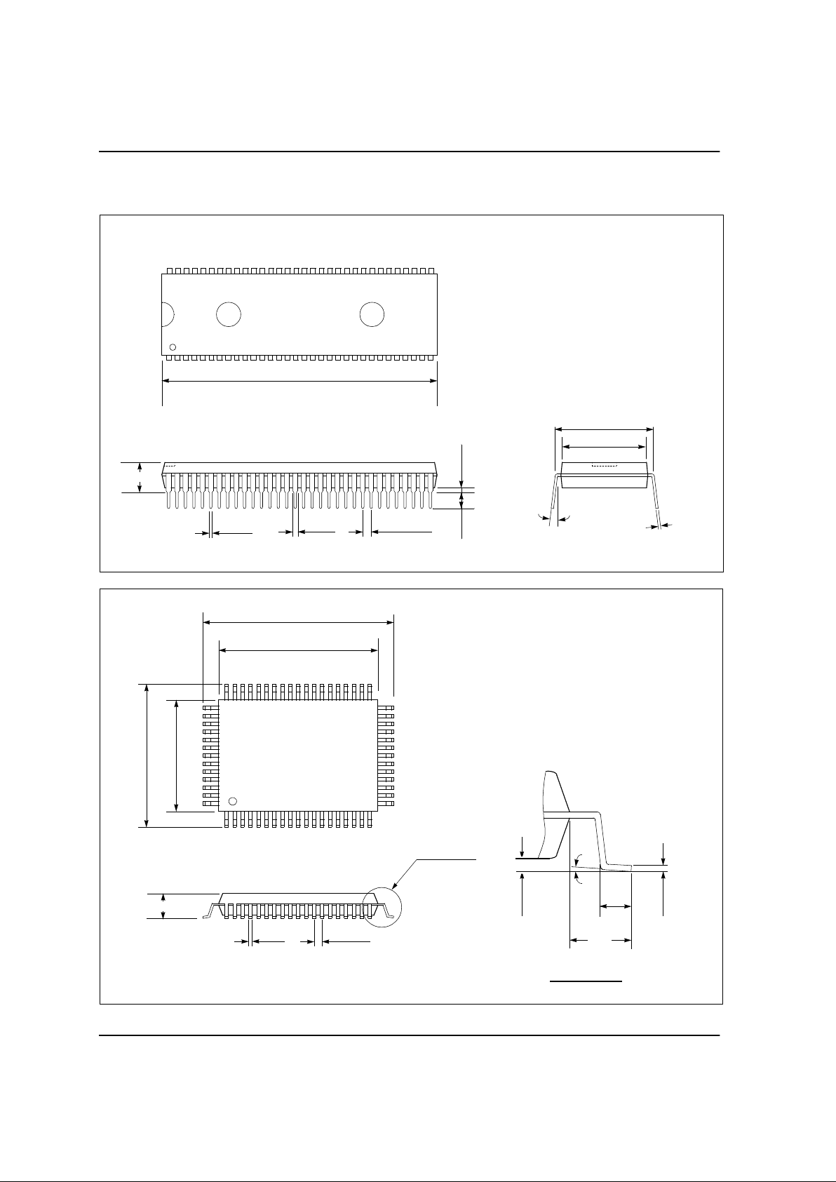
1.4. PACKAGE DIMENSION .....................................................................................................................4
1.5. PIN DESCRIPTION..............................................................................................................................5
2. FUNCTIONS..........................................................................................................................................7
2.1. REGISTERS.........................................................................................................................................7
2.1.1. A - Register....................................................................................................................................8
2.1.2. X- Register.....................................................................................................................................8
2.1.3. Y- Register.....................................................................................................................................8
2.1.4. Stack Pointer .................................................................................................................................8
2.1.5. Program Counter.........................................................................................................................10
2.1.6. Program Status Word...................................................................................................................10
2.2. MEMORY SPACE..............................................................................................................................12
2.2.1. RAM area....................................................................................................................................12
2.2.2. Peripheral Register area..............................................................................................................12
2.2.3. Progr a m ROM area.....................................................................................................................12
2.2.4. Peripheral Register List ...............................................................................................................14
2.3. CLOCK GENERATION CIRCUIT.....................................................................................................16
2.3.1. Oscillation Circuit .......................................................................................................................16
2.3.2. Prescaler.....................................................................................................................................17
2.4. BASIC INTERVAL TIMER................................................................................................................18
2.4.1. Control of Basic Interval Timer....................................................................................................18
2.5. WATCH DOG TIMER........................................................................................................................ 19
2.5.1. Control of Watch Dog Timer........................................................................................................19
2.5.2. The output of WDT signal.............................................................................................................20
2.6. TIMER................................................................................................................................................21
2.6.1. Control of Timer .......................................................................................................................... 23
2.6.2. Interval Timer..............................................................................................................................24
2.6.3. Event Counter..............................................................................................................................24
2.6.4. Pulse Output................................................................................................................................ 24
2.6.5. Input Capture...............................................................................................................................24
2.7. EX TERNA L INTERRUPT..................................................................................................................26
2.8. A/D CONVERTER ............................................................................................................................. 27
2.8.1. Control of A/D Converter.............................................................................................................27
2.9. SERIAL I/O........................................................................................................................................29
2.9.1. Data Transmission/Receiving Timing...........................................................................................31
2.9.2. The Serial I/O operation by Srdy pin ............................................................................................ 31
2.9.3. The method of Serial I/O..............................................................................................................32
2.9.4. The Method to Test Correct Transmission with S/W......................................................................32
2.10. PWM ................................................................................................................................................33
2.10.1. Controls of PWM ....................................................................................................................... 33
2.11. BUZZER DRIVER............................................................................................................................35
2.11.1. Buzzer Driver Operation............................................................................................................36
2.12. INTERRUPTS...................................................................................................................................37
2.12.1. Interrupt Circuit Configuration and Kinds ..................................................................................37
2.12.2. Interrupt Control........................................................................................................................38
2.12.3. Interrupt Priority ..................................................................................................... ..................39

2.12.4. Interrupt Sequence.....................................................................................................................40
2.12.5. Software Interrupt ..................................................................................................................... 41
2.12.6. Multiple Interrupt...................................................................................................................... 42
2.13. STANDBY FUNCTION...................................................................................................................44
2.13.1. STOP Mode............................................................................................................................... 45
2.13.2. STOP Mode Release.................................................................................................................. 45
2.14. RESET FUNCTION......................................................................................................................... 47
3. I/O PORTS...........................................................................................................................................48
3.1. R0 PORT............................................................................................................................................ 48
3.2. R1 PORT............................................................................................................................................ 49
3.3. R2 PORT............................................................................................................................................ 50
3.4. R3 PORT............................................................................................................................................ 51
3.5. R4 PORT............................................................................................................................................ 52
3.6. R5 PORT............................................................................................................................................ 53
3.7. R6
PORT............................................................................................................................................ 54
3.8. TERMINA L TYPES........................................................................................................................... 56
4. ELECTRICAL CHARACTERISTICS............................................................................................... 60
4.1. ABOULUTE MAXIMUM RATINGS.................................................................................................60
4.2. RECOMMENDED OPERATING CONDITIONS............................................................................... 60
4.3. A/D CONVERTER CHARACTERISTICS .........................................................................................60
4.4. DC CHARACTERISTICS........................................................................................................ .......... 61
4.5. AC CHARACTERISTICS........................................................................................................ .......... 62
4.5.1. Input Conditions.......................................................................................................................... 62
4.5.2. Serial Transfer............................................................................................................................63
4.5.3. Microprocessor Mode I/O Timing................................................................................................64
4.5.4. Bus Holding Timing.....................................................................................................................65
5. INSTRUCTION SET........................................................................................................................... 66
GMS81508/16
1
1. OVERVIEW
GMS81508/16 is a singl e c hip mi c r oc om puter designed CMOS technology. The use of CMOS
process enables ext r em ely low power consumption.
This devic e using the G8MC Cor e incl udes several peripheral functions such as Timer, A/D
Converter, Programmable Buzzer Driver, Serial I/ O, P ulse Width Modulation Function, et c.
ROM,RAM,I/O are plac ed on the same memory map in addition to simple instruc tion set.
1.1. FEATURES
GMS81508 GMS81516
ROM(Bytes)
8K 16K
RAM(Bytes)
448 bytes(includes stack area)
Execution Time
0.5us (@Xin=8MHz )
Basic Interval Timer
8bit ✕ 1ch.
Watch Dog Timer
6bit ✕ 1ch.
Timer
8bit✕4ch.(or 16bit ✕ 2ch.)
ADC
8bit ✕ 8ch.
PWM
8bit ✕ 2ch.
Serial I/O
8bit ✕ 1ch.
External Interrupt
4ch.
Buzzer Driver
Programmable B uzzer Driving Port
I/O Port
4 - Input only
52 - Input/Output
Power Save Mode
STOP Mode
Operating Volt age
4.5 ∼ 5.5V ( @ Xin=8MHz )
Operating Frequ ency
1 ∼ 8MHz
Package
64SDIP, 64QFP
OTP
GMS81516T
Application
Home Appliances, LED Applications
HYUNDAI MicroElectronics
2
1.2. BLOCK DIAGRAM
A/D
CONVERTER
PWM
BUZZER
W.D.T
S.I.C
TIMER
INTERRUPT
CLOCK GEN.
/
SYSTEM
CONTROL
G8MC
CORE
RAM
(448 BYTE)
ROM
(8/16K BYTE)
PRESCALER
/
B.I.T
R6
PORT
R5
PORT
R4
PORT
R3
PORT
R2
PORT
R1
PORT
R0
PORT
AVref AVss
R60~R67
(AN0~AN7)
R57/PWM1
R55/BUZ
R56/PWM0
R54/WDTO
R53/Srdy
R52/Sclk
R51/Sout
R50/Sin
R47/T3 O
R46/T1 O
R45/EC2
R44/EC0
R43/INT3
R42/INT2
R41/INT1
R40/INT0
MP
RESET
Xin
Xout
Vdd Vss
R60
:
R63
R64
:
R67
R50
:
R57
R40
:
R47
R30
:
R37
R20
:
R27
R10
:
R17
R00
:
R07
GMS81508/16
3
1.3. PIN ASSIGNMENT
G
M
S
8
1
5
0
8
/
1
6
R30/ RD
R31/ Wt
R32/ R/W
R33/ C
R34/ SYNC
R35/ BRK
R36/ BRQ
R37/ HALT
R00/ D0
R01/ D1
R02/ D2
R03/ D3
R04/ D4
R05/ D5
R06/ D6
R07/ D7
R10/ A0
R11/ A1
R12/ A2
R13/ A3
R14/ A4
R15/ A5
R16/ A6
R17/ A7
R20/ A8
R21/ A9
R22/ A10
R23/ A11
R24/ A12
R25/ A13
R26/ A14
R27/ A15
Vdd
MP
AVss
AVref
R67/AN7
R66/AN6
R65/AN5
R64/AN4
R63/AN3
R62/AN2
R61/AN1
R60/AN0
R57/PWM1
R56/PWM0
R55/BUZ
R54/WDTO
R53/Srdy
R52/Sclk
R51/Sout
R50/Sin
R47/T3O
R46/T1O
R45/EC2
R44/EC0
R43/INT3
R42/INT2
R41/INT1
R40/INT0
RESET
Xin
Xout
Vss
1
2
3
4
5
6
7
8
9
10
11
12
13
14
15
16
17
18
19
20
21
22
23
24
25
26
27
28
29
30
31
32
64
63
62
61
60
59
58
57
56
55
54
53
52
51
50
49
48
47
46
45
44
43
42
41
40
39
38
37
36
35
34
33
MP MODE
64 SDIP
GMS81508/16
R65/AN5
R64/AN4
R63/AN3
R62/AN2
R61/AN1
R60/AN0
R57/PWM1
R56/PWM0
R55/BUZ
R54/WDTO
R53/Srdy
R52/Sclk
R51/Sout
R50/Sin
R47/T3O
R46/T1O
R45/EC2
R44/EC0
R43/INT3
21
31 2 4 5 6 7 8 9 10 11 12 13 14 15 16 17 18 19
22
23
24
25
26
27
28
29
30
31
32
20
4951 50 48 47 46 45 44 43 42 41 40 39 38 37 36 35 34 33
63
62
61
60
59
58
57
56
55
54
53
52
64
R37/HALT
R00/D0
R01/D1
R02/D2
R03/D3
R04/D4
R05/D5
R06/D6
R07/D7
R10/A0
R11/A1
R12/A2
R13/A3
R14/A4
R15/A5
R16/A6
R17/A7
R20/A8
R21/A9
R22/A10
R23/A11
R24/A12
R25/A13
R26/A14
R17/A15
Vss
Xout
Xin
RESET
R40/INT0
R41/INT1
R42/INT2
R36 BRQ
R35 BAK
R34 SYNC
R33 C
R32 R/W
R31 Wt
R30 Rd
Vdd
MP
AVss
AVref
R67/AN7
R66/AN6
64 QFP
HYUNDAI MicroElectronics
R20
R21
R22
R23
R24
R25
R26
R27
VSS
XOUT
XIN
RESET
R40/INT0
R41/INT1
R42/INT2
R43/INT3
R00
R01
R02
R03
R04
R05
R06
R07
R10
R11
R12
R13
R14
R15
R16
R17
R63/AN3
R62/AN2
R61/AN1
R60/AN0
R57/PWM1
R56/PWM0
R55/BUZ
R54/WDTO
R53/SRDY
R52/SCLK
R51/SOUT
R50/SIN
R47/T3O
R46/T1O
R45/EC2
R44/EC0
123456789
10111213141516
R37
R36
R35
R34
R33
R32
R31
R30
VDD
MP
AVSS
AVREF
R67/AN7
R66/AN6
R65/AN5
R64/AN4
484746454443424140393837363534
33
32
31
30
29
28
27
26
25
24
23
22
21
20
19
18
17
49
50
51
52
53
54
55
56
57
58
59
60
61
62
63
64
GMS81508/16
64LQFP
3-1
HYUNDAI MicroElectronics
4
1.4 PACKAGE DIMENSION
UNIT: INCH
2.280
2.260
0.205 max.
0.022
0.016
0.050
0.030
0.070 BSC
0.140
0.120
min. 0.015
0.680
0.660
0.750 BSC
0-15
°
0.012
0.008
64SDIP
20.10
19.90
24.15
23.65
18.15
17.65
14.10
13.90
3.18 max.
0.50
0.35
1.00 BSC
SEE DETAIL "A"
1.03
0.73
0-7
°
0.36
0.10
0.23
0.13
1.95
REF
DETAIL "A"
UNIT: MM
64QFP
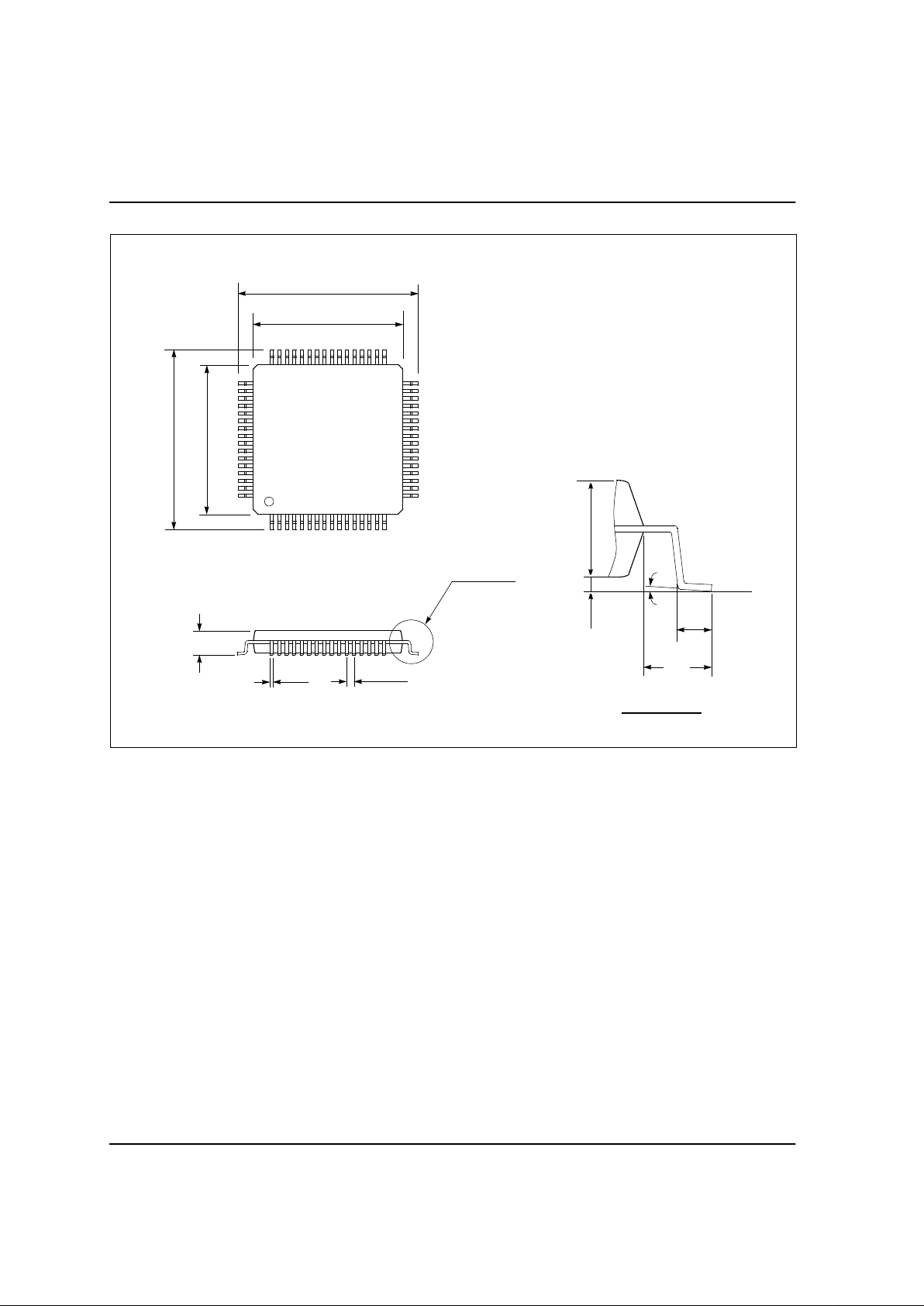
HYUNDAI MicroElectronics
1.60 max.
SEE DETAIL "A"
0.75
0.45
0-7
°
0.15
0.05
1.00
REF
DETAIL "A"
UNIT: MM
10.00 BSC
12.00 BSC
12.00 BSC
10.00 BSC
0.38
0.22
0.50 BSC
1.45
1.35
64LQFP
4-1
GMS81508/16
5
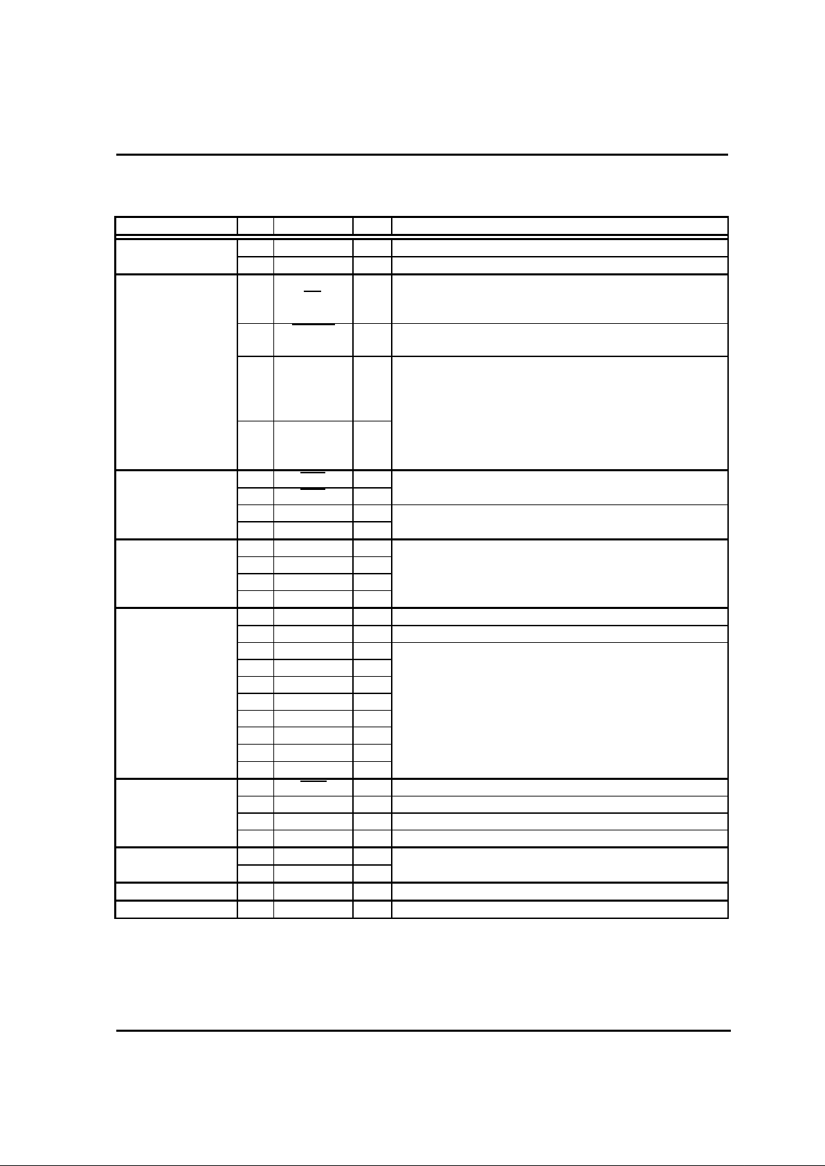
1.5. PIN DESCRIPTION
Classification No. Symbol I/O Descriptions
Power 1 Vdd I Power Supply Input Pi n( 4.5~5.5V)
32 Vss I Ground(0V)
2MP
I Controls Micropr oc ess Mode of the Chip
At "H" input : Single Chip M ode
At "L" input : Microprocess Mode
System Controlor29 RESET I In the state of "L" level, system enter to the reset
state.
Clock
30 Xin
I This chip has an inter nal cl oc k gener ating circuit. To
control gener ating frequency, an external c er ami c or
a quartz crystal oscillator is connected between Xin
and Xout pins.
31 Xout I If external clock is used, the clock source should be
connected to the Xi n pi n and the Xout pin should be
left open.
24 EC0 I Event Counter Source Cloc k Input Pin
Timer 23 EC2 I
22 T1O O Timer Counter Overflow Output Pin
21 T3O O
28 INT0 I
Ext. Interr upt 27 INT 1 I External Inter r upt Request Signal Input Pin
26 INT2 I
25 INT3 I
4 AVref I Referenc e Voltage Input Pin for A/D Converter
3 AVss I Ground Level Input Pin for A/D Converter
12 AN0 I
11 AN1 I
A/D Converter 10 AN2 I
9 AN3 I Analog Voltage Input Pin for A/ D Conv erter
8AN4 I
7AN5 I
6AN6 I
5AN7 I
17 Srdy I/O Receive Enable Output Pin
Serial I/O 18 Sclk I/O Serial Clock Output Pin
19 Sout O Serial Dat a Output Pin
20 Sin I Serial Data Input Pin
P.W.M 14 PWM0 O PWM Pulse Output Pin
13 PWM1 O
Buzzer 15 BUZ O Buzzer Driving Frequency Out put Pin
W.D.T 16 WDTO O Watch dog Timer Overflow Output Pin

HYUNDAI MicroElectronics
6
Classification No. Symbol I/O Description
49
:
56
R00
:
R07
I/O
R0 Port
( Can be determined I/O by R0DD )
In MP mode, This port functions as 8-bit data bus for
the CPU. (D0~D7)
41
:
48
R10
:
R17
I/O
R1 Port
( Can be determined I/O by R1DD )
In MP mode, This functions as 8-bit lower address
output pins. (A0~A7)
33
:
40
R20
:
R27
I/O
R2 Port
( Can be determined I/O by R2DD )
In MP mode, This functions as 8-bit higher address
output pins.(A8~A15)
I/O Port 57
:
64
R30
:
R37
I/O
R3 Port
( Can be determined I/O by R3DD )
In MP mode, This port functions as 8-bit control bus
for the CPU.
28
:
21
R40
:
R47
I/O
R4 Port
( Can be determined I/O by R4DD )
20
:
13
R50
:
R57
I/O
R5 Port
( Can be determined I/O by R5DD )
12
:
9
R60
:
R63
I
R6 Port
Input Only
8
:
5
R64
:
R65
I/O R6 Port
( Can be determined I/O by R6DD )
GMS81508/16
7
2. FUNCTIONS
2.1. REGISTERS
6 registers are built-in the CPU of G8MC. Accumulator(A) , I ndex regi st er X, Y, Stac k P ointer (SP)
and Program Status Word(PSW) consists of 8-bit registers. P r ogr am Counter(PC) consists of 16bit registers. The contents of these registers are undefined after RESET.
P
rogram Counter
15 8
PCH
7 0
PCL
A
- Register
7 0
A
15 8
Y
( YA 16bit Accumulator )
7 0
A
X
- Register
7 0
X
Y
- Register
7 0
Y
P
rogram Status Word
7 0
PSW
S
tack Pointer
7 0
SP
C
arry Flag
Z CH IG BN V
Z
ero Flag
I
nterrupt Enable Flag
H
alf Carry Flag
B
reak Flag
G
( Direct Page ) Flag
O
verflow Flag
N
egative Flag

HYUNDAI MicroElectronics
8
2.1.1. A - Register
The accumulator is the 8-bit general purpose register. This is used register for data oper ation, data
transfer, temporary saves and conditional judgment.
Accumulator can be used as a 16-bit r egister with Y r egister and has a lower 8- bit data.
In case of multiplication instruction(MUL), it wor k s as a multiplier. After exec ution of MUL
instruction, Accumulator has lower 8- bit data of the results(16-bit).
In case of division instruction(DIV), it has the lower 8- bit of dividend (16-bit)
2.1.2. X- Register
In index addressing mode, this register is executed as a 8-bit index register within dir ec t page(RA M
area). also, In indirec t addressing mode, it is destination address register.
This register can be used as a increment, dec r ement, comparison, and data transfer function.
In case of division instruction(DIV), it work s as a divisor .
2.1.3. Y- Register
In index addressing mode, this register is executed as a index register.
In case of 16-bit operation instruction, this register has upper 8- bit of YA (16-bit accumulator) .
In case of multiplication instruction(MUL), this register is exec uted as a multiplicand register. After
multiplication operation, it has the upper 8-bit of the r esult.
In case of division instruction, it is executed as a dividend(upper 8- bit). After division operation, it
has quotient.
This register can be used as a loop counter of conditional branch command. (e.g. DBNE Y , rel)
2.1.4. Stack Pointer
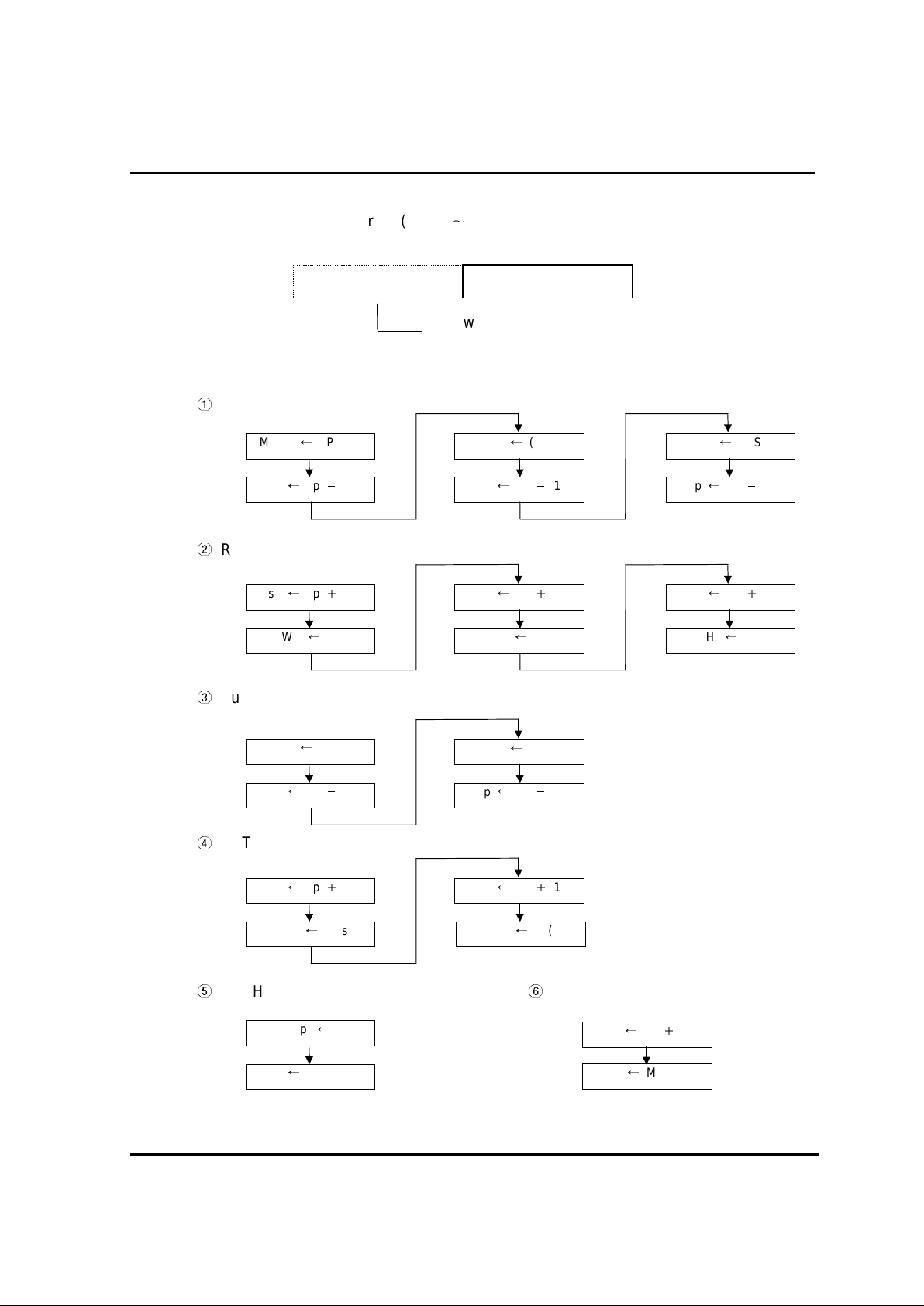
The stack pointer(SP) is an 8-bit register used during subroutine calling and interrupts.
When branching out from an on-going routine to subroutine or interrupt routine, it is necessary to
remember the return address. normally , internal RA M is used for stor ing the retur n addr ess and
this area is called stack area. SP is pointer to show wher e the stac k data ar e stor ed within the
stack area.
The stack area is located in 1-Page of inter nal RAM. SP must be initialized by S/W because the
contents of SP is undefined after RESET.
ex) LDX #0FEH ;0FEH -> X register
TXSP ;X -> SP
caution) You can't use !01FFH as stack. If you use this area, mal-function would be
occurred.
GMS81508/16
9
The bellows shows data store and restore s equenc e to/from stack ar ea.
Interrupt
RETI
Subroutine CALL
RET
PUSH A ( X, Y, PSW )
POP A ( X, Y, PSW )
M (sp) ( PCH )
sp sp 1
M (sp) ( PCL )
sp sp 1
M (sp) A
M (sp) ( PCH )
sp sp 1
M (sp) ( PCL )
sp sp 1
M (sp) ( PSW )
sp sp 1
sp sp 1
sp sp 1
( PCL ) M (sp)
sp sp 1
( PCH) M (sp)
sp sp 1
A M (sp)
( PSW ) M (sp)
sp sp 1
( PCL ) M (sp)
sp sp 1
( PCH) M (sp)
sp sp 1
15 8
Stack Address ( 0100
H
01FF
H
)
01
H
7 0
SP
Hardware fixed

HYUNDAI MicroElectronics
10
2.1.5. Program Counter
The program counter ( P C) is a 16- bit counter whic h c onsists of 8-bit register PCH and PCL. The
addressing space is 64K bytes.
This counter indicates the address of the next instruction to be executed.
In reset state, the program c ounter (P C) has r eset routine address in address FFFFH and FFFEH .
2.1.6. Program Status Word
PSW is an 8-bit register which is composed of flags to maintain the condition of the processor
immediately after an operation.
After RESET, The contents of P SW is set to "00H".
PSW
Carry Flag ( C )
After an operation, it is set to "1" when there is a car r y fr om bit7 of ALU or not a borrow.
SETC,CLRC instructions allow direct access for setting and r esetting.
it can be used as a 1-bit accumulator.
It is a branch condition flag of BCS, BCC instruc tions.
Zero Flag ( Z )
After an operation including 16-bit operation, it is set to "1" when the result is “ 0” .
It is a branch condition flag of BEQ, B NE .
Interrupt Enable Flag ( I )
This flag is used to enable/disable all interrupts except interrupt caused by B RK instr uc tion.
When this flag is "1", it means interrupt enable condition. When an interrupt is accept, this flag is
automatically set to "0" thereby preventing other interrupts. also it is set to "1" by RETI instruction.
This flag is set and cleared by EI, DI instructions.
Half Carry Flag ( H )
After an operation, it is set when there is a car r y fr om bit3 of ALU or is not a borrow from bit4 of
ALU.
It can not be set by any instr uc tion. it is cleared by CLRV instruction like V flag.
7
N6V5G4B3H
2
I
1
Z0C

GMS81508/16
11
Break Flag ( B )
This flag is set by BRK (S/W int er rupt) instruction to disti nguish BRK and TCALL instruction having
the same vector address.
Direct Page Flag ( G )
This flag assign dir ec t page (0- page, 1-page) for direct addressing mode. When G-flag is "0", the
direct addressing space is in 0-page(0000H~00FF H ) . When G-flag is "1", the direct addressing
space is in 1-page(0100H~01FFH).
It is set and cleared by SETG, CLRG instruction
Overflow Flag ( V )
This flag functions when one word is added or subtracted in bi nar y wit h the sign. When results
exceeds +127 or -128, t his flag is set.
When BIT instruction is executed, The bit6 of memory is input into V-flag.
This flag is clear ed by CLRV instruc tion, but set instruction is not ex ist.
It is a branch condition flag of BVS, BVC.
Negative Flag ( N )
N-flag is set when the result of a data transfer or operation is negative (bit7 is “1”).
it means the bit-7 of memor y i s sign bit . t her eby data is valid in the range of -128 ~ +127.
When BIT instruction is executed, The bit7 of memory is input into N-flag.
Set or clear instruc tion is not exist.
It is a branch condition flag of BPL, BMI instruction.

HYUNDAI MicroElectronics
12
2.2. MEMORY SPACE
All RAM ,ROM,I/O, Peripheral Register ar e plac ed in the same memor y ar ea. Therefore, same
instructions enable both data transfer and operation without the need to distinguish memory and
I/O. The program c ounter of GMS81508/16 consists of 16-bit and memory addressing space is 64K
byte.
2.2.1. RAM area
RAM(includes stack area) is 448 B ytes ( 0000
H
01FF
H
).
The internal RAM is used for data storage, subroutine calling or stack area when interrupts occ ur .
When RAM is used as the stack area, the depth of the subroutine "nesting" and the interrupt levels
should be kept in mind in order to avoid destruc tion of the RAM c ontents.
2.2.2. Peripheral Register area
Address 00C0
H
00FF
H
are assigned for peripheral register .
2.2.3. Program ROM area
PCALL subroutines must be located in
PCALL
area ( FF00
H
FFBF
H
).
TCALL
vector area ( FFC0
H
FFDF
H
) has the vector address corresponding to TCALL
instruction.
Interrupt Vector
area ( FFE0
H
FFFF
H
) has the vector address of interr upts, inclusive RESET.
GMS81508/16
13
RAM
(192 byte)
Peripheral Registers
RAM(STACK)
(256 byte)
Program ROM
PCALL Area
TCALL Vector Area
Interrupt Vector Area
!0000H
!00C0H
!0100H
!0200H
!C000H
!E000H
!FF00H
!FFC0H
!FFE0H
Not Used Area
0-Page
1-Page
Direct Page(dp)
U-Page
G
M
S
8
1
5
0
8
G
M
S
8
1
5
1
6
Absolute Address
VECTO R TABL E
TCALL INTERRUPT
Address Vector Address Vector
FFC0H - FFC1H TCALL 15 FFE0H - FFE1H not used
FFC2H - FFC3H TCALL 14 FFE2H - FFE3H not used
FFC4H - FFC5H TCALL 13 FFE4H - FFE5H Serial I/O
FFC6H - FFC7H TCALL 12 FFE6H - FFE7H B asic Interval Timer
FFC8H - FFC9H TCALL 11 FFE8H - FFE9H Watch Dog Timer
FFCAH - FFCBH TCALL 10 FFEAH - FFEBH A/D Converter
FFCCH - FFCDH T CA LL 9 FFECH - FFEDH Tim er 3
FFCEH - FFCFH TCALL 8 FFEEH - FFEFH Timer 2
FFD0H - FFD1H TCALL 7 FFF0H - FFF1H Timer 1
FFD2H - FFD3H TCALL 6 FFF2H - FFF3H Timer 0
FFD4H - FFD5H TCALL 5 FFF4H - FFF5H Ex t. Int. 3
FFD6H - FFD7H TCALL 4 FFF6H - FFF7H Ex t. Int. 2
FFD8H - FFD9H TCALL 3 FFF8H - FFF9H Ex t. Int. 1
FFDAH - FFDBH TCALL 2 FFFAH - FFFBH Ext. Int. 0
FFDCH - FFDDH T CA LL 1 FFFCH - FFFDH not used
FFDEH - FFDFH TCALL 0 FFFEH - FFFFH RESET
HYUNDAI MicroElectronics
14
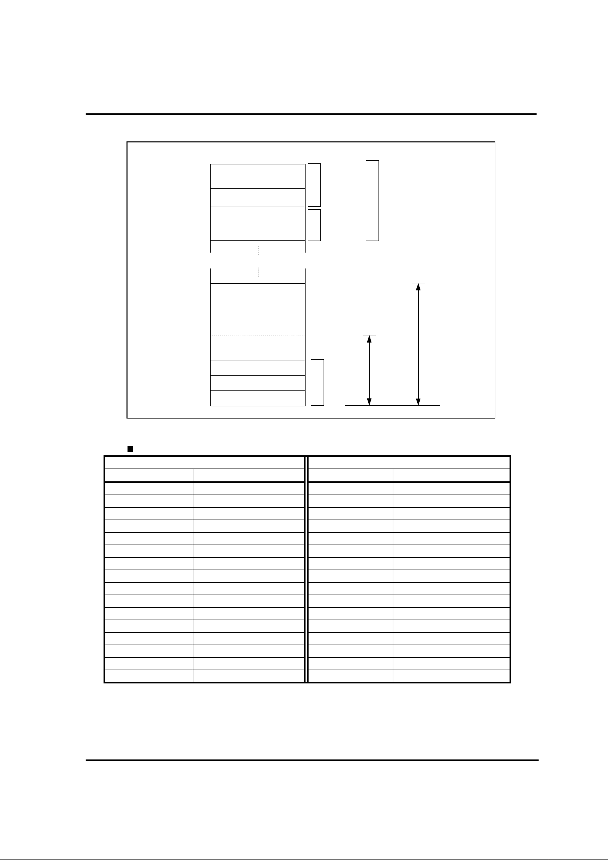
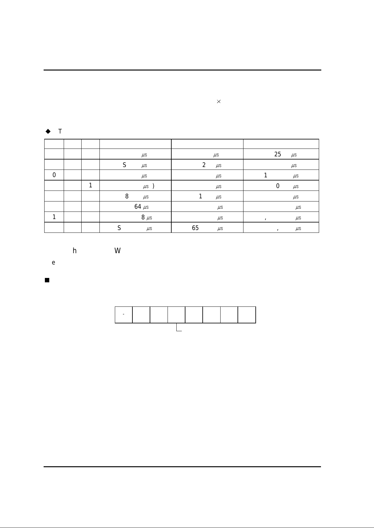
2.2.4. Peripheral Register List
Address Register Name
SYMBOL R/W
RESET VALUE
76543210
00C0
H
R0 PORT DATA REGISTER
R0
R/W Undefined
00C1
H
R0 PORT I/O DIRECTION REGISTER
R0DD
W 00000000
00C2
H
R1 PORT DATA REGISTER
R0
R/W Undefined
00C3
H
R1 PORT I/O DIRECTION REGISTER
R0DD
W 00000000
00C4
H
R2 PORT DATA REGISTER
R0
R/W Undefined
00C5
H
R2 PORT I/O DIRECTION REGISTER
R0DD
W 00000000
00C6
H
R3 PORT DATA REGISTER
R0
R/W Undefined
00C7
H
R3 PORT I/O DIRECTION REGISTER
R0DD
W 00000000
00C8
H
R4 PORT DATA REGISTER
R4
R/W Undefined
00C9
H
R4 PORT I/O DIRECTION REGISTER
R4DD
W 00000000
00CA
H
R5 PORT DATA REGISTER
R5
R/W Undefined
00CB
H
R5 PORT I/O DIRECTION REGISTER
R5DD
W 00000000
00CC
H
R6 PORT DATA REGISTER
R6
R/W Undefined
00CD
H
R6 PORT I/O DIRECTION REGISTER
R6DD
W0000----
00D0
H
PORT R4 MODE REGISTER
PMR4
W 00000000
00D1
H
PORT R5 MODE REGISTER
PMR5
W--00----
00D2
H
TEST MODE REGISTER
TMR
W -----000
00D3
H
BASIC INTERVAL REGISTER
BITR
R Undefined
CLOCK CONTROL REGISTER
CKCTLR
W --010111
00E0
H
WATCH DOG TIMER
WDTR
W -0111111
00E2
H
TIMER MODE REGISTER 0
TM0
R/W00000000
00E3
H
TIMER MODE REGISTER 2
TM2
R/W00000000
00E4
H
TIMER0 DATA REGISTER
TDR0
R/W Undefined
00E5
H
TIMER1 DATA REGISTER
TDR1
R/W Undefined
00E6
H
TIMER2 DATA REGISTER
TDR2
R/W Undefined
00E7
H
TIMER3 DATA REGISTER
TDR3
R/W Undefined
00E8
H
A/D CONVERTER MODE REGISTER
ADCM
R/W --000001
00E9
H
A/D CONVERTER DATA REGISTER
ADR
R Undefined
00EA
H
SERIAL I/O MODE REGISTER
SIOM
R/W -0000001
GMS81508/16
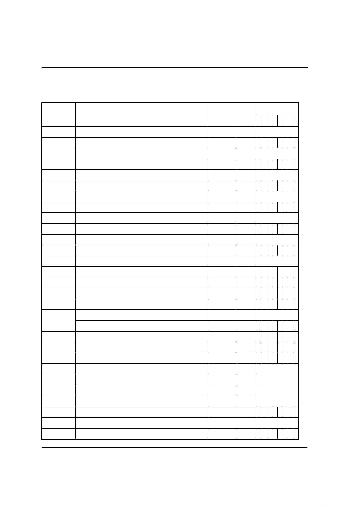
15
Address Register Name
SYMBOL R/W
RESET VALUE
76543210
00EB
H
SERIAL I/O REGISTER
SIOR
R/W Undefined
00EC
H
BUZZER DRIVER REGISTER
BUR
W Undefined
00F0
H
PWM0 DATA REGISTER
PWMR0
W Undefined
00F1
H
PWM1 DATA REGISTER
PWMR1
W Undefined
00F2
H
PWM CONTROL REGISTER
PWMCR
W00
00F3
H
INTERRUPT MODE REGISTER
IMOD
R/W --000000
00F4
H
INTERRUPT ENABLE REGISTER LOW
IENL
R/W 0000----
00F5
H
INTERRUPT REQUEST FLAG REGISTER LOW
IRQL
R/W 0000----
00F6
H
INTERRUPT ENABLE REGISTER HIGH
IENH
R/W00000000
00F7
H
INTERRUPT REQUEST FLAG REGISTER HIGH
IRQH
R/W00000000
00F8
H
EXT. INTERRUPT EDGE SELECTION REGISTER
IEDS
W 00000000
-: Not Used
Write Only Register can not be accessed by bit manipulation instruction.
HYUNDAI MicroElectronics
16
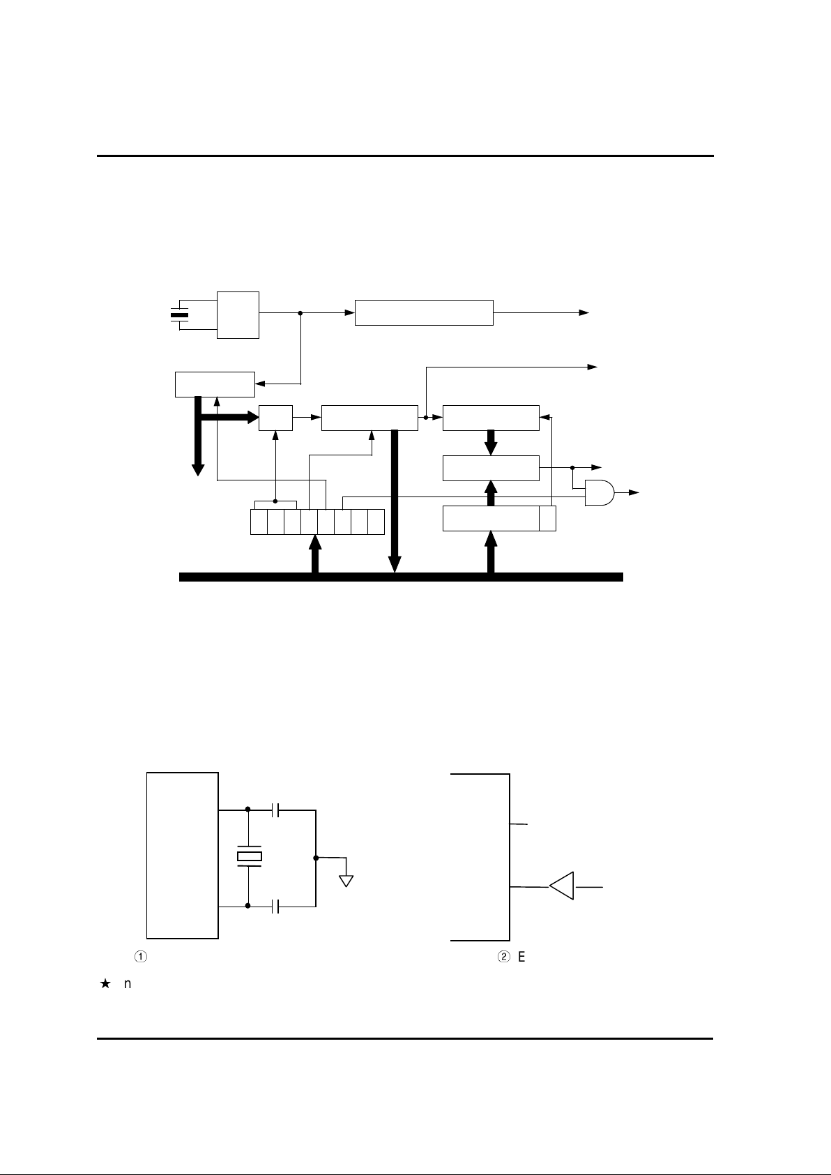
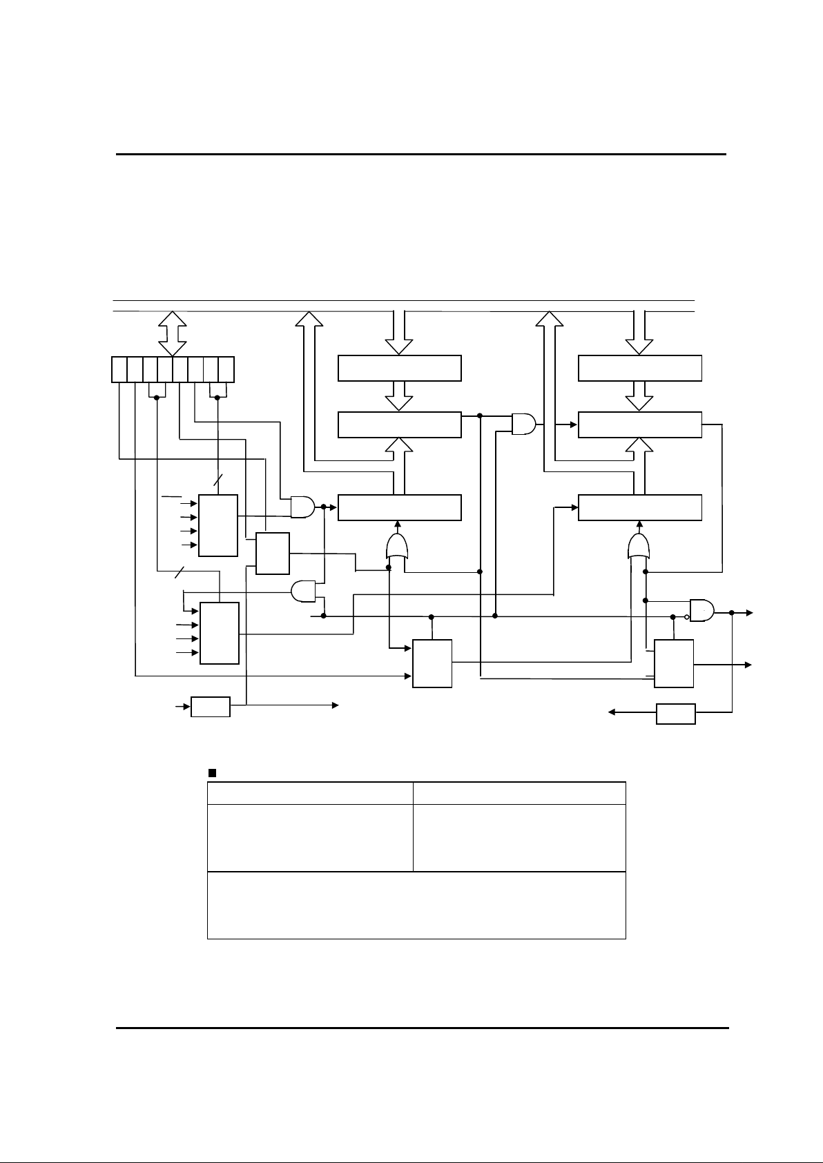
2.3. CLOCK GENERATION CIRCUIT
The clock generation circuit of GM S 81508/16 c onsists of oscillation circuit, prescaler , Basic Interval
Timer.
The source clock of peripherals is provided by 11-bit prescaler.
OSC
Circuit
Clock Pulse Generator
Prescaler
MUX B.I.T.(8) W.D.T.(6)
Comparator
WDTR
0 1 2 3 4 5 6 7
Internal System Clock
IFBIT
IFWDT
BTCL
ENPCK
WDTCL
To RESET
Circuit
Internal Data Bus
8
6
6
CKCTLR
6
2.3.1. Oscillation Circuit
The clock signal incoming from crystal osc illator or c er am ic r esonator via Xin and Xout or from
external clock via Xin is supplied to Clock Pulse Generator and P r escaler.
The internal system clock for CPU is made by Clock Pulse Generator, and several peripheral clock
is divided by prescaler.
The clock generation circuit of c ry stal oscillator or ceramic resonator is shown in below.
Crystal Oscillator or Ceramic Resonator External clock
In STOP Mode, The oscillation is stopped,
Xin pin goes to "L" level status, and Xout pin goes to "H" level state.
Xin
Cin
GND
Cout
Xout
Xin
External
Clock
Open
Xout
GMS81508/16
17
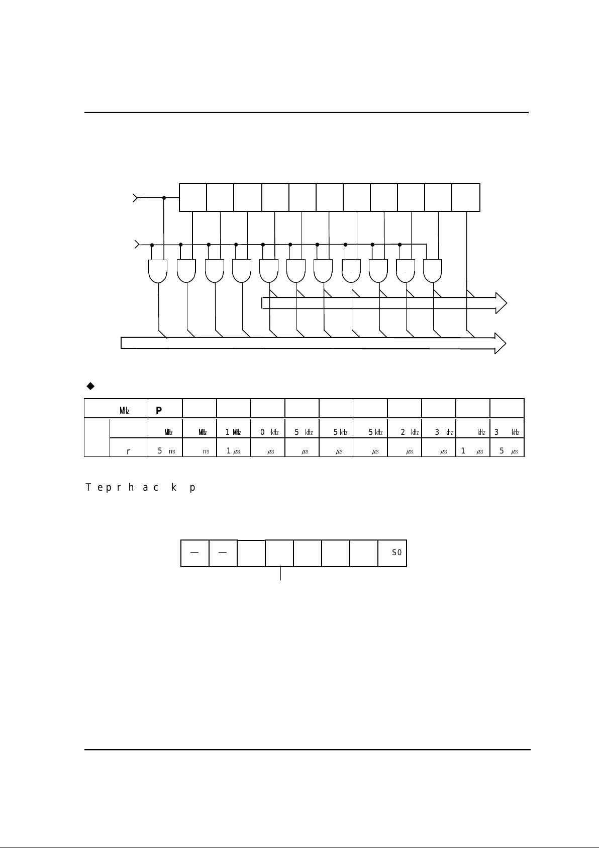
2.3.2. Prescaler
The prescaler consists of 11-bit bi nar y count er , and input clock is supplied by oscillation circuit. The
frequency div i ded by pr escaler is used as a source clock for peripherals.
Frequency- Divided Outputs of Prescal er
f
ex
()
PS1 PS2 PS3 PS4 PS5 PS6 PS7 PS8 PS9 PS10 PS11
Interval
4
2
1
500
250
12562.531.2515.367.183.59
Period
250
500
1
2
4
8
16
32
64
128
256
The peripheral cl oc k suppli ed from prescaler can be stopped by ENPCK. ( Howev er , PS 11 c annot
be stopped by ENPCK)
WWWWWW
76543210
8
Internal Data Bus
Peripherals
ENPCK
f
ex
B.I.T.
PS1 PS2 PS3 PS4 PS5 PS6 PS7 PS8 PS9 PS10 PS11
PS1 PS2 PS3 PS4 PS5 PS6 PS7 PS8 PS9 PS10
PS11
8
PS0
Enable Peripheral Clock
0 : stop
1 : supply
ENPCK
WDTON
BTCL BTS2 BTS1 BTS0
CKCTLR
<00D3H>
HYUNDAI MicroElectronics
18
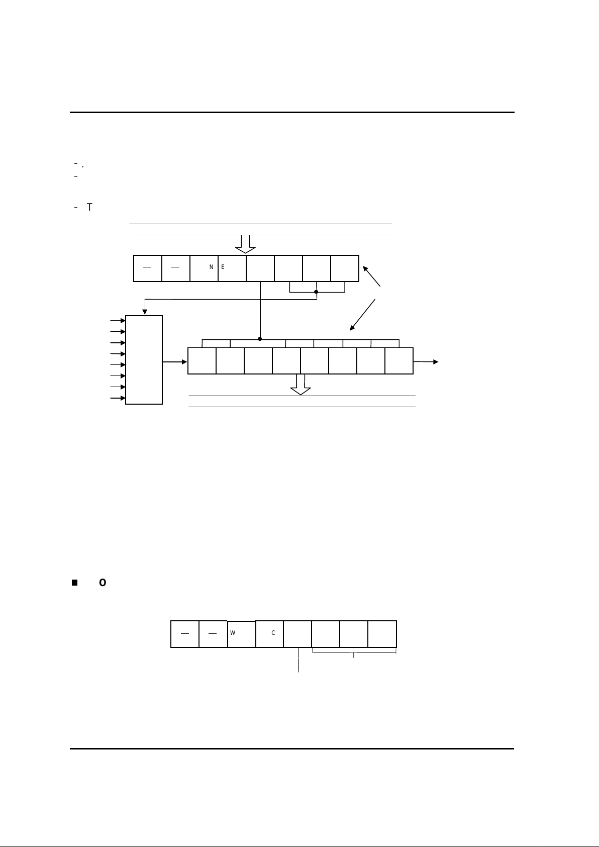
2.4. BASIC INTERVAL TIMER
The Basic Interval Timer(B .I.T.) has 8-bit binar y c ounter . The operations is shown below.
. Generates reference time interval interr upt request as a timer.
. The counting value of B.I.T. c an be r ead.
( Note; The writing at same address overwrites the CKCTLR.)
. The overflow of B.I.T be used the source c loc k of Watch Dog Timer.
2.4.1. Control of Basic Interval Timer
The Basic Interval Timer is free running timer. When the counting value is changed "0FFH" to
"00H" , The interrupt request flag is generated. The counter can be cleared by setting
BTCL
(Bit 3
of CKCTLR) and the BTCL is auto-cleared after 1 machine cy cle. The initial state (after Reset) of
BTCL is “0”.
The input clock of Basic Interval Timer is selec ted by B TS 2~BTS 0 ( Bit2~0 of CKCTLR) among the
prescaler outputs (PS4~PS 11).
The Basic Interval Timer Register (B ITR) c an be read.
The CKCTLR and the BITR have a same address (00D3H). So, If y ou wr ite to this addr es s, the
CKCTLR would be controlled. If you read this address, the c ounting value of B ITR would be read.
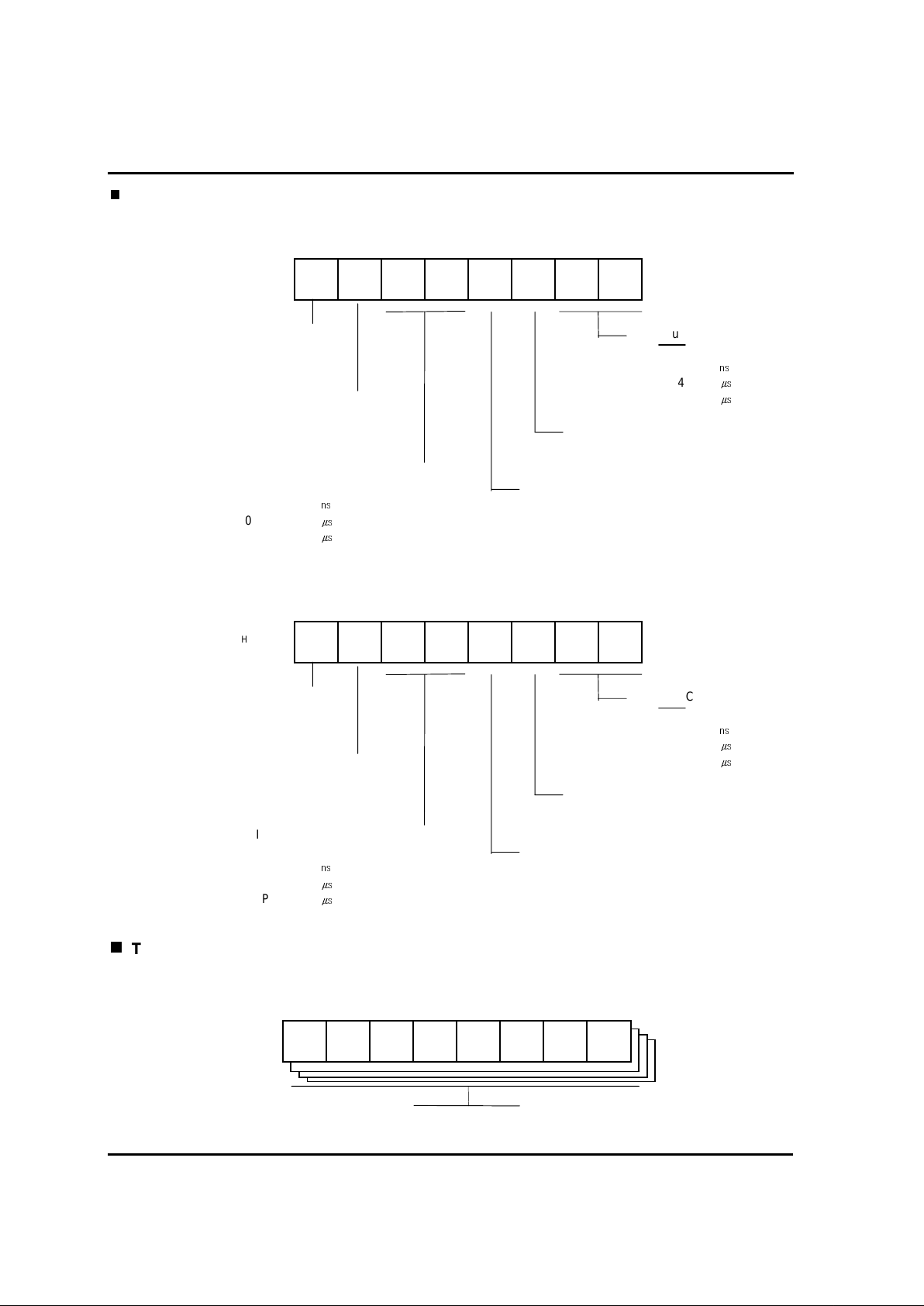
CLOCK CONTROL REGISTER
PS4
WDTON ENPCK
BTCL BTS2 BTS1 BTS0
CKCTLR
bit7 bit6
bit5 bit4
bit3 bit2 bit1 bit0
BITR
PS5
PS6
PS7
PS8
PS9
PS10
PS11
MUX
IFBIT
Internal Data Bus
Internal Data Bus
Same address
when read, it can be read as
counter value. When write, it can
be write as control register.
B.I.T. input clock selection
B.I.T. CLEAR ( When writing )
0 : B.I.T. Free-run
1 : B.I.T. Clear ( auto cleared after 1 machine cycle )
7
6
5 4
ENPCKWDTON
3
BTCL
2
BTS21BTS10BTS0
W W W W W W
<00D3H>
CKCTLR
GMS81508/16
19
BASIC INTERVAL TIM E R DATA REGISTER
2.5. WATCH DOG TIMER
The Watch Dog Timer is a means of recover y from a system problem.
In this Device, the Watch Dog Timer consists of 6-bit binary count er , 6-bit comparator and watch
dog timer regi ster (WDTR). The source clock of WDT is overflow of Basi c Interval Timer. The
interrupt request of WDT is generated when the counting value of WDT equal to the contents of
WDTR( bit0~5). T his can be used as s/w int er r upt or MICOM RESET signal(Watch Dog Function).
2.5.1. Control of Watch Dog Timer
It can be used as 6-bit timer or WDT according to bit5(WDTON) of Clock Control Register
(CKCTLR). The counter can be cleared by setting WDTC L ( Bit 6 of WDTR) and the WDTCL is
auto-cleared after 1 machine cycle. The initi al state (after Reset) of WDTCL is “0”.
CLOCK CONTROL REGISTER
WATCH DOG TIMER REGISTER
WDT ON
0 : 6-bit Timer
1 : Watch Dog Timer
7
6
5 4
ENPCK
WDTON
3
BTCL2BTS21BTS10BTS0
W W W W W W
<00D3H>
CKCTLR
Watch Dog Timer Clear
0 : free run
1 : W.D.T counter clear
7
6
WDTCL
5
WDTR5
4 3 2 1 0
W W W
W W W W W
<00E0H>
WDTR
Determines the interval of W.D.T Interrupt
WDTR3WDTR4 WDTR0WDTR1WDTR2
B.I.T data
7
6
5 4
3
2
1
0
R
R
R R R R R R
<00D3H>
BITR
HYUNDAI MicroElectronics
20
The interval of WDT interr upt is decided by the interrupt interval of Basic Interval Timer and the
contents of WDTR.
The interval of WDT = The contents of WDTR The interval of B.I.T.
Caution) Do not use the contents of WDTR = "0"
The relationship between the input clock of B.I.T and the output of W.D.T. (@8MHz)
BTS2BTS1BTS0 B.I.T. Input Clock The cycle of B .I.T. The cycle of W.D.T.(max)
000
PS4 ( 2 ) 512
32,256
001
PS5 ( 4 ) 1,024
64,512
010
PS6 ( 8 ) 2,048
129,024
011
PS7 ( 16 ) 4,096
258,048
100
PS8 ( 32 ) 8,192
516,096
101
PS9 ( 64 ) 16,384
1,032,192
110
PS10 ( 128 ) 32,768
2,064,384
111
PS11 ( 256 ) 65,536
4,128,768
2.5.2. The output of WDT signal
The overflow of WDT can be output through R54/WDT O port by setting bit4 of P M R5( WDTS ) to
"1".
PORT R5 MODE REGISTER
<00D1H>
PMR5
7
-
6
-5BUZS
4
WDTS
3
-
2
-
1
-
0
-
WW
R54/WDT O Selection
0 : R54 ( Input / Output )
1 : WDTO ( Output )
GMS81508/16
21
2.6. TIMER
The GMS81508/16 has four multi-functional 8-bit bi nar y timers(Timer0~Timer 3).
Timer0 (or Timer2) is can be used as a 16-bit timer/event counter wit h Timer 1(or Timer3). The
Timer0-1 and Tim er 2- 3 hav e same f uncti ons and structures. So, We will explains about Timer0 and
Timer1 only.
Operation Mode of Timer
Timer0,Timer2 Timer1,Timer3
-. 8-bit Interval Timer
-. 8-bit Event Counter
-. 8-bit input capture
-. 8-bit Interval Timer
-. 8-bit rectangular pulse
output
-. 16-bit Interval Timer
-. 16-bit Event Counter
-. 8-bit r ectangular pulse output
ck
PS6
T0CN
T1ST
INT0
CAP0
T0ST
PS6
2
TDR0
16bit Mode
16bit Mode
MUX
8
TM0
7
1 03 25 47 6
TDR1
IFT0
INTR0
T1O
IFT1
8
8
Comparator 0
8
Comparator 1
Data Reg. 1Data Reg. 0
8
T 0
8
T 1
8 8
Clea
ck
Clea
1
MUX
0
0
MUX
1
F / F
EDGE
1
MUX
0
MUX
2
HYUNDAI MicroElectronics
22
TIMER MODE REGISTER 0,2(TM0,TM2)
TIMER DATA REGISTER(TDR0 ~ TDR3)
T1 Input Clock Selection
00 : Connection to T0 (16bit Mode )
01 : PS2 ( 500)
10 : PS4 ( 2)
11 : PS6 ( 8)
T3 Input Clock Selection
00 : Connection to T2 (16bit Mode )
01 : PS2 ( 500)
10 : PS4 ( 2)
11 : PS6 ( 8)
T0 Input Clock Selection
00 : EC0
01 : PS2 ( 500)
10 : PS4 ( 2)
11 : PS6 ( 8)
T2 Input Clock Selection
00 : EC2
01 : PS2 ( 500)
10 : PS4 ( 2)
11 : PS6 ( 8)
<00E2H>
<00E3H>
TM0
TM2
7
7
CAP0
CAP2
6
6
T1ST
T3ST
5
5
T1SL1
T3SL1
4
4
T1SL0
T3SL0
3
3
T0ST
T2ST
2
2
T0CN
T2CN
1
1
T0SL1
T2SL1
0
0
T0SL0
T2SL0
R/W
R/W
R/W
R/W
R/W
R/W
R/W
R/W
R/W
R/W
R/W
R/W
R/W
R/W
R/W
R/W
T0 Start/Stop control
0 : Count Stop
1 : Counting start after clearing T0
T2 Start/Stop control
0 : Count Stop
1 : Counting start after clearing T2
T0 Start/Stop control
0 : COUNT Stop
1 : COUNT Start
T2 Start/Stop control
0 : COUNT Stop
1 : COUNT Start
Input Capture Selection
0 : Timer/Counter
1 : Input Capture
Input Capture Selection
0 : Timer/Counter
1 : Input Capture
T1 Start/Stop control
0 : Cout Stop
1 : Counting start after clearing T1
T3 Start/Stop control
0 : Cout Stop
1 : Counting start after clearing T3
TDR0~3
7 6 5 4 3 2 1 0
R/W R/W R/W R/W R/W R/W R/W R/W
( WRITE)
Modulo Data Write
( READ )
Count Value Read
<00E4H~00E7H >
GMS81508/16
23
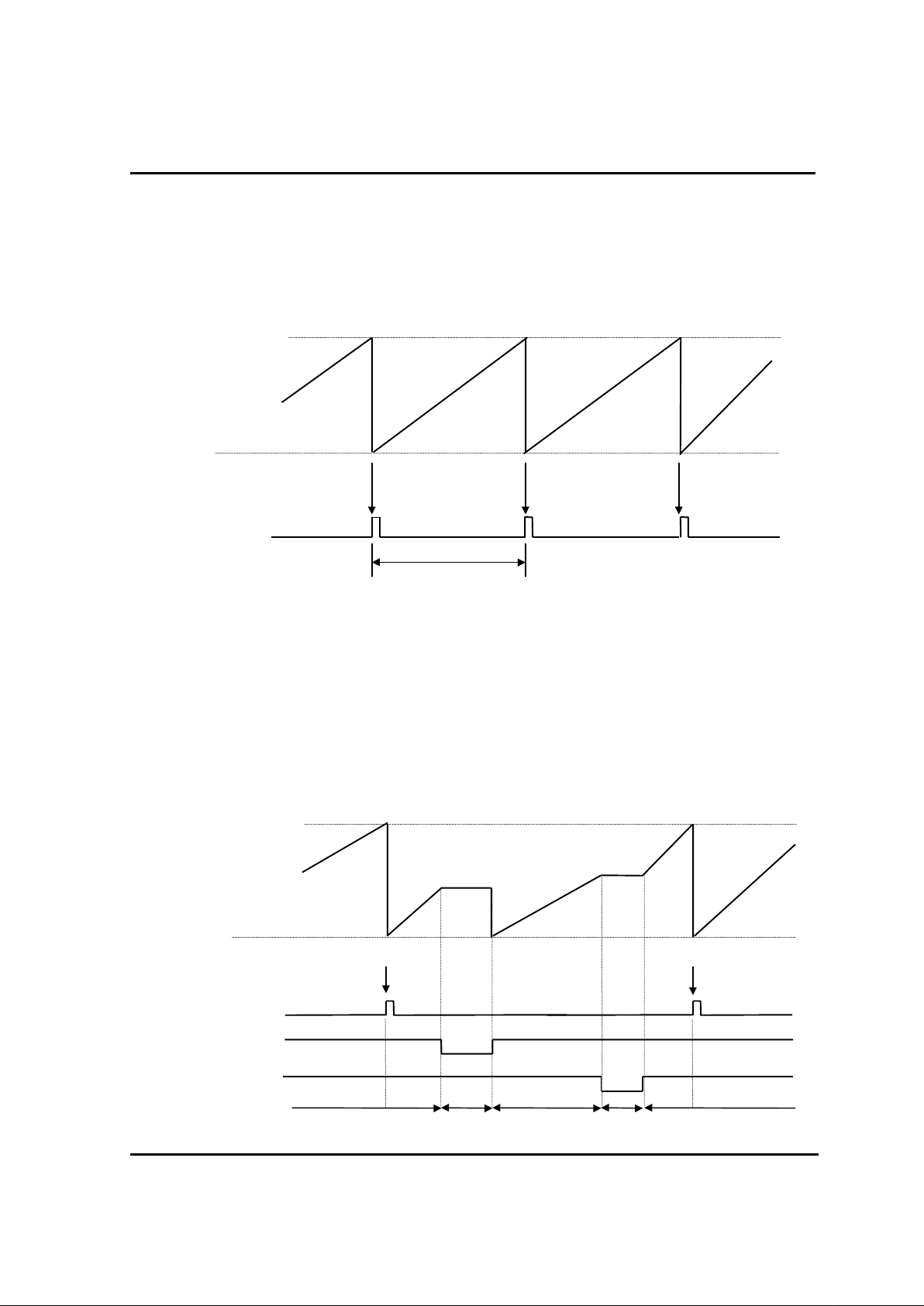
2.6.1. Control of Timer
T0 ( T1 ) consists of 8-bit Binary Up-Counter. When the counting value of Timer0 , Timer1 and
Timer0-1(16bit) become equal to the contents of Timer Data Register(TDR0,TDR1,TDR0-1) v alue,
the counter is cl ear ed to "00H" and restarts count-up operati on. At this time, Interrupt request ( IFT0
or IFT1) is generated.
Any of the PS2, PS4, PS6 or external clock can be selected as the clock source of T0 by
bit1(T0SLI) and bit0(T0SL0) of TM0. Any of the PS 2, PS4, PS6 or ov erflow of T0 can be selected
as the clock source of T1 by bit5( T1SL1) and bit4(T1SL0) of TM0. When the overflow of T0 is
selected as input cl oc k of T1, Timer 0-1 operates as 16 -bit timer. In thi s case, Timer0-1 only is
controlled by T0ST,T0CN and the interrupt vector is Timer0 vector.
The operation of T0, T1 is cont r olled by bit3(T0ST), bit2(T 0CN) and bi t6(T1ST) of TM0. T0CN
controls count stop/start without cleari ng c ounter. T0ST and T1ST control count stop/star t after
timer clear. In order to enable count-up of timer , T0CN, T0ST and T1ST should become “1”. In
order to start c ount-up after clearing of counter, T 0ST or T1ST shoul d be set to "1" after set to "0"
temporarily .
Interval Period
InterruptInterruptInterrupt
MATCHMATCHMATCH
ClearClearClear
00
H
IFT0
T0 VALUE
TDR0 VALUE
Count
Count
StopCountStop
“0” “1” Start
“0” “1” Clear & Start
InterruptInterrupt
MATCHMATCH
ClearClearClear
00
H
IFT0
T0 VALUE
TDR0 VALUE
T0ST
COUNTER
T0CN
 Loading...