

HEI GMS81024, GMS81008, GMS81016, GMS81032, GMS81004 Datasheet

8-BIT SINGLE CHIP MICROCOMPUTERS
GMS810 SERIES
USER`S MANUAL
• GMS81004
• GMS81008
• GMS81016
• GMS81024
• GMS81032

Revision 3.0
Published by
MCU Application Team in HYUNDAI ELCETRONICS Co., Ltd.
¨Ï
HYUNDAI ELECTRONICS Co., Ltd. 1998 All Right Reserved.
Additional information of this manual may be served by HYUNDAI ELECTIONICS Offices in Korea or
Distributors and Representative listed at address directory.
HYUNDAI ELECTIONICS reserves the right to make changes to any Information here in at any time
without notice.
The information, diagrams, and other data in this manual are correct and reliable; however, HYUNDAI
ELECTIONICS Co., Ltd. is in no way responsible for any violations of patents or other rights of the
third party generated by the use of this manual.

Table of Contents
Chapter 1
Overview
1.1 Features & Pin Assignments . . . . . . . . . . . . . . . . . . . . . 1-1
1.2 Block Diagram . . . . . . . . . . . . . . . . . . . . . . . . . . . . . . . 1-2
1.3 Package Dimension . . . . . . . . . . . . . . . . . . . . . . . . . . . 1-3
1.4 Pin Function . . . . . . . . . . . . . . . . . . . . . . . . . . . . . . . . . 1-5
1.5 Port Structure . . . . . . . . . . . . . . . . . . . . . . . . . . . . . . . . 1-6
1.6 Electrical Characteristics . . . . . . . . . . . . . . . . . . . . . . . . 1-10
Chapter 2
Function Description
Table of Contents
2.1 Register . . . . . . . . . . . . . . . . . . . . . . . . . . . . . . . . . . . . 2-1
2.2 Memory Map . . . . . . . . . . . . . . . . . . . . . . . . . . . . . . . . . 2-6
2.3 TCALL Vector Area . . . . . . . . . . . . . . . . . . . . . . . . . . . 2-7
2.4 Zero-Page Peripheral Registers . . . . . . . . . . . . . . . . . . . 2-8
Chapter 3
I/O PORT
3.1 Port R0 . . . . . . . . . . . . . . . . . . . . . . . . . . . . . . . . . . . . . . 3-1
3.2 Port R1 . . . . . . . . . . . . . . . . . . . . . . . . . . . . . . . . . . . . . . 3-2
3.3 Port R2 . . . . . . . . . . . . . . . . . . . . . . . . . . . . . . . . . . . . . . 3-2
Chapter 4
Peripheral Hardware
4.1 Clock Generating Circuit . . . . . . . . . . . . . . . . . . . . . . . . . 4-1
4.2 Timer . . . . . . . . . . . . . . . . . . . . . . . . . . . . . . . . . . . . . . 4-10

Table of Contents
Chapter 5
Interrupt
5.1 Interrupt Source . . . . . . . . . . . . . . . . . . . . . . . . . . . . . . . 5-1
5.2 Interrupt Control Register . . . . . . . . . . . . . . . . . . . . . . . . 5-3
5.3 Interrupt Accept Mode . . . . . . . . . . . . . . . . . . . . . . . . . . . 5-4
5.4 Interrupt Processing Sequence . . . . . . . . . . . . . . . . . . . . 5-7
5.5 Software Interrupt . . .. . . . . . . . . . . . . . . . . . . . . . . . . . . 5-8
5.6 Multiple Interrupt . . . . . . . . . . . . . . . . . . . . . . . . . . . . . . 5-9
5.7 Key Scan Input Processing . . . . . . . . . . . . . . . . . . . . . . . 5-11
Chapter 6
Standby Function
6.1 Stop Mode . . . . . . . . . . . . . . . . . . . . . . . . . . . . . . . . . 6-1
6.2 Standby Mode Release . . . . . . . . . . . . . . . . . . . . . . . . . 6-3
6.3 Release Operation of Standby Mode . . . . . . . . . . . . . . . 6-5
Chapter 7
Reset Function
7.1 External RESET . . . . . . . . . . . . . . . . . . . . . . . . . . . . . . . 7-1
7.2 Power On Reset . . . . . . . . . . . . . . . . . . . . . . . . . . . . . . . 7-1
7.3 Low Voltage Detection Mode . . . . . . . . . . . . . . . . . . . . . 7-4
Appendix
Instruction Set Table
Programmer`s guide
Mask option list
OVERVIEW 1
FUNCTION DESCRIPTION 2
I/O PORT 3
PERIPHERAL HARDWARE 4
INTERRUPT 5
STANDBY FUNCTION 6
RESET FUNCTION 7
APPENDIX A. 8
APPENDIX B. 9

Chapter 1. Overview
CHAPTER 1. OVERVIEW
The GMS810 Series is the high speed and Low voltage operating 8-bit single chip
microcomputers. This MCU contains G8MC core, ROM, RAM, input/output ports and five
multi-function timer/counters.
1.1 FEATURES & PIN ASSIGNMENTS (TOP VIEW)
¡á
ROM size . . . . . . . . . . . . . 4,096 Bytes ( GMS81004 ) , 8,192 Bytes (GMS81008 )
. . . . . . . . . . . . . 16,384 Bytes ( GMS81016 ) ,24,576 Bytes(GMS81024 )
. . . . . . . . . . . . . 32,768 Bytes ( GMS81032 )
¡á
RAM size . . . . . . . . . . . . . 448 Bytes
¡á
Instruction Execution Time . . 1us @Xin=4MHz
¡á
Timer
¡Ü Timer/Counter . . . . . . 8Bit * 2ch , 16Bit * 1ch
¡Ü Basic Interval Time . . . 8Bit * 1ch
¡Ü Watch Dog Timer . . . . 6Bit * 1ch
¡á
Power On Reset
¡á
Power Saving Operation Modes
¡Ü STOP
¡á
8 Interrupt Sources
¡Ü Nested Interrupt Control is Available
¡á
Operating Voltage
¡Ü 2.0~4.0V @2MHz
¡Ü 2.2~4.0V @4MHz
¡á
Low Voltage Detection Circuit
¡á
Watch dog Timer Auto Start ( During 1Second after Power on Reset )
¡á
Package
¡Ü 20SOP/20PDIP/24SOP/24Skinny DIP/28SOP/28Skinny DIP
¡Ü 44PLCC
¡á
I/O Port
20pin 24pin 28pin 44pin
input 3 3 3 3
output 2 2 2 2
I/O 13 17 21 24
1 - 1
Chapter 1. Overview
PIN ASSIGNMENT
R13
R12
R11
R10
VDD
XOUT
XIN
R00
R01
R02
R03
R20
R21
R22
1
2
3
4
5
6
7
28PIN
8
9
10
11
12
13
14
28
R14
27
R15
26
R16
25
R17
24
REMOUT
23
RESET
22
TEST
21
R07
20
R06
19
R05
18
R04
17
VSS
16
R24
15
R23
NC
R17
R16
R15
R14
NC
R13
R12
R11
R10
NC
40
41
42
43
44
1
2
3
4
5
6
1
R13
2
R12
3
R11
4
R10
5
VDD
6
XOUT
XIN
R00
R01
R02
R03
R20
NC
3938373635343332313029
24PIN
7
24PIN 20PIN
8
9
10
11
12
REMOUT
RESET
R27
VSS
24
23
22
21
20
19
18
17
16
15
14
13
NC
TEST
R14
R15
R16
R17
REMOUT
RESET
TEST
R07
R06
R05
R04
VSS
44PLCC
R07
R06
R05
R11
R10
VDD
XOUT
XIN
R00
R01
R02
R03
R20
NC
1
2
3
4
5
6
7
8
9
10
28
NC
27
R04
26
VSS
25
R24
24
R23
23
NC
22
R22
21
R21
20
R20
19
R03
18
NC
20
R16
19
R17
18
REMOUT
17
RESET
16
TEST
15
R07
14
R06
13
R05
12
R04
11
VSS
7
NC
8
VDD
9
XOUT
1011121314
NC
R00
R25
XIN
1 - 2
151617
R26
R01
R02
NC
1.2 Block Diagram
Chapter 1. Overview
REMOUT
R17/T0
R16/T1
R15/T2
R14/EC
R12/INT2
R11/INT1
R00~R07
R10~R17
TEST
RESET
Xin
Xout
WATCHDOG
TIMER
TIMER
INTERRUPT
Key scan
INT.
generation
Block
CLOCK
GEN. /
SYSTEM
CONTROL
G8MC
CORE
RAM
(448byte)
`
ROM
(16K byte)
PRESCALER
/
B.I.T
R0
R00~R07
PORT
R1
R10~R17
PORT
R2
R20~R27
PORT
Vdd Vss
1 - 3
Chapter 1. Overview
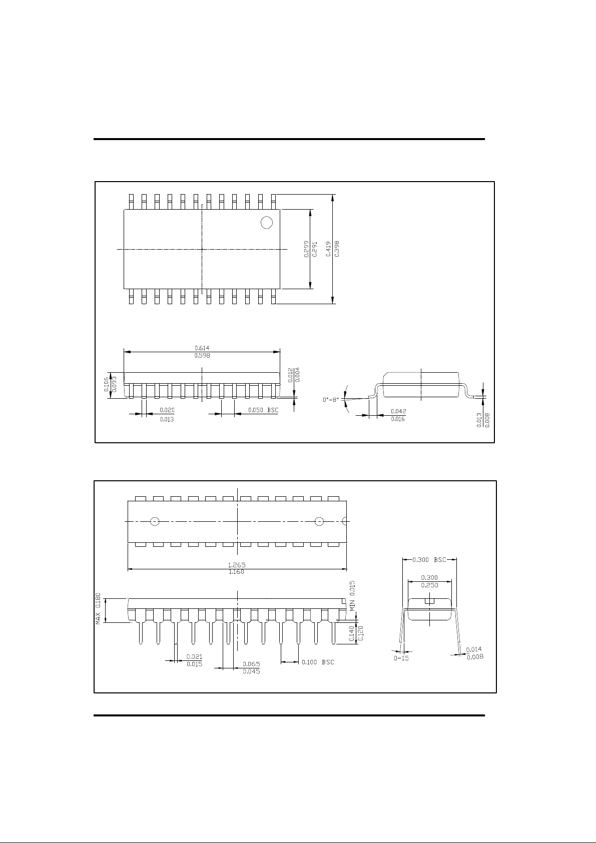
1.3 Package Dimension
1.3.1 20SOP Pin Dimension(dimensions in inch)
1.3.2 20PDIP Pin Dimension (dimensions in inch)
1 - 4
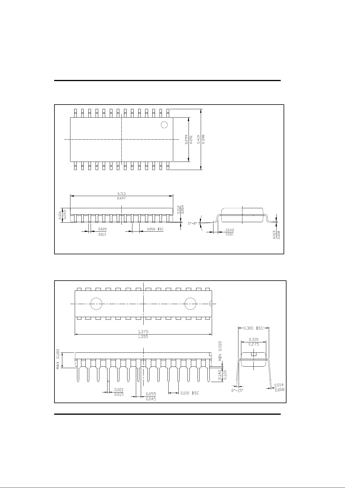
1.3.3 24SOP Pin Dimension (dimensions in inch)
Chapter 1. Overview
1.3.4 24skinnyDIP Pin Dimension (dimensions in inch)
1 - 5
Chapter 1. Overview
1.3.5 28SOP Pin Dimension (dimensions in inch)
1.3.6 28skinnyDIP Pin Dimension (dimensions in inch)
1 - 6
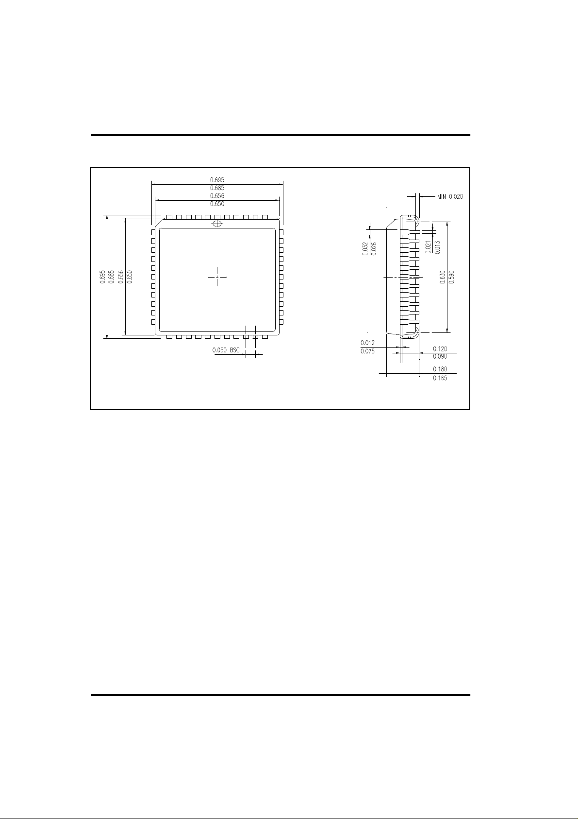
1.3.7 44PLCC Pin Dimension (dimensions in mm)
Chapter 1. Overview
1 - 7
Chapter 1. Overview
1.4 Pin Function
PIN NAME
R00 I/O
R01
R02
R03
R04
R05
R06
R07
R10
R11/INT1
R12/INT2
R13
R14/EC
R15/T2
R16/T1
R17/T0
R20
R21
R22
R23
R24
R25 I/O
R26 I/O
R27 I/O
XIN
XOUT
REMOUT
RESET
TEST
VDD
VSS
VSS P
INPUT/
OUTPUT
I/O
I/O
I/O
I/O
I/O
I/O
I/O
I/O
I/O
I/O
I/O
I/O
I/O
I/O
I/O
I/O
I/O
I/O
I/O
I/O
I
O
O
I
I
P
P
INPUT
20Pin 24Pin 28Pin 44Pin
6 8 8 11
7 9 9 15
8 10 10 16
9 11 11 19
12 14 18 27
13 15 19 30
14 16 20 31
15 17 21 32
2 4 4 5
1 3 3 4
- 2 2 3
- 1 1 2
- 24 28 44
- 23 27 43
20 22 26 42
19 21 25 41
10 12 12 20
- - 13 21
- - 14 22
- - 15 24
- - 16 25
- - - 13
- - - 14
- - - 36
5 7 7 10
4 6 6 9
18 20 24 38
17 19 23 37
16 18 22 33
3 5 5 8
11 13 17 26
- - - 35
Function @ RESET @ STOP
- Each bit of the port can be
individually configured as an
input or an output by user
software
- Push-pull output
- CMOS input with pull-up resistor
(option)
- Can be programmable as Key
Scan Input
- Pull-ups are automatically
disabled at output mode
- CMOS input with pull-up resistor
(option)
- Push-pull output
- Can be programmable as Key
Scan Input or Open drain output
- Direct Driving of LED(N-TR)
- Pull-ups are disabled at output
mode
- CMOS input with pull-up resistor
(option)
- Push-pull output
- Direct Driving of LED(N-TR)
- Pull-ups are disabled at output
mode
- Oscillator Input
- Oscillator Output
- High Current Output
- Includes pull-up resistor
- Includes pull-up resistor
- Positive power supply
- Ground
INPUT
INPUT
INPUT
`L` output
`L` level
State
of before
STOP
State
of before
STOP
State
of before
STOP
Low
High
`L` Output
state
of before
STOP
1 - 8
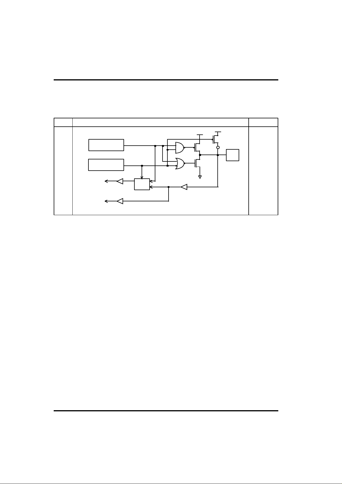
1.5 Port Structure
1.5.1 R0 PORT
Chapter 1. Overview
PIN @ RESET
Data Reg
R00
R01
R02
R03
R04
R05
R06
R07
Direction Reg
Data Bus
¡è
Rd
Data Bus
¡è
Rd
CIRCUIT TYPE
MUX
VDD
VSS
VDD
pull-up
option
PAD
Hi - Z
OR
High-Input
(with pullup)
1 - 9
Chapter 1. Overview
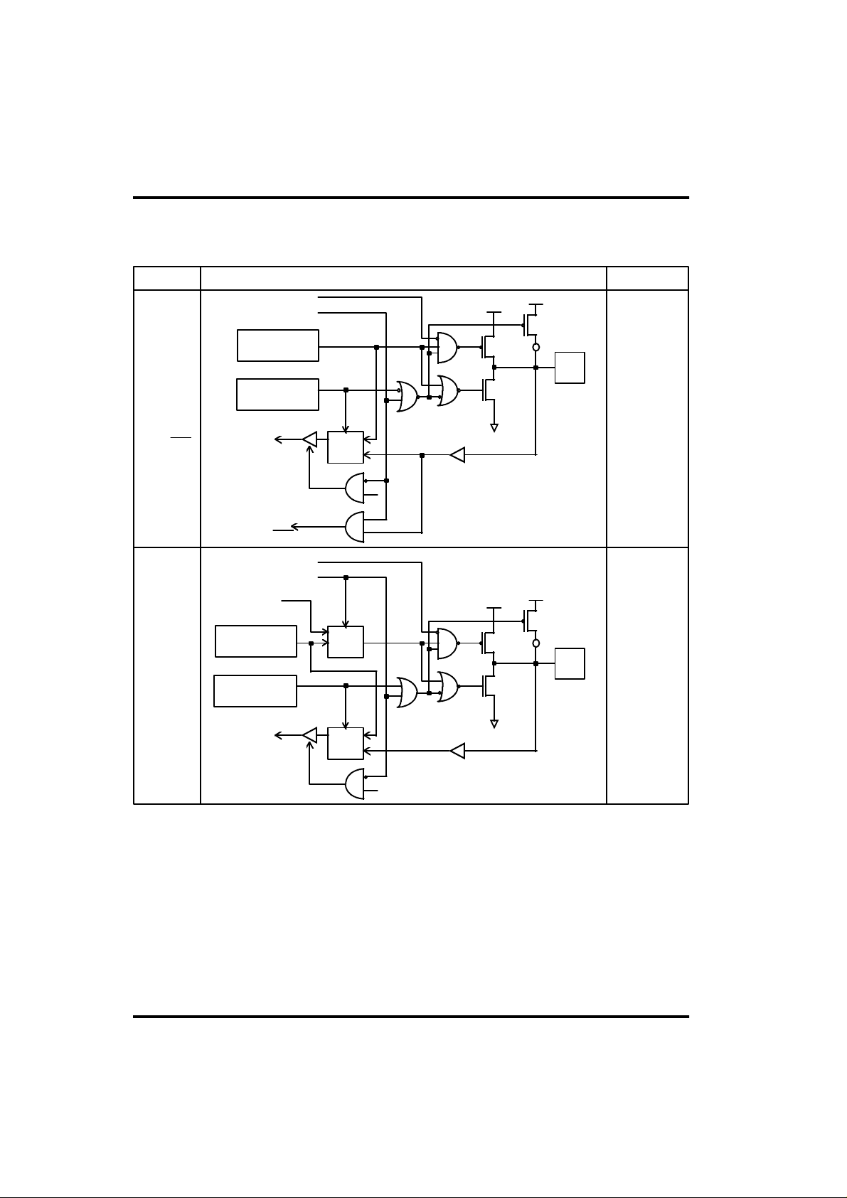
1.5.2 R1 PORT
PIN CIRCUIT TYPE @ RESET
VSS
VDD
pull-up
option
PAD
High-Input
(with pullup)
R10
R11/INT1
R12/INT2
R13
R14/EC
open drain
selection
Data Reg
Direction Reg
Data Bus
VDD
MUX
Hi - Z
OR
R15 / T2
R16 / T1
R17 / T0
T0 R11...INT1
T0 R12...INT2
T0 R14...EC
open drain
selection
from R15...T2
from R16...T1
from R17...T0
Data Reg
Direction Reg
Data Bus
MUX
MUX
Rd
Rd
VDD
VSS
VDD
pull-up
option
PAD
Hi - Z
OR
High-Input
(with pullup)
1 - 10
Chapter 1. Overview
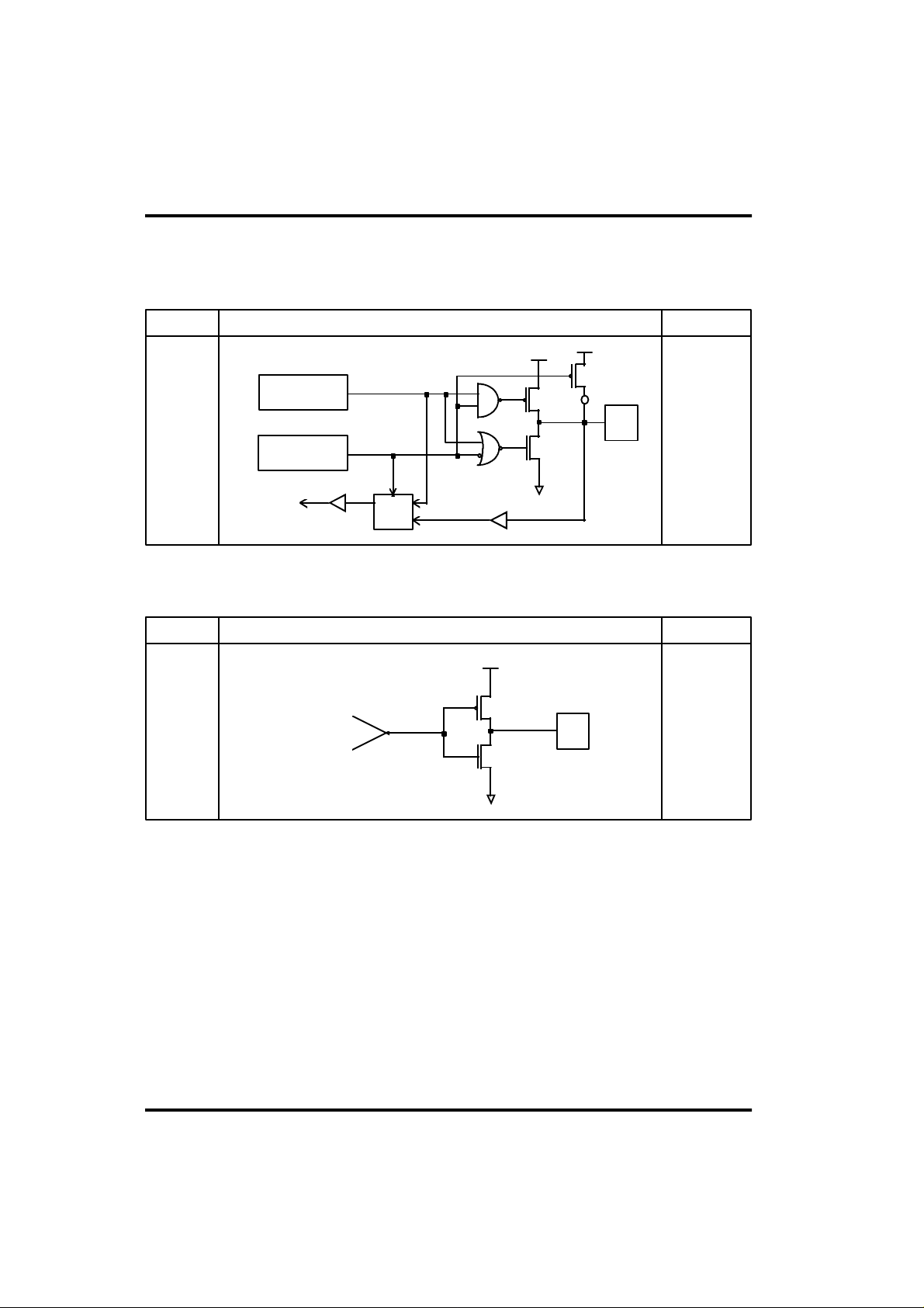
1.5.3 R2 PORT
PIN CIRCUIT TYPE @ RESET
VDD
pull-up
option
PAD
High-Input
(with pullup)
VSS
R20
R21
R22
R23
R24
R25
R26
R27
Data Reg
Direction Reg
Data Bus
¡è
Rd
VDD
MUX
REMOUT PORT
PIN CIRCUIT TYPE @ RESET
Hi - Z
OR
REMOUT
internal signal
VDD
VSS
PAD
Low level
1 - 11
Chapter 1. Overview
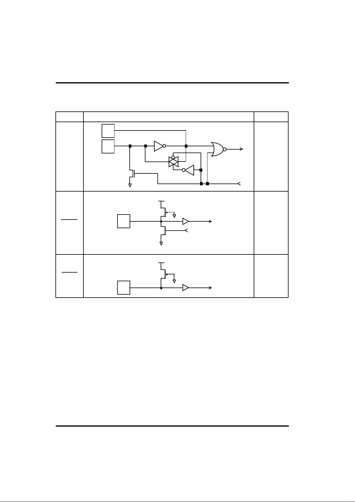
1.5.4 Miscellaneous Ports
PIN CIRCUIT TYPE @ RESET
Xout
Xin
Xin
Xout
RESET
from STOP circuit
VSS
VDD
pull-up resistor
VSS
PAD
from POWER on RESET circuit
VSS
oscillation
Low level
VDD
TEST High level
PAD
pull-up resistor
VSS
1 - 12
1.6 Electrical Characteristics
1.6.1 Absolute Maximum Ratings (Ta = 25¡É)
Chapter 1. Overview
PARAMETER
Supply Voltage
Input Voltage
Output Voltage
Operating Temperature
Storage Temperature
1.6.2 Recommended Operating Ranges
Power Dissipation
SYMBOL
VDD
VI
VO
Topr
Tstg
PD
RATINGS
-0.3 ~ +7.0
-0.3 ~ VDD + 0.3
-0.3 ~ VDD + 0.3
0 ~ 70
-65 ~ 150
700
1.6.2 Recommended Operating Ranges
PARAMETER SYMBOL CONDITION UNIT
VDD1
Supply Voltage
VDD2
Oscillation Frequency fXin
Operating Temperature Topr
fXin = 1MHz
fXin = 2MHz
fXin = 4MHz
MIN. TYP. MAX.
2.0
2.2 4.0
0 70
4.0
4.02.01.0
UNIT
V
V
V
¡É
¡É
mW
V
V
MHz
¡É
1 - 13
Chapter 1. Overview
1.6.3 DC Characteristics (VDD = 2.0~4.0, Vss = 0V, Ta = 0¡É ~ 70¡É)
Parameter Symbol Condition
high level
input voltage
low level
input voltage
high level input
leakage current
low level input
leakage current
high level
output voltage
low level
output voltage
high level output
leakage current
low level output
leakage current
high level output
current
low level output
current
input pull-up
current
POWER
SUPPLY
CURRENT
RAM retention
supply voltage
VIH1 R11, R12, R14, RESETB
VIH2
VIL1 R11, R12, R14, RESETB
VIL2 R0, R1(Except R11,R12,R14 ) , R2
IIH
R0,R1,R2,RESETB
R0,R1,R2,RESETB
IIL
(without pull-up)
VOH1
VOH2
VOH3
VOH5 OSC IOH=-200uA VDD-0.9 V
VOL1
VOL2
VOL5 OSC IOL=200uA 0.8 V
IOHL
IOLL
ISTOP
VRET 0.7 V
R0
R1(ExceptR17),R2
R17
R0
R1, R2
R0, R1, R2
R0, R1, R2
IOH REMOUT VOH=2V -30 -12 -5 mA
IOL REMOUT VOL=1V 0.5
IP1 RESETB
IP2 R0, R1, R2
fXIN=4MHz
operating
IDD
current
fXIN=2MHz
stop
mode
current
oscillator
stop
VIH=VDD
VIL=0V
IOH=-0.5mA
IOH=-1mA
IOH=-8mA
IOL=1mA
IOL=5mA
VOH=VDD
VOL=0V
VDD=3V
VDD=3V
VDD=4V
VDD=2.2V
VDD=4V
VDD=2V
VDD=4V
VDD=2V
Specification
VDD-0.4
VDD-0.4
VDD-0.9
---
---
-
maxtypmin
VDD0.8VDD
0.2VDD0
0.3VDD0
1
-1uAuA
0.4
0.8
1
-1uAuA
3 mA
603015
402010
104
62.4
62.4
31.2
103
82
Unit
V
VVDD0.7VDDR0, R1(Except R11,R12,R14 ) , R2
V
V
V
V
V
V
V
uA
uA
mA
mA
mA
mA
uA
uA
1 - 14
Chapter 1. Overview
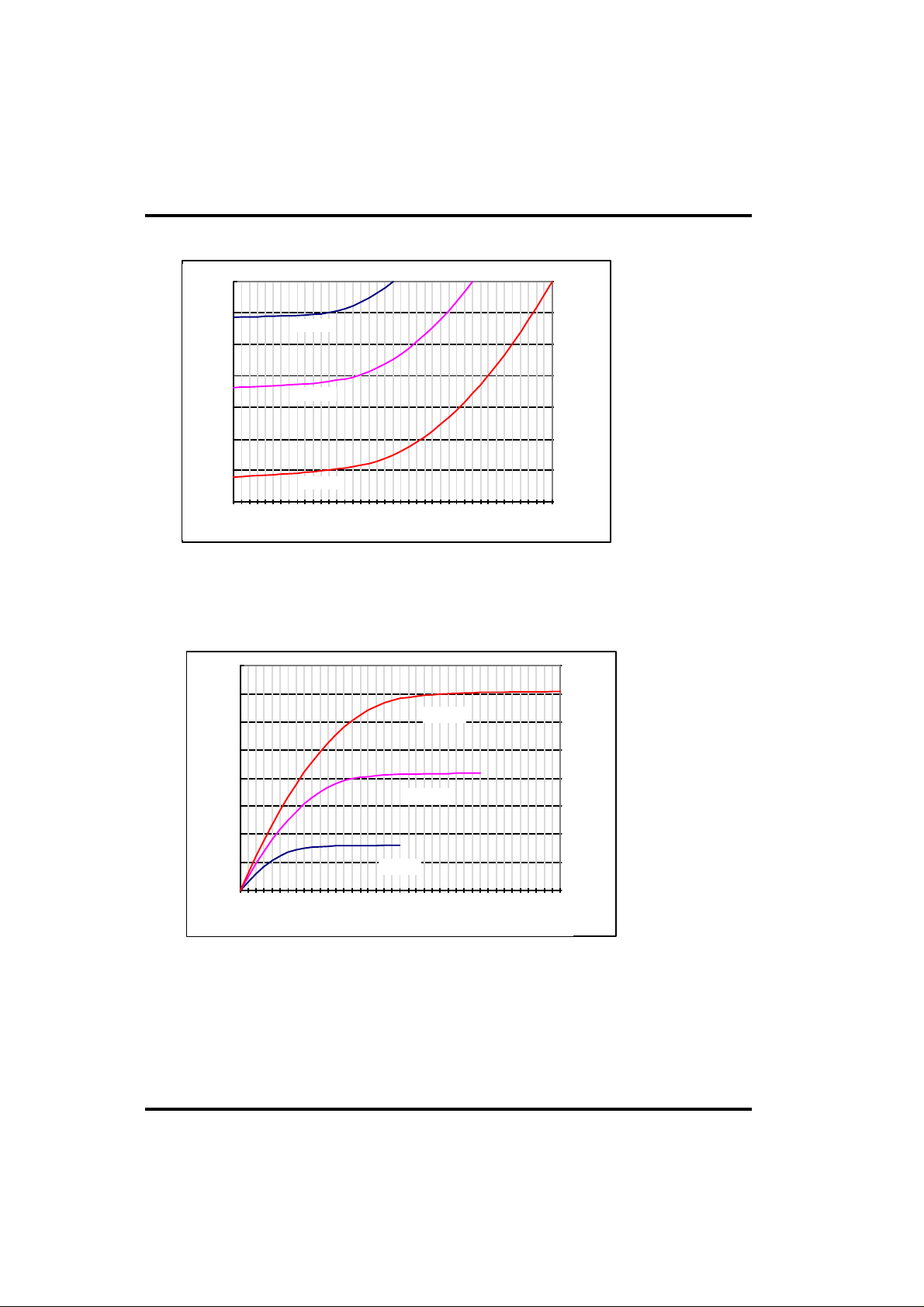
¡Ü GMS810 Series REMOUT port IOH Characteristics graph
0.0
-5.0
-10.0
-15.0
-20.0
IOH(mA)
-25.0
-30.0
-35.0
0 1 2 3 4
VDD=2V
VDD=3V
VDD=4V
VOH(V)
¡Ü GMS810 Series REMOUT port IOL Characteristics graph
8.00
7.00
6.00
5.00
VDD=4V
4.00
IOL(mA)
3.00
2.00
1.00
0.00
0 1 2 3 4
VDD=3V
VDD=2V
VOL(V)
1 - 15
Chapter 1. Overview
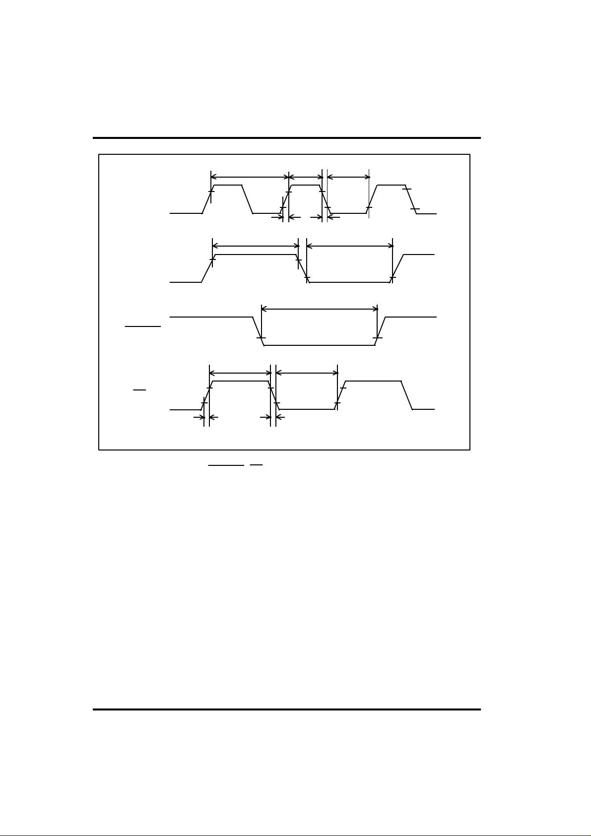
1.6.4 AC Characteristics (VDD = 2.0~4.0, Vss = 0V, Ta = 0¡É ~ 70¡É)
No Parameter Symbol UnitPin
External clock input cycle time
System clock cycle time
2
External clock pulse width High
3
External clock pulse width Low
4
External clock rising time
5
External clock falling time
6
interrupt pulse width High
7
Interrupt pulse width Low
8
Reset input pulse width low9
Event counter input pulse
10
width high
Event counter input pulse
11
width low
Event counter input pulse
12
rising time
Event counter input pulse
13
falling time
* Refer to Fig 1-1
tcp nsXin 250 500 10001
tsys
tcpH
tcpL
trcp
tfcp
tIH
tIL
tRSTL
tECH
tECL
trEC
tfEC
Xin
Xin
Xin
Xin
INT1~INT2
INT1~INT2
RESET
EC
EC
EC
EC
Specification
min typ max
500 1000 2000
40
40
40
40
2
2
8
2
2
40
40
ns
ns
ns
ns
ns
tsys
tsys
tsys
tsys
tsys
ns
ns
1 - 16
Chapter 1. Overview
Xin
INT1
INT2
RESET
EC
trCP
0.8Vcc
tfEC
tCPH
tfCP
tRSTL
tCP
tIH
tECH tECL
0.8Vcc 0.8Vcc
trEC
tCPL
Vcc-0.5V
0.5V
tIL
0.2Vcc
0.2Vcc
0.2Vcc
* FIG-1 : Clock, INT, RESET. EC input timing
1 - 17
OVERVIEW 1
FUNCTION DESCRIPTION 2
I/O PORT 3
PERIPHERAL HARDWARE 4
INTERRUPT 5
STANDBY FUNCTION 6
RESET FUNCTION 7
APPENDIX A. 8
APPENDIX B. 9
CHAPTER 2. FUNCTION DESCRIPTION
2.1 REGISTERS
15 7 0
Chapter 2. Function Description
PCH PCL
7 0
A
15 7 0
7 0
7 0
7 0
7 0
N V G B H I Z C
¡é
X
Y
SP
PSW
Program Counter
A-Register
YA (16bit Accumulator)
X-Register
Y-Register
Stack Pointer ¡Ø1
Program Status Word
¡é
Carry Flag
Zero Flag
Interrupt Enable Flag
Half Carry Flag
Break Flag
G Flag
Overflow Flag
Negative Flag
¡Ø
1 Stack Address
15 7 0
PCH PCL
¡é
Fixed as 01XXh (=RAM 1page)
¡é
SP
2 - 1

Chapter 2. Function Description
2.1.1 A register
- 8bit Accumulator.
- In the case of 16-bit operation, compose the lower 8-bit of A, upper 8bit in Y (16-bit
Accumulator)
- In the case of multiplication instruction, execute as a multiplier register. After
multiplication operation, the lower 8-bit of the result enters. (Y*A ¡æ YA)
- In the case of division instruction, execute as the lower 8-bit of dividend. After
division operation, quotient enters.
2.1.2 X register
- General-purpose 8-bit register
- In the case of index addressing mode within direct page(RAM area), execute as
index register.
- In the case of division instruction, execute as register.
2.1.3 Y register
- General-purpose 8-bit register
- In the case of index addressing mode, execute as index register
- In the case of 16-bit operation instruction, execute as the upper 8-bit of YA (16-bit
accumulator).
- In the case of multiplication instruction, execute as a multiplicand register. After
multiplication operation, the upper 8-bit of the result enters.
- In the case of division instruction, execute as the upper 8-bit of dividend. After
division operation, remains enters.
- Can be used as loop counter of conditional branch command. (e.g.DBNE Y, rel)
2.1.4 Stack Pointer
- In the cases of subroutine call, Interrupt and PUSH, POP, RETI, RET instruction,
stack data on RAM or in the case of returning, assign the storage location having
stacked data.
- Stack area is constrained within 1-page (00H-FFH). The SP is post-decremented
when a subroutine call or a push instruction is executed, or when an interrupt is
accepted; and the SP is pre-incremented when a return or a pop instruction is
executed.
- SP should be initialized as follows
ex) LDX #0FEH : 0FEH ¡æ X reg.
TXSP : X reg. ¡æ SP
- The behaviors of stack pointer according to each instruction are the following.
2 - 2
2.1.4.1 Interrupt
Chapter 2. Function Description
M(SP) ¡ç (PCH)
SP ¡ç SP - 1
2.1.4.2 RETI( Return from interrupt )
SP ¡ç SP + 1
(PSW) ¡ç M(SP)
2.1.4.3 Subroutine call
M(SP) ¡ç (PCH)
SP ¡ç SP - 1
M(SP) ¡ç (PCL)
SP ¡ç SP - 1
SP ¡ç SP + 1
(PCL) ¡ç M(SP)
M(SP) ¡ç (PCL)
SP ¡ç SP - 1
M(SP) ¡ç (PSW)
SP ¡ç SP - 1
SP ¡ç SP + 1
(PCH) ¡ç M(SP)
2.1.4.4 RET(Return from subroutine)
SP ¡ç SP + 1
(PCL) ¡ç M(SP)
SP ¡ç SP + 1
(PCH) ¡ç M(SP)
2 - 3
Chapter 2. Function Description
2.1.4.5 PUSH A(X, Y, PSW)
M(SP) ¡ç A
SP ¡ç SP - 1
2.1.4.6 POP A(X, Y, PSW)
SP ¡ç SP + 1
A ¡ç M(SP)
2.1.5 PC (Program Counter)
- Program counter is a 16-bit counter consisted of 8-bit register PCH and PCL.
- Addressing space is 64K bytes.
2.1.6 PSW (Program Status Word)
- PSW is an 8-bit register.
- Consisted of the flags showing the post state of operation and the flags determining
the CPU operation, initialized as 00H in reset state.
2.1.7 Flag register.
2.1.7.1 Carry flag (C)
- After operation, set when there is a carry from bit7 of ALU or there is not a borrow.
- Set by SETC and clear by CLRC.
- Executable as 1-bit accumulator.
- Branch condition flag of BCS, BCC.
2.1.7.2 Zero flag (Z)
- After operation also including 16-bit operatiion, set if the result is ¡È0
¡È
- Branch condition flag of BEQ, BNE.
2.1.7.3 Interrupt enable flag (I)
- Master enable flag of interrupt except for RST (reset).
- Set and cleared by EI, DI
2 - 4

Chapter 2. Function Description
2.1.7.4 Half carry flag (H)
- After operation, set when there is a carry from bit3 of ALU or there is not a borrow
from bit4 of ALU.
- Can not be set by any instruction.
- Cleared by CLRV instruction like V flag.
2.1.7.5 Break flag (B)
- Set by BRK (S/W interrupt) instruction to distinguish BRK and TCALL instruction
having the same vector address.
2.1.7.6 G flag (G)
- Set and cleared by SETG, CLRG instruction.
- Assign direct page (0-page, 1-page).
- Addressable directly to RAM 1-page by SETG. and to RAM 0-page by CLRG.
2.1.7.7 Overflow flag (V)
- After operation, set when overflow or underflow occurs.
- In the case of BIT instruction, bit6 memory location is transferred to V-flag.
- Cleared by CLRV instruction, but not set by any instruction.
- Branch condition flag of BVS, BVC.
2.1.7.8 Negative flag (N)
- Set whenever the result of a data transfer or operation is negative (bit7 is set to
¡È1¡È
).
- In the case of BIT instruction, bit7 of memory location is transferred to N-flag
- N-flag is not affected by CLR or SET instruction.
- Branch condition flag of BPL, BMI.
2 - 5
Chapter 2. Function Description
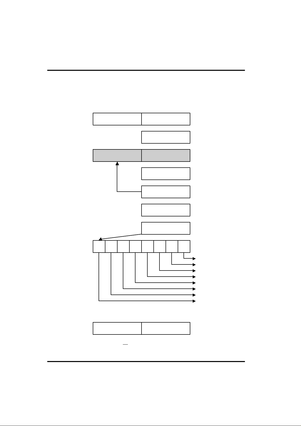
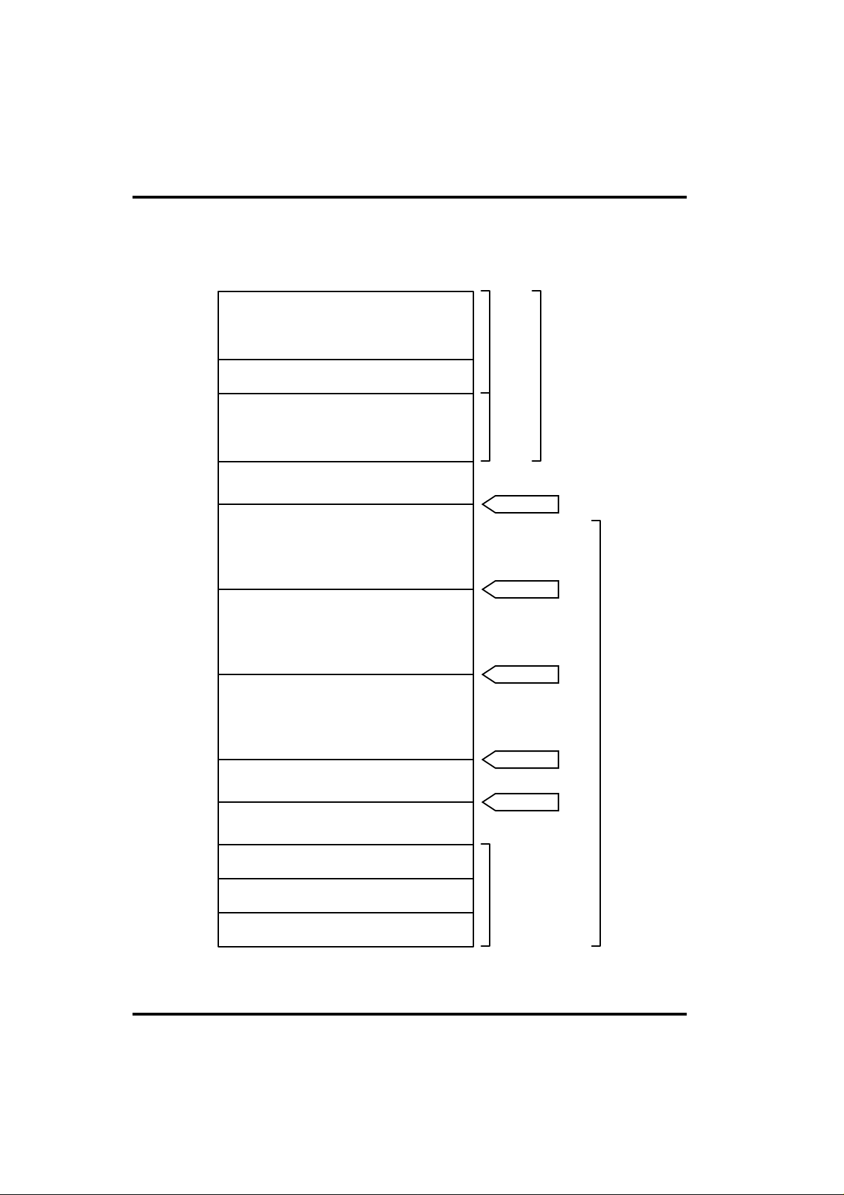
2.2 MEMORY MAP
0000h
RAM
(192 BYTES)
00BFh
PERIPHERAL REGISTERS
0100h
0-PAGE
DIRECT PAGE
0200h
8000h
A000h
C000h
E000h
F000h
FF00h
FFC0h
FFE0h
FFFFh
RAM (STACK)
(256 BYTES)
NON-USE
ROM
(32,768 BYTES)
ROM
(24,576 BYTES)
ROM
(16,384 BYTES)
ROM
(8,192 BYTES)
ROM
(4,096 BYTES)
PCALL AREA
TCALL VECTOR AREA
INTERRUPT VECTOR AREA
1-PAGE
GMS81032
GMS81024
GMS81016
PROGRAM ROM
GMS81008
GMS81004
U-PAGE
2 - 6
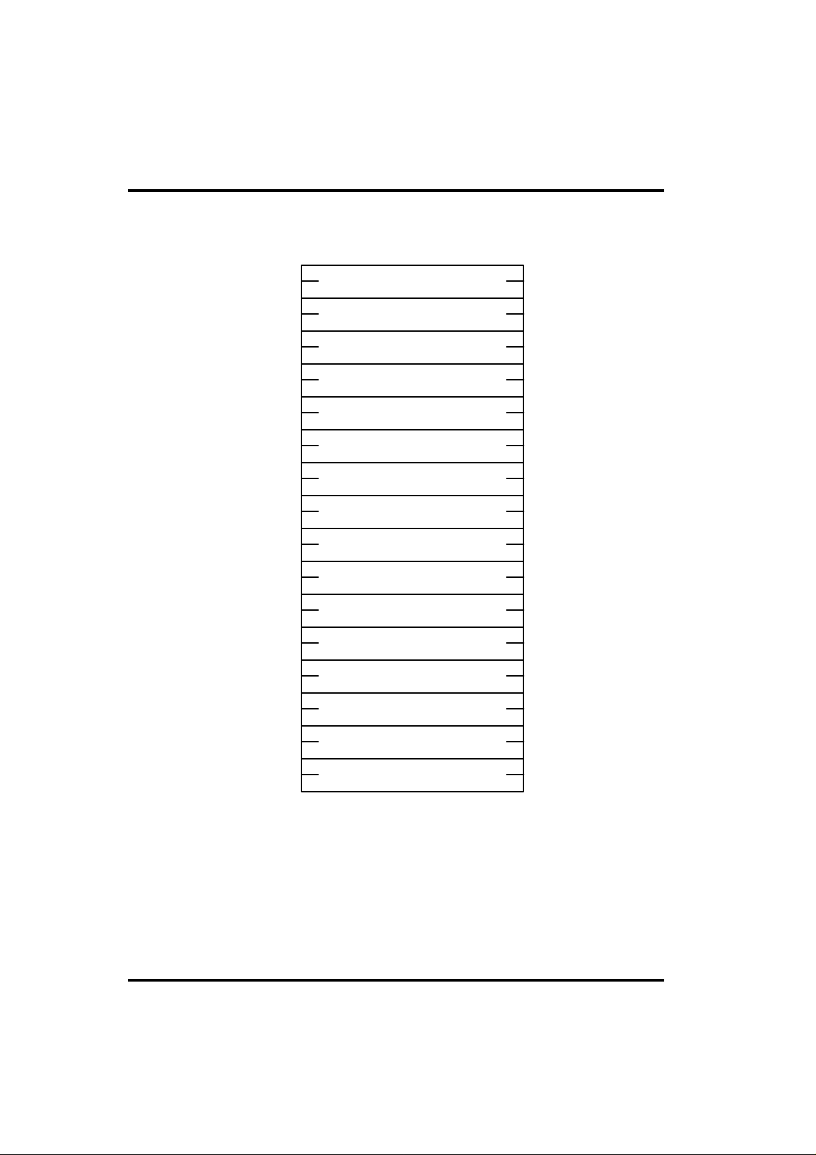
2.3 TCALL VECTOR AREA
Chapter 2. Function Description
FFC0h
FFC1h
FFC2h
FFC3h
FFC4h
FFC5h
FFC6h
FFC7h
FFC8h
FFC9h
FFCAh
FFCBh
FFCCh
FFCDh
FFCEh
FFCFh
FFD0h
FFD1h
FFD2h
FFD3h
FFD4h
FFD5h
FFD6h
FFD7h
FFD8h
FFD9h
FFDAh
FFDBh
FFDCh
FFDDh
FFDEh
FFDFh
TCALL 15
TCALL 14
TCALL 13
TCALL 12
TCALL 11
TCALL 10
TCALL 9
TCALL 8
TCALL 7
TCALL 6
TCALL 5
TCALL 4
TCALL 3
TCALL 2
TCALL 1
TCALL 0
(L)
(H)
(L)
(H)
(L)
(H)
(L)
(H)
(L)
(H)
(L)
(H)
(L)
(H)
(L)
(H)
(L)
(H)
(L)
(H)
(L)
(H)
(L)
(H)
(L)
(H)
(L)
(H)
(L)
(H)
(L)
(H)
*
* This vector area is used in BRK command and TCALL0 command.
2 - 7
 Loading...