

HEI GL6962A, GL6962 Datasheet
1
2 3
6 7
15
12 11 10 9
GL6962
Description
The GL6962 and GL6962A are bipolar integrated
circuits that perform all speech and line interface
functions required in fully electronic telephone sets.
They perform electronic switching between dialing
and speech. The ICs operate at line voltage down
to 1.6V DC (with reduced performance) to
facilitate the use of more telephone sets connected
in parallel.
Features
Low DC line voltage: operates down to 1.6V
(excluding polarity guard)
Voltage regulator with adjustable static
resistance
Provides a supply for external circuits
Symmetrical high-impedance inputs (64k¥Ø) for
dynamic, magnetic or piezo-electric microphones
Asymmetrical high-impedance inputs(32k¥Ø)
for electric microphones
DTMF signal input with confidence tone
MUTE input for pulse or DTMF dialing
(GL6962)
input for pulse or DTMF dialing
MUTE
(GL6962A)
Receiving amplifier for dynamic, magnetic or
piezo-electric earpieces.
Large gain setting ranges on microphone and
earpiece amplifiers.
Line loss compensation (line current dependent)
for microphone and earpiece amplifiers
Gain control curve adaptable to exchange supply
DC line voltage adjustment facility
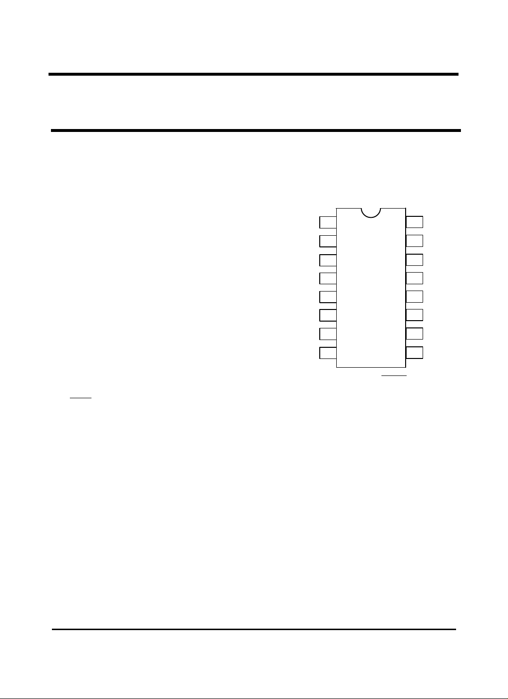
Packaged in 16 DIP/SOP.
GL6962/GL6962A
GL6962/GL6962A
Low Voltage Universal Speech Network
PIN Configuration
LN
TGA1
TGA2
QR
RGA
MIC-
MIC+
I
ref
* Pin 12 is active LOW(MUTE) for GL6962A
1
4
5
8
(TOP View)
16
14
13
SLPE
AGC
REG
V
CC
MUTE
DTMF
IR
VEE
2
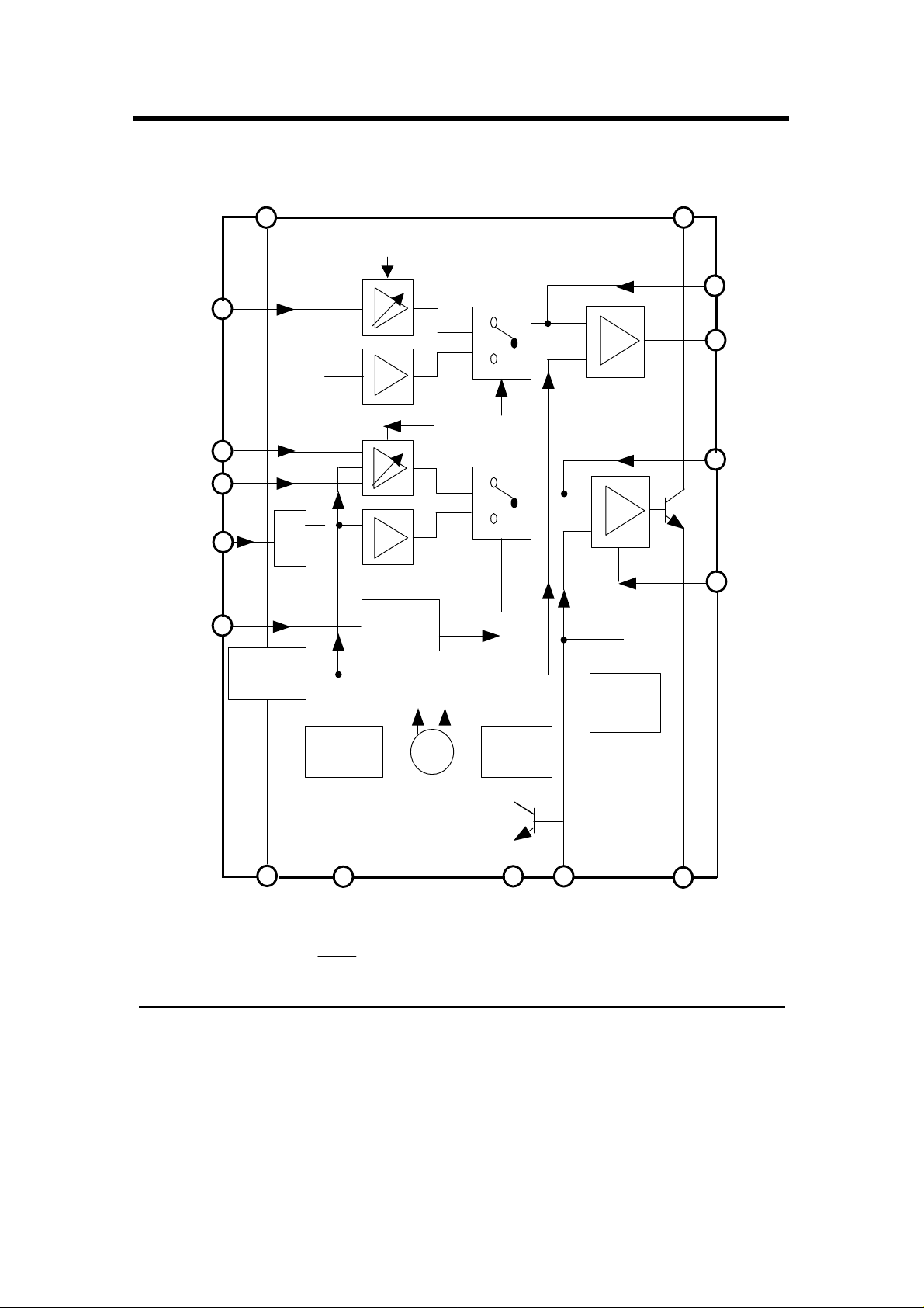
Block Diagram
8
14
15 9 16
1
4 2 3
10
7 6 11
12
5
13
CIRCUIT
+
+
DTMF
(1)
Ó
GL6962/GL6962A
IR
MIC
MIC-
MUTE
V
CC
dB
SUPPLY
&
+
+
MUTE
CONTROL
RGC TGC
RM
RM
-
-
LOW
VOLTAGE
LN
RGA
QR
TGA1
TGA2
VEE
* Pin 12 is active LOW (
CURRENT
REFERENCE
I
ref
) for GL6962A.
MUTE
CURRENT
CONTROL
REG AGC
SLPE
3
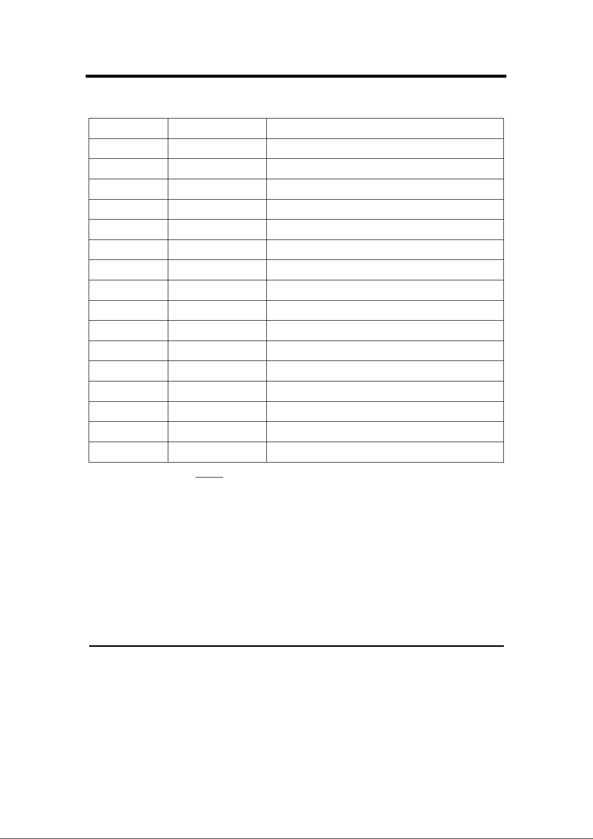
Pin Description
PIN NUMBER SYMBOL DESCRIPTION
1 LN Positive line terminal
2 TGA1 Gain adjustment: transmitting amplifier
3 TGA2 Gain adjustment: transmitting amplifier
4 QR Non-inverting output: receiving amplifier
5 RGA Gain adjustment: receiving amplifier
6 MIC- Inverting microphone input
7 MIC+ Non-Inverting microphone input
GL6962/GL6962A
8 I
Current stabilizer
ref
9 VEE Negative line terminal
10 IR Receiving amplifier input
11 DTMF Dual-tone multi-frequency input
12 MUTE Mute input
13 VCC Positive decoupling
14 REG Voltage regulator decoupling
15 AGC Automatic gain control input
16 SLPE Slope (DC resistance) adjustment.
(1) Pin 12 is active LOW (MUTE ) for GL6962A.
(1)
GL6962/GL6962A
4
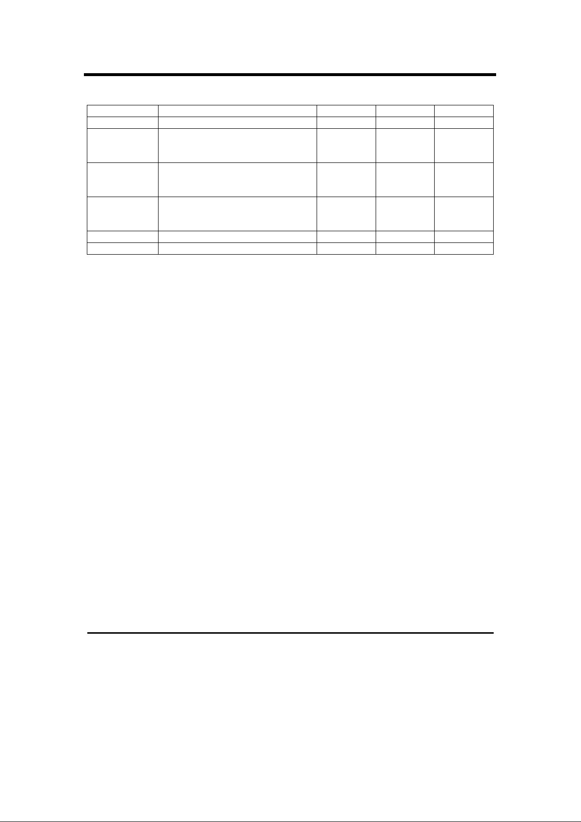
Absolute Maximum Ratings
SYMBOL PARAMETER MIN MAX UNIT
V
I
P
T
T
LN
line
V
i
tot
amb
stg
Positive continuous line voltage - 12 V
Line Current
R9 = 20 ; Note1
GL6962 ; GL6962A
Input voltage on all other pins
Positive input voltage
Negative input voltage
Total power dissipation
R9 = 20 ; Note2
GL6962 ; GL6962A
Operating ambient temperature -25 +75 ¡É
Storage temperature -40 +125 ¡É
-
-
-
-
140
VCC+0.7
-0.7
666
mA
V
V
mW
Maximum Ratings are those values beyond which damage to the device may occur.
Functional Operation should be restricted to the limits in the Electrical Characteristics tables or
pin Descriptions section
Notes to the Absolute Maximum Ratings
1. Mostly dependent on the maximum required T
2. Calculated for the maximum ambient temperature specified T
junction temperature of 125¡É.
and on the voltage between LN and SLPE.
amb
= 75¡É and maximum
amb
 Loading...