

HEI GL494 Datasheet
1
Q
+ + −
−
Description
The GL494 incorporates on a single monolithic chip all the
functions required in the construction of a pulse-widthmodulation control circuit. Designed primarily for power
supply control, the GL494 contains an on-chip 5-volt
regulator, two error amplifiers, adjustable oscillator, deadtime control comparator, pulse-steering flip-flop, and
output-control circuitry. The uncommitted output
transistors pro-vide either common-emitter or emitterfollower output capability. Push-pull or single-ended
output operation may be selected through the outputcontrol function. The ar-chitecture of the GL494 prohibits
the possibility of either output being pulsed twice during
push-pull operation.
Features
— Complete PWM Power Control Circuitry
— Uncommitted Outputs for 200mA Sink or Source
— Output Control Selects Single-Ended or Push-Pull
Operation
— Internal Circuitry Prohibits Double Pulse at Either
Output
— Internal Regulator Provides a Stable 5V Reference
Supply
— Variable Dead-Time Provides Control Over Total
Range
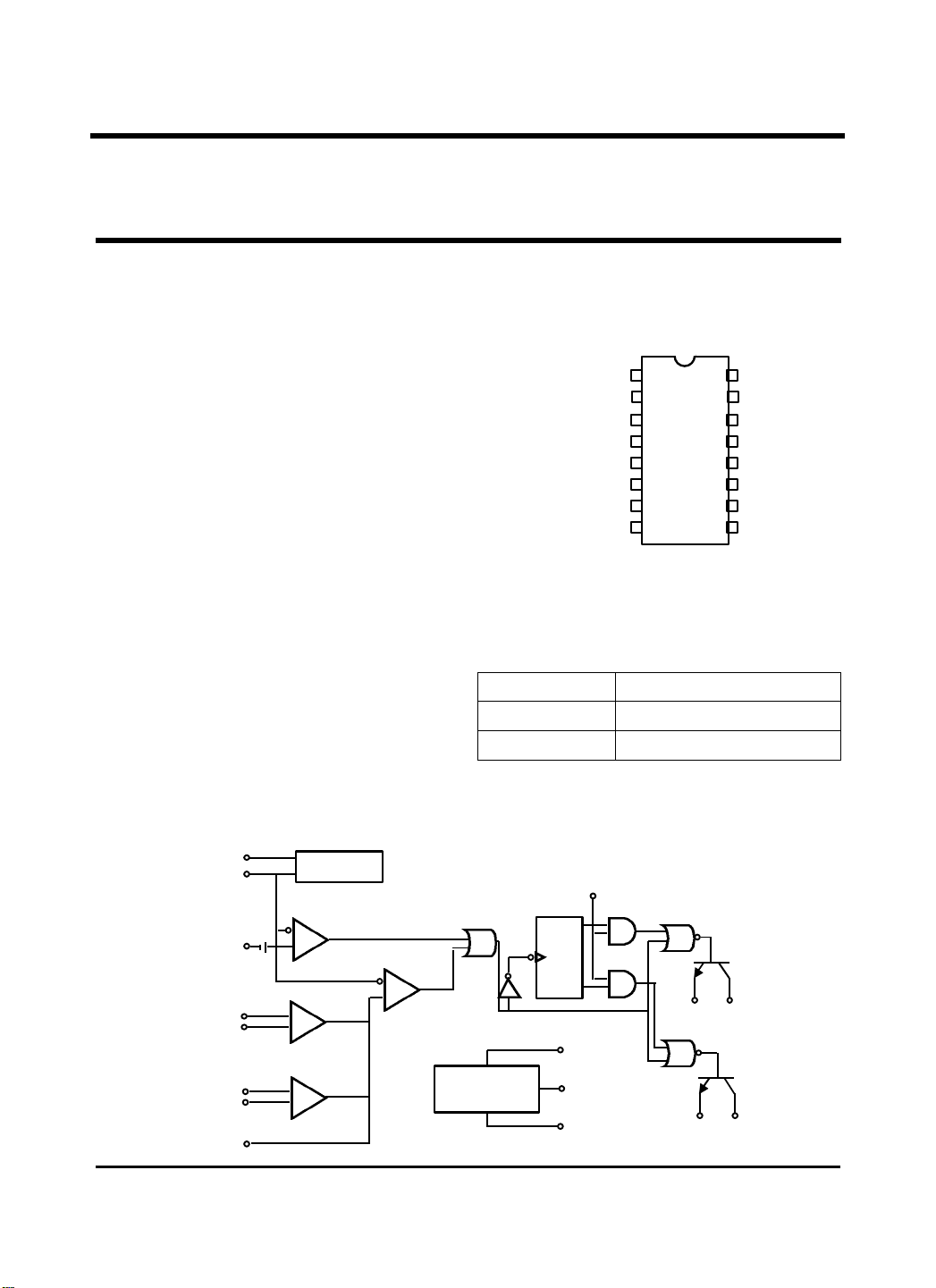
GL494
GL494
PWM CONTROL CIRCUIT
Pin Configuration
NONINV INPUT
INV. INPUT
FEEDBACK
DEAD TIME CONTROL
Cr
Rr
GND
C1
1
2
3
4
5
6
7
8
Function Table
Output Control Output Function
Grounded Single-ended or Parallel Output
At
V Normal Push-Pull Operation
ref
16
NON INV INPUT
15
INV. INPUT
14
REF. OUT
13
OUTPUT CONTROL
12
Vcc
11
C2
10
E2
9
E1
Block Diagram
DEAD
TIME
CONTROL
NONINVERTING(1)
INPUT
INVERTING (2)
INPUT
NONINVERTING(16)
INPUT
INVERTING (15)
INPUT
FEEDBACK
RT
CT
OSCILLATOR
0.1V
(4)
ERROR AMPLIFIERS
ERROR AMP1
ERROR AMP2
(3)
PWM
COMPARATOR
REFERENCE
REGULATOR
PULSE STEERING
(See Function Table)
FLIP FLOP
T
OUTPUT
CONTROL
(13)
Q
VCC
(12)
REF OUT
(14)
GND
(7)
E1(9) C1(8)
E1(10) C2(11)
2
Absolute Maximum Ratings
°
°
K
°
°
−
=
=
°
=
=
°
=
°−=
°
=
µ
=,Ω
=
=
°
=
µ
=,Ω
=
°−=
Supply Voltage,
Amplifier Input Voltage ………………………………………………………………..
Collector Output Voltage ……………………………………………………………………… 41 V
Continuous Total dissipation at (or below) 25C° ………………………………………. 1000 mW
Operating Free-Air Temperature Range ……………………………………………… -20 to 85
Storage Temperature Range ……………………………………………………….….. -65 to 150
Collector Output Current ………………………………………………………………….. 250 mA
V ……………………………………………………………………….. 41 V
CC
V +0.3 V
CC
Recommended Operation Conditions
PARAMETER MIN MAX UNIT
Supply Voltage,
Amplifier Input Voltage,
V 7 40 V
CC
V -0.3
1
V -2 V
CC
Collector Output Voltage, Vo 40 V
Collector Output Current
200 mA
(Each Transistor)
Current Into Feed back Terminal 0.3 mA
Timing Capacitor,
Timing Resistor,
C 0.47 10,000 nF
T
R 1.8 500 Ω
T
Oscillator Frequency 1 300 KHz
Operating Free-Air Temperature -20 85
Electrical Characteristics (Temperature
,
V =15V, f=10KHz)
C85~20
CC
Reference Section
PARAMETER TEST CONDITIONS MIN TYP(1) MAX UNIT
Output voltage (
Input regulation V7V
Output regulation 1I
Output Voltage change
with temperature
Short-circuit
Output current(2)
V ) mA1I
ref
O
CC
O
A
ref
4.75 5 5.25 V
to 40V, C25T
to 10mA, C25T
C20T
to
0V
35 mA
A
A
0.2 1 %
C85
2 25 mV
1 15 mV
GL494
C
C
C
Oscillator Section
PARAMETER TEST CONDITIONS MIN TYP(1) MAX UNIT
Frequency F01.0C
Standard deviation
of frequency (3)
Frequency change with
Voltage
Frequency change with
temperature
T
All values of
T,R,C Constant
ATT
V7V
CC
T
A
to 40V, C25T
F01.0C
C20T
to
T
V ,
CC
T
C85°
k12R
10 KHz
10 %
A
k12R
0.1 %
2 %
3
Dead Time Control Section
°
=
GL494
PARAMETER TEST CONDITIONS MIN TYP(1) MAX UNIT
Input bias current (pin 4) VI=0 to 5.25V -2 -10 Aµ
Maximum duty cycle,
Each output
Input threshold voltage
(pin 4)
V =0V 45 %
)4pin(I
Zero duty cycle 3 3.3 V
Maximum duty cycle 0 V
Error Amp Sections
Input offset voltage V5.2V
Input offset current V5.2V
Input bias current V5.2V
Common-mode input
voltage range
Open-loop voltage
Amplification
Unity-gain bandwidth 800 KHz
Common-mode rejection ratio
Output sink current (pin 3)
Output source current (pin 3)
PARAMETER TEST CONDITIONS MIN TYP(1) MAX UNIT
= 2 10 mV
)3PIN(O
= 25 250 nA
)3PIN(O
= 0.2 1 Aµ
)3PIN(O
5V
−= to –5V,
ID
V7VCC=
to 40V
==∆ to3.
OO
V40VCC= , C25T
A
mV15V
V7.0V
=
)3pin(O
mV15VID= to 5V,
V5.3V
=
)3pin(O
LOW
HIGH
5.0V,V3V
-0.3
2VCC−
70 95 dB
65 80 dB
0.3 0.7 mA
-2 mA
V
PWM Comparaor Section
Input threshold voltage (pin 3) Zero duty cycle 4 4.5 V
Input sink current (pin 3) V7.0V
PARAMETER TEST CONDITIONS MIN TYP(1) MAX UNIT
= 0.3 0.7 mA
)3pin(O
Switching Characteristics
PARAMETER TEST CONDITIONS MIN TYP(1) MAX UNIT
Output Voltage rise time 100 200 ns
Output Voltage fall time
Output Voltage rise time 100 200 ns
Output Voltage fall time
Common-emitter configuration,
See Test Circuit 3
Emitter-follower configuration,
See Test Circuit 4
25 100 ns
40 100 ns
 Loading...