


GDC21D601
32-Bit RISC MCU
Ver 1.6
HDS-GDC21D601-9908 / 10

GDC21D601
The information contained herein is subject to change without notice.
The information contained herein is presented only as a guide for the applications of our products. No
responsibility is assumed by Hyundai for any infringements of patents or other rights of the third parties
which may result from its use. No license is granted by implication or otherwise under any patent or
patent rights of Hyundai or others.
These Hyundai products are intended for usage in general electronic equipment (office equipment,
communication equipment, measuring equipment, domestic electrification, etc.).
Please make sure that you consult with us before you use these Hyundai products in equipment which
require high quality and / or reliability, and in equipment which could have major impact to the welfare of
human life (atomic energy control, airplane, spaceship, traffic signal, combustion control, all types of
safety devices, etc.). Hyundai cannot accept liability to any damage which may occur in case these
Hyundai products were used in the mentioned equipment without prior consultation with Hyundai.
Copyright 1999 Hyundai Micro Electronics Co.,Ltd.
All Rights Reserved
3

GDC21D601
TABLE OF CONTENTS
Section 1. Overview.....................................................................................................................8
1. General Description..............................................................................................................8
2. Feature................................................................................................................................10
3. Package..............................................................................................................................12
4. Pin Assignment...................................................................................................................13
5. Pin Descriptions..................................................................................................................15
Section 2. System Architecture ................................................................................................20
1. Internal Bus Architecture.....................................................................................................20
2. Arbiter .................................................................................................................................20
3. System Decoder .................................................................................................................21
4. Memory Map.......................................................................................................................21
5. Memory Format...................................................................................................................22
6. Boot Mode...........................................................................................................................22
7. Multi-Function Pin ...............................................................................................................23
Section 3. ARM720T Core..........................................................................................................24
1. General Description............................................................................................................24
2. Feature................................................................................................................................24
3. Core Block Diagram............................................................................................................26
Section 4. DRAM Controller......................................................................................................27
1. General Description............................................................................................................27
2. Hardware Interface and Signal Description ........................................................................28
3. Functional Description ........................................................................................................31
4. Register Description............................................................................................................34
Section 5. On-Chip SRAM .........................................................................................................37
1. General Description............................................................................................................37
2. Signal Description...............................................................................................................37
3. Function Description...........................................................................................................37
Section 6. Static Memory Controller........................................................................................38
1. General Description............................................................................................................38
2. Signal Description...............................................................................................................39
3. Functional Description ........................................................................................................43
4. Programmer’ s Model..........................................................................................................45
4

GDC21D601
Section 7. MCU Controller.........................................................................................................48
1. General Description............................................................................................................48
2. Signal Description...............................................................................................................48
3. Register Description............................................................................................................49
Section 8. Power Management Unit.........................................................................................54
1. General Description............................................................................................................54
2. Hardware Interface and Signal Description ........................................................................55
3. Operation Modes ................................................................................................................56
4. Register Description............................................................................................................58
5. Power Management Unit Register Map..............................................................................63
6. Test Mode Guide for MCU..................................................................................................64
7. Signal Timing Diagram........................................................................................................66
Section 9. Watchdog Timer.......................................................................................................68
1. General Description............................................................................................................68
2. Hardware Interface and Signal Description ........................................................................69
3. Watchdog Timer Introduction .............................................................................................71
4. Watchdog Timer Operation ................................................................................................72
5. Watchdog Timer Memory Map ...........................................................................................74
6. Watchdog Timer Register Descriptions..............................................................................75
7. Examples of Register Setting..............................................................................................77
Section 10. Interrupt Controller................................................................................................81
1. General Description............................................................................................................81
2. Hardware Interface and Signal Description ........................................................................82
3. Interrupt Controller..............................................................................................................84
4. Interrupt Controller Memory Map........................................................................................86
5. Interrupt Controller Register Descriptions...........................................................................87
Section 11. Real Time Clock .....................................................................................................91
1. General Description............................................................................................................91
2. Signal Description...............................................................................................................92
3. Hardware Interface .............................................................................................................93
4. Functional Description ........................................................................................................94
5. Real Time Clock Memory Map ...........................................................................................95
6. Real Time Clock Register Descriptions..............................................................................95
5

GDC21D601
Section 12. General Purpose Timer Unit .................................................................................96
1. General Description............................................................................................................96
2. Hardware Interface and Signal Description ........................................................................97
3. General Purpose Timer Unit Introduction.........................................................................100
4. General Purpose Timer Unit Operation............................................................................101
5. General Purpose Timer Unit Memory Map.......................................................................102
6. General Purpose Timer Unit Register Descriptions..........................................................104
7. Examples of Register Setting............................................................................................108
Section 13. PIO.........................................................................................................................111
1. General Description..........................................................................................................111
2. Signal Description.............................................................................................................112
3. Hardware Interface ...........................................................................................................115
4. Functional Description ......................................................................................................116
5. Programmer’ s Model........................................................................................................117
Section 14. Synchronous Serial Peripheral Interface...........................................................118
1. General Description..........................................................................................................118
2. Signal Description.............................................................................................................119
3. Hardware Interface ...........................................................................................................120
4. Functional Description ......................................................................................................121
5. Register Memory Map.......................................................................................................123
6. SSPI Data Clock Timing Diagram.....................................................................................124
Section 15. UART.....................................................................................................................125
1. General Description..........................................................................................................125
2. Features............................................................................................................................125
3. Signal Description.............................................................................................................126
4. Internal Block Diagram......................................................................................................129
5. Registers Description........................................................................................................130
Section 16. Smart Card Interface............................................................................................142
1. General Description..........................................................................................................142
2. Signal Description.............................................................................................................143
3. Hardware Interface ...........................................................................................................144
4. Functional Description ......................................................................................................145
5. Programmer’ s Model........................................................................................................146
6

GDC21D601
Section 17. I2C Controller........................................................................................................149
1. General Description..........................................................................................................149
2. I2C Controller Key Features..............................................................................................150
3. I2C Controller Clocking and Pin Functions........................................................................150
4. I2C Master Mode Transmit / Receive Process..................................................................150
5. I2C Restart Capability (Combined Mode)..........................................................................151
6. I2C Controller Programming Model...................................................................................152
7. I2C Module Signal Description ..........................................................................................154
8. Hardware Interface ...........................................................................................................155
9. Register Memory Map.......................................................................................................156
Section 18. Direct Memory Access Controller ......................................................................157
1. General Description..........................................................................................................157
2. Signal Description.............................................................................................................158
3. Programmer’ s Model........................................................................................................159
4. Address Modes.................................................................................................................163
Section 19. Debug and Test Interface....................................................................................167
1. General Description..........................................................................................................167
2. Software Development Debug and Test Interface............................................................167
3. Test Access Port and Boundary Scan..............................................................................167
Section 20. Electrical Ratings.................................................................................................169
1. Absolute Maximum Ratings..............................................................................................169
2. Thermal Characteristics....................................................................................................169
3. D.C Electrical Characteristics ...........................................................................................169
APENDIX A. Register Map.......................................................................................................170
7
GDC21D601
GDC21D601
32-Bit RISC MCU
Section 1. Overview
1. General Description
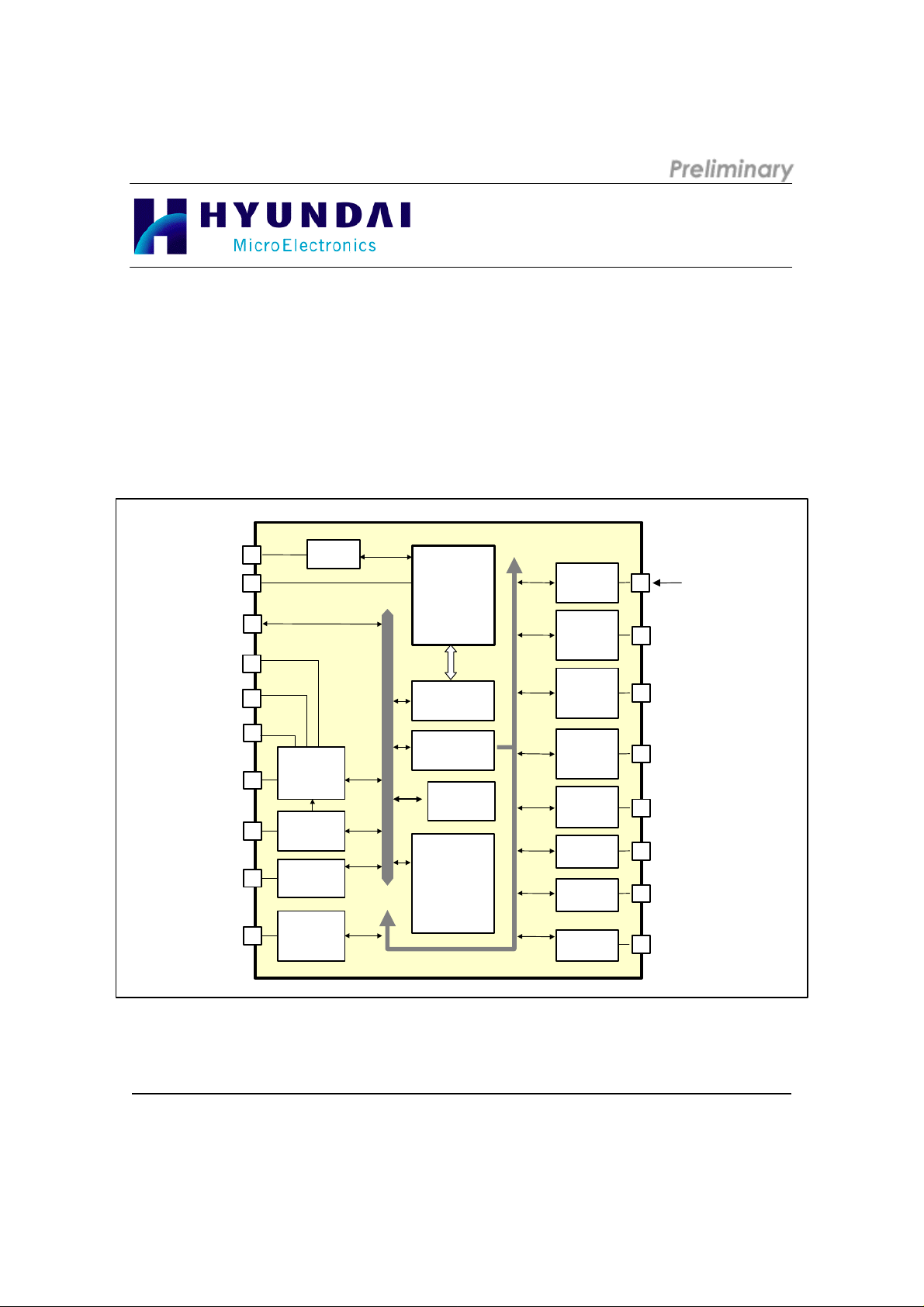
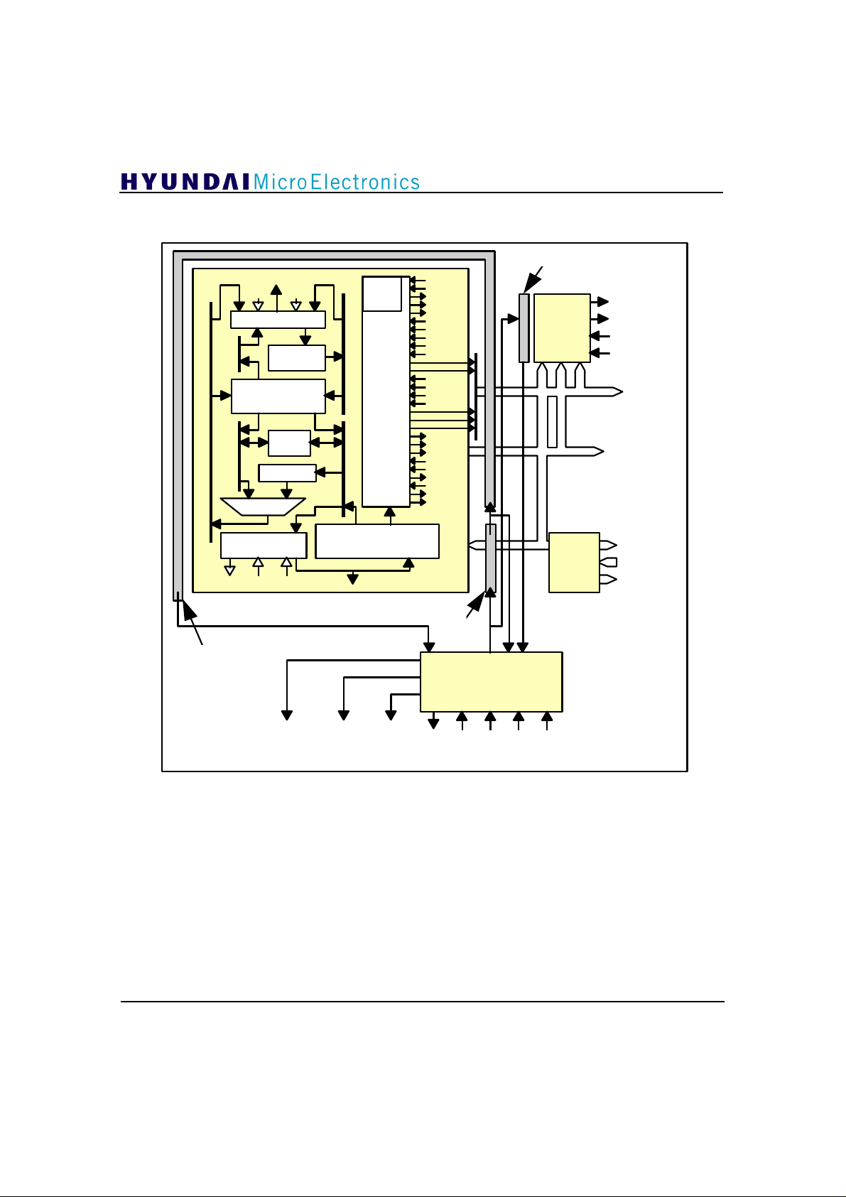
The GDC21D601 is the HME’s 32bit high performance microcontroller unit (MCU). The GDC21D601 contains
ARM720T, which is a general-purpose 32bit microprocessor, and extensive peripherals: 6 channel 16bit Timer,
Watch Dog Timer, 2 channel UART, 2 channel SSPI, 3 channel I2C, Programmable Priority Interrupt Controller,
10 port PIO, 2 channel DMA Controller, External Memory Controller and BUS Controller including chip select
logic.
ARM720T is a 32bit Microprocessor with the CPU of the ARM7TDMI, 8KB Cache, enlarged write buffer and
Memory Management Unit (MMU). The ARM720T is fully software compatible with the ARM processor family.
JTAG[0:4]
RESET
EXPRDY
EXPCLK
Mode[0:2]
DRAM OE, WE
WR[0:3], RD
RD&WR
BCLKOUT / PORT F[5]
BWAIT / PORT F[4]
A[0:31]
D[0:31]
nCS[4:7] / PORT H[4:7]
RAS[0:1] / PORT G[6:7]
CAS[0:3] / PORT G[0:3]
DREQ[0:1] / PORT G[2:3]
DACK[0:1] / PORT G[4:5]
IRQ[0:5] / PORT A[0:5]
nCS[0:3]
Bus
controller
DRAM
controller
DMA
controller
INT
controller
JTAG
ASB
APB
32-bit
ARM 720T
Core
AMBA Logic
APB Bridge
MCU
controller
Internal
SRAM
(8KB)
GDC21D601
RTC
Timer
UART
I2C
controller
SSPI
PIO
PMU
WDT
RTCin/Out (32.768kHz)
PORT B[0:7] / Timer TCIO / PWM
PORT C[0:3] / Timer TCIO / PWM
TCLK A,B,C / PORT C[4:6]
UART channel 0 , 1
SMART Card / UART channel 2
( PORT D[0:7] ,PORT E[0:4] )
I2C channel 0
I2C channel 1
I2C channel 2
SSPI 0, 1
( PORT E[5:7], PORT F[0:4] )
PORT I[0:7]
PORTJ[0:7]
NPDM
WDTOUT
Figure. 1 GDC21D601 Block Diagram
8

GDC21D601
The general descriptions of the GDC21D601 like following :
• On-Chip Modular Architecture (using AMBA)
• Utilizes the ARM720T(“ARM7TDMI with 8Kbyte Cache and MMU”) 32bit RISC Family
• 8Kbyte internal SRAM
• support 8bit/16bit/32bit external Data bus width
• Eight Programmable Chip Select Outputs with EXPRDY
• Support Little and Big Endian memory format
• Low Power Consumption using Power Management Unit
• Fully static operation : Max. 80MHz
• Two 32bit DMA Controllers (External request only)
• Programmable Priority Interrupt Controller (6 external sources)
• Two DRAM Banks Support
• Six 16bit Multi Function Timers / Counters for General Purpose Applications
• One 8bit Watch Dog Timer (WDT)
• Real Time Clock : 32.768 KHz
• Three UARTs (Universal Asynchronous Receiver Transmitter) compatible with 16C550 UART, one
UART with Smart card interface
• Two SSPIs (Synchronous Serial Peripheral Interface) with FIFO
• Three I2C Master/Slave Controllers
• Programmable Input/Output (8bit 10 channel)
• 208 MQFP Package
9

2. Feature
GDC21D601
• ARM720T Core
- This is an ARM7TDMI CPU core with
. 8KB cache
. enlarged write buffer
. MMU(Memory Management Unit)
. On-chip ICEbreaker debug support
. 32-bit x 8 hardware multiplier
. Thumb decompressor
. High-performance 32-bit RISC architecture
. High-density 16-bit insturction set
Enhanced ARM software toolkit
THUMB code is able to provide up to 65% of
the code size of ARM, and 160% of the
performance of an equivalent ARM processor
connected to a 16-bit memory system.
The MMU supports 4G bytes Virtual address.
The allocation of virtual addresses with
different task ID improves performance in task
switching operations with the cache enabled.
• DMA Controller
- Two Channels with identical function
- Four Gigabytes of address space
- 256 Kbytes transfers to the maximum
- Data Transfer unit : Byte, Half-word, Word
- Two kinds of Bus mode
. Burst mode
. Exception mode(Cycle steal)
- Two kinds of address mode
. Single address mode
. Dual address mode
- Two types of Transfer request source
. External I/O request
. Auto-request
- Two kind of fixed priority for channels
- Interrupted when the data transfers are
complete
• DRAM Controller
- DRAM access
- Support Word, Half-word, and Byte transaction
- CBR refresh in normal operation and self-refresh
in power-down mode
- Support programmable refresh rate
- Support various DRAM access time by setting
the wait count control register
• Static Memory Controller
- Chip Select up to 8 (Each Bank is 256 MByte)
- Exchangeable Chip Select Active High/Low
(CS6 and CS7 only)
- Little-Endian and Big-Endian Memory Support
- Programmable wait-state (up to 16 wait-state)
- Support External BUS Ready Strobe
- Support various type Bus Control timing
- Support Word, Half-word, and Byte transaction
• On-Chip SRAM
- 8k Bytes(2048x32)
- Asynchronous SRAM
- Can write 8/16/32bits data, and read 32bits data
• MCU Controller
- The Memory Map Structure Control signals
- DRAM Power-Down Request and Powr-Down
Ack signal
- Generate the Multi Function Pin control signals
- Device Code : $GDC601
• Power Management Unit
- Power On Reset, WD_OF Reset, and S/W Reset
- Status : RESET, Power Down, RUN_FAST,
RUN_SLOW
- Provide separated clock for each modules on
chip
- Provide BCLKOUT, WD_OF, Power-Down pins
for external devices
• Watch Dog Timer
- Watchdog timer mode & interval timer mode
- Eight counter clock sources
- Generate the Power Down reset or the Watch
Dog Overflow
• Interrupt Controller
- Asynchronous interrupt controller
- Six external interrupt
- Twenty internal interrupt
- Level or edge triggered
- Mask for each interrupt source
Request of IRQ, FIQ for each interrupt source
10

GDC21D601
• Real Time Clock
- 32bit counter clocked by a 32.768KHz clock.
- 32bit match register
• Programmable Input Output
- up to 80 pin (8bit 10channel)
- Each pin can be configurable as either input or
output
• Timer
- 6 channel 16-bit up-count
- 4-internal pre-scaleable , 4-external input clock
. 1 interrupt per 1 channel
. 2 inout pin per 1 channel for input capture or
output compare
- Basic function :
. Compare match waveform output
. Input capture
. Match clear
. Capture clear
- Synchronous mode
. Synch. clear at two or more channel
. Synch. write at two or more channel
- PWM waveform output mode
• Synchronous Serial Interface
- Supports full duplex communication
- Sends and receives data continuously, using 16 x
8 bit FIFOs
- Built-in baud rate generator capable of
generation 4 clock rate
- Selectable clock source : either built-in buad-rate
generator or external clock
- 4 independent interrupts : transmit-end, rx-full,
tx-empty and tx-full
• UART
- 2 channel : UART only
. Compatible with 16550
. 16 byte each FIFO for TX / RX
. Start, stop and parity bit can be added or
deleted from/to serial data
. MODEM control functions (CTS, RTS, DSR,
DTR, RI and DCD )
. Fully programmable serial-interface
characteristics
: 5-, 6-, 7- or 8-bit characters
: even, odd or no-parity bit generation and
detection
: 1-, 1.5- or 2-stop bit generation and
detection
• SmartCard Interface
- 1 channel : Support SmartCard Interface
. Supports only asynchronous operation
. Supports cards that have internal reset
capability
. Supports cards that have an active low reset
input
. Supports cards that use the internal clock
. Generate the clock for a card expecting the
external clock
. Use the serial in/out ports for I/O
. Use the PIO ports for other interface signals
like RST, DETECT, etc
• I2C
- 3 channels
- Master / Slave function
- Programmable clock speed
- 8bit data transfer
- Slave clock stretch support
- Maskable interrupt
- Support clock rates up to 1.84MHz Baud
11
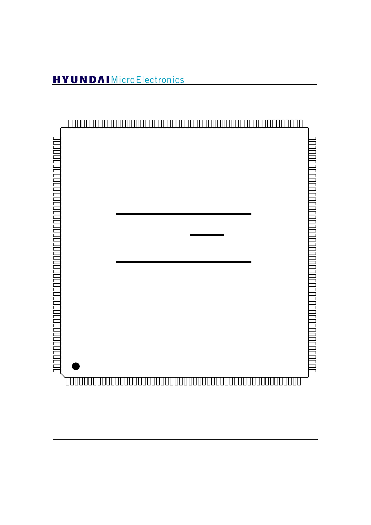
3. Package
9921
Rev. ES
12345678910111213141516171819202122232425262728293031323334353637383940414243
44
132
131
130
129
128
127
126
125
124
123
122
121
120
119
118
117
116
115
114
113
112
111
110
109
108
107
106
105
135
153
152
151
150
149
148
147
146
145
144
143
142
141
140
139
138
137
136
134
45464748495051
52
156
155
154
HME
32bit MCU
GDC21D601
157
158
159
160
161
162
163
164
165
166
167
168
169
170
171
172
173
174
175
176
177
178
179
180
181
182
183
184
185
186
187
188
189
190
191
192
193
194
195
196
197
198
199
200
201
202
203
204
205
206
207
208
ARM
GDC21D601R1
(Top View)
104
103
102
101
100
99
98
97
96
95
94
93
92
91
90
89
88
87
86
85
84
83
82
81
80
79
78
77
76
75
74
73
72
71
70
69
68
67
66
65
64
63
62
61
60
59
58
57
56
55
54
53
12
Figure 2. Package Outline
GDC21D601
4. Pin Assignment
PIN NAME PIN NAME PIN NAME PIN NAME
1 A0 45 IRQ0/PA0 89 VDD 133 NRAS0/PG6
2 A1 46 VDD 90 SMDI/PE2 134 VSS
3 VDD 47 IRQ1/PA1 91 SMDO/PE3 135 NRAS1/PG7
4 A2 48 IRQ2/PA2 92 SMCLK/PE4 136 NCAS0/PH0
5 A3 49 IRQ3/PA3 93 VSS 137 NCAS1/PH1
6 A4 50 VSS 94 SIN0/ PE5 138 NCAS2/PH2
7 VSS 51 IRQ4/PA4 95
8 A5 52 IRQ5/PA5 96 SCLK0/PE7 140 VSS
9 A6 53 PA6 97 VDD 141 XOUT
10 A7 54 PA7 98
11 VDD 55 TCIOA0/PB0 99
12 A8 56 VDD 100
13 A9 57 TCIOB0/PB1 101 VSS 145 NDRAMWE
14 A10 58 TCIOA1/PB2 102
15 VSS 59 TCIOB1/PB3 103 SCS1/PF4 147 NWR0
16 A11 60 VSS 104 BCLKOUT/PF5 148 NWR1
17 A12 61 TCIOA2/PB4 105 NFIQOUT/PF6 149 NWR2
18 VDD 62 TCIOB2/PB5 106 NIRQOUT/PF7 150 VDD
19 A13 63 TCIOA3/PB6 107 VDD 151 NWR3
20 A14 64 VDD 108 I2CSDA0 152 NRD
21 A15 65 TCIOB3/PB7 109 I2CSCL0 153 RDNWR
22 VSS 66 PC0/TCIOA4 110 I2CSDA1 154 VSS
23 A16 67 PC1/TCIOB4 111 VSS 155 NEXPRDY
24 A17 68 VSS 112 I2CSCL1 156 EXPCLK
25 A18 69 PC2/TCIOA5 113 I2CSDA2 157 NCS0
26 VDD 70 PC3/TCIOB5 114 I2CSCL2 158 NCS1
27 A19 71 PC4/TCLKA 115 VDD 159 NCS2
28 A20 72 VDD 116 Mode0/TREQA 160 VDD
29 A21 73 PC5/TCLKB 117 Mode1/TREQB 161 NCS3
30 VSS 74 PC6/TCLKC 118 Mode2/TACK 162 NCS4/PH4
31 A22 75 PC7/TCLKD 119 VSS 163 NCS5/PH5
32 A23 76 RXD0/PD0 120 UCLKOUT 164 VSS
33 WDTOUT 77 VSS 121 UCLKIN 165 CS6/PH6
34 NPDN 78 TXD0/PD1 122 VDD 166 CS7/PH7
35 VSS 79 RXD1/ PD2 123 TEST 167 D31/PJ7
36 RTCOSCIN 80 TXD1/PD3 124 NEXTREQ/PG0 168 VDD
37 RTCOSCOUT 81 VDD 125 NRESET 169 D30/PJ6
38 VDD 82 NCTS/ PD4 126 VSS 170 D29/PJ5
39 NTRST 83 NDSR/ PD5 127 NEXTACK/PG1 171 D28/PJ4
40 TDI 84 NDCD/ PD6 128 NDREQ0/PG2 172 VSS
41 TCK 85 VSS 129 NDACK0/PG3 173 D27/PJ3
42 VSS 86 NRI/ PD7 130 VDD 174 D26/PJ2
43 TDO 87 NDTR/PE0 131 NDREQ1/PG4 175 D25/PJ1
44 TMS 88 NRTS/PE1 132 NDACK1/PG5 176 VDD
SOUT0/PE6
SCS0/PF0/MemByte0
SIN1/PF1/MemByte1
SOUT1/PF2
SCLK1/PF3
139 NCAS3/PH3
142 XIN
143 VDD
144 NDRAMOE
146 VSS
13
GDC21D601
PIN NAME PIN NAME PIN NAME PIN NAME
177 D24/PJ0 185 VDD 193 VDD 201 VDD
178 D23/PI7 186 D17/PI1 194 D11 202 D5
179 D22/PI6 187 D16/PI0 195 D10 203 D4
180 D21/PI5 188 D15 196 D9 204 D3
181 VSS 189 VSS 197 VSS 205 VSS
182 D20/PI4 190 D14 198 D8 206 D2
183 D19/PI3 191 D13 199 D7 207 D1
184 D18/PI2 192 D12 200 D6 208 D0
14
5. Pin Descriptions
PIN NUMBER PIN NAME TYPE DESCRIPTION
1~2, 4~6, 8~10,
12~14, 16~17,
19~21, 23~25,
27~29, 31~32
33 WDTOUT O Watch Dog Timer Overflow Output
34 NPDN O Power Down Signal from PMU block
37 RTCOSCIN I Real Time Clock Oscillator Input 32.768kHz
36 RTCOSCOUT O Real Time Clock Oscillator Output
39 NRST I JTAG Reset
40 TDI I JTAG Data Input
41 TCK I JTAG Clock Input
43 TDO O JTAG Data Output
44 TMS I JTAG Mode Signal
45
53 PA6 I/O PIO Port A[6]
54 PA7 I/O PIO Port A[7]
A[31:0] O Address Bus
Valid After RESET.
When it is LOW, MCU entered the power down mode. When HIGH, normal
IRQ0 External Interrupt Input 0, when PINMUX_PA[0] = 0
PA0
IRQ1 External Interrupt Input 1, when PINMUX_PA[1] = 047
PA1
IRQ2 External Interrupt Input 2, when PINMUX_PA[2] = 048
PA2
IRQ3 External Interrupt Input 3, when PINMUX_PA[3] = 049
PA3
IRQ4 External Interrupt Input 4, when PINMUX_PA[4] = 051
PA4
IRQ5 External Interrupt Input 5, when PINMUX_PA[5] = 052
PA5
TCIOA0 Timer Channel 0 Input Capture A, when PINMUX_PB[0] = 055
PB0
TCIOB0 Timer Channel 0 Input Capture B, when PINMUX_PB[1] = 057
PB1
TCIOA1 Timer Channel 1 Input Capture A, when PINMUX_PB[2] = 058
PB2
TCIOB1 Timer Channel 1 Input Capture B, when PINMUX_PB[3] = 059
PB3
TCIOA2 Timer Channel 2 Input Capture A, when PINMUX_PB[4] = 061
PB4
TCIOB2 Timer Channel 2 Input Capture B, when PINMUX_PB[5] = 062
PB5
I/O
Programmable I/O ports. Each pin can be mapped to specified
function pin name. (External IRQ0,IRQ1,…)
PIO Port A[0], when PINMUX_PA[0] = 1
I/O
PIO Port A[1], when PINMUX_PA[1] = 1
I/O
PIO Port A[2], when PINMUX_PA[2] = 1
I/O
PIO Port A[3], when PINMUX_PA[3] = 1
I/O
PIO Port A[4], when PINMUX_PA[4] =1
I/O
PIO Port A[5], when PINMUX_PA[5] = 1
Tbclk Clock Input for TIC test
Tfclk Clock Input for TIC test
I/O
PIO Port B[0], when PINMUX_PB[0] = 1
I/O
PIO Port B[1], when PINMUX_PB[1] = 1
I/O
PIO Port B[2], when PINMX_PB[2] = 1
I/O
PIO Port B[3], when PINMUX_PB[3] = 1
I/O
PIO Port B[4], when PINMUX_PB[4] = 1
I/O
PIO Port B[5], when PINMUX_PB[5] = 1
GDC21D601
15
PIN NUMBER PIN NAME TYPE DESCRIPTION
TCIOA3 Timer Channel 3 Input Capture A, when PINMUX_PB[6] = 063
PB6
TCIOB3 Timer Channel 3 Input Capture B, when PINMUX_PB[7] = 065
PB7
PC0 PIO Port C[0], when PINMUX_PC[0] = 066
TCIOA4
PC1 PIO Port C[1], when PINMUX_PC[1] = 067
TCIOB4
PC2 PIO Port C[2], when PINMUX_PC[2] = 069
TCIOA5
PC3 PIO Port C[3], when PINMUX_PC[3] = 070
TCIOB5
PC4 PIO Port C[4], when PINMUX_PC[4] = 071
TCLKA
PC5 PIO Port C[5], when PINMUX_PC[5] = 073
TCLKB
PC6 PIO Port C[6], when PINMUX_PC[6] = 074
TCLKC
PC7 PIO Port C[7], when PINMUX_PC[7] = 075
TCLKD
RXD0 UART Channel 0 Receive Data, when PINMUX_PD[0] = 076
PD0
TXD0 UART Channel 0 Transmit Data, when PINMUX_PD[1] = 078
PD1
RXD1 UART Channel 1 Receive Data, when PINMUX_PD[2] = 079
PD2
TXD1 UART Ch 1 Transmit Data, when PINMUX_PD[3] = 080
PD3
NCTS UART Ch 1 Clear to Send, when PINMUX_PD[4] = 082
PD4
NDSR UART Ch 1 Data Set Ready, when PINMUX_PD[5] = 083
PD5
NDCD UART Ch 1 Data Carrier Detect, when PINMUX_PD[6] = 084
PD6
NRI UART Ch 1 Ring Indicator, when PINMUX_PD[7] = 086
PD7
NDTR UART C 1 Data Terminal Ready, when PINMUX_PE[0] = 087
PE0
NRTS UART Ch 1 Ready to Send Data, when PINMUX_PE[1] = 088
PE1
SMDI Smart Card Interface Data In, when PINMUX_PE[2] = 090
PE2
SMDO I/O Smart Card Interface Data Out, when PINMUX_PE[3] = 091
PE3 PIO Port E[3], when PINMUX_PE[3] =1
SMCLK I/O Smart Card Interface Clock Out, when PINMUX_PE[4] = 092
PE4 PIO Port E[4], when PINMUX_PE[4] = 1
I/O
PIO Port B[6], when PINMUX_PB[6] = 1
I/O
PIO Port B[7], when PINMUX_PB[7] = 1
I/O
Timer Channel 4 Input Capture A, when PINMUX_PC[0] = 1
I/O
Timer Channel 4 Input Capture B, when PINMUX_PC[1] = 1
I/O
Timer Channel 5 Input Capture A, when PINMUX_PC[2] = 1
I/O
Timer Channel 5 Input Capture B, when PINMUX_PC[3] = 1
I/O
External Timer Clock Source A, when PINMUX_PC[4] = 1
I/O
External Timer Clock Source B, when PINMUX_PC[5] = 1
I/O
External Timer Clock Source C, when PINMUX_PC[6] = 1
I/O
External Timer Clock Source D, when PINMUX_PC[7] = 1
I/O
PIO Port D[0], when PINMUX_PD[0] = 1
I/O
PIO Port D[1], when PINMUX_PD[1] =1
I/O
PIO Port D[2], when PINMUX_PD[2] = 1
I/O
PIO Port D[3], when PINMUX_PD[3] =1
I/O
PIO Port D[4], when PINMUX_PD[4] = 1
I/O
PIO Port D[5], when PINMUX_PD[5] = 1
I/O
PIO Port D[6], when PINMUX_PD[6] = 1
I/O
PIO Port D[7], when PINMUX_PD[7] =1
I/O
PIO Port E[0], when PINMUX_PE[0] = 1
I/O
PIO Port E[1], when PINMUX_PE[1] = 1
I/O
PIO Port E[2], when PINMUX_PE[2] = 1
GDC21D601
16
PIN NUMBER PIN NAME TYPE DESCRIPTION
94
SIN0 SSI Channel 0 Data In, when PINMUX_PE[5] = 0
I/O
PE5 PIO Port E[5], when PINMUX_PE[5] =1
95
BPROT0
SOUT0 SSI Channel 0 Data Out, when PINMUX_PE[6] = 0
I/O
AMNA BPROT[0] Signal, when PINMUX_PE[8] = 1
PE6 PIO Port E[6], when PINMUX_PE[6] = 1
96
BPROT1
SCLK0 SSI Channel 0 Clock Out, when PINMUX_PE[7] = 0
I/O
AMBA BPROT[1] Signal, when PINMUX_PE[8] = 1
PE7 PIO Port E[7], when PINMUX_PE[7] =1
98
BLOK
SCS0 SSI Channel 0 Channel Control, when PINMUX_PF[0] = 0
I/O
AMBA BLOK Signal Out, when PINMUX_PE[8] = 1
PF0 PIO Port F[0], when PINMUX_PF[0] = 1
99
MemByte0
SIN1 SSI Channel 1 Data In, when PINMUX_PF[1] = 0
I/O
MemByte[0] Signal from EBI Block, when PINMUX_PF[8] = 1
PF1 PIO Port F[1], when PINMUX_PF[1] = 1
100
MemByte1
SOUT1 SSI Channel 1 Data Out, when PINMUX_PF[2] = 0
I/O
MemByte[1] Signal from EBI Block, when PINMUX_PF[8] = 1
PF2 PIO Port F[2], when PINMUX_PF[2] = 1
102
BTRANS0
SCLK1 SSI Channel 1 Clock Out, when PINMUX_PF[3] = 0
I/O
AMBA BTRANS[0] Signal, when PINMUX_PF[8] = 1
PF3 PIO Port F[3], when PINMUX_PF[3] = 1
103
BTRANS[1]
SCS1 SSI Channel 1 Channel Control, when PINMUX_PF[4] = 0
I/O
AMBA BTRANS[1] Signal, when PINMUX_PF[8] = 1
PF4 PIO Port F[4], when PINMUX_PF[4] =1
BWAIT
BCLKOUT AMBA BCLK Signal, when PINMUX_PF[5] = 0104
PF5
NFIQOUT AMBA NFIQ Signal, when PINMUX_PF[6] = 0105
PF6
NIRQOUT AMBA NIRQ Signal, when PINMUX_PF[7] = 0106
PF7
I/O
I/O
I/O
AMBA BWAIT Signal, when PINMUX_PF[8] = 1
PIO Port F[5], when PINMUX_PF[5] = 1
PIO Port F[6], when PINMUX_PF[6] =1
PIO Port F[7], when PINMUX_PF[7] = 1
108 I2CSDA0 I/O Data Signal for I2C Channel 0
Pins (108~110,112~114) are required to be pull-up externally.
When bus is free, this pin goes logical “HIGH”
After reset, SDA pins enter Idle state
109 I2CSCL0 I/O Clock Signal for I2C Channel 0
110 I2CSDA1 I/O Data Signal for I2C Channel 1
112 I2CSCL1 I/O Clock Signal for I2C Channel 1
113 I2CSDA2 I/O Data Signal for I2C Channel 2
114 I2CSCL2 I/O Clock Signal for I2C Channel 2
116
Mode0 Boot Mode0, when TEST pin = 0
I
By default, 32-bit access
( MCU can boot from 32- bit Memory)
TREQA
TREQA Signal for TIC Test,
when TEST pin = 1
Mode1 Boot Mode 1117
TREQB
I
TREQB Signal for TIC Test
Mode[0:1] = 00 32-bit
Mode[0:1] = 01 8-bit
Mode[0:1] = 10 16-bit
Mode[0:1] = 11 Reserved
GDC21D601
17
GDC21D601
PIN NUMBER PIN NAME TYPE DESCRIPTION
118
120 UCLKIN I UART Clock Oscillator Clock Input
121 UCLKOUT O UART Clock Oscillator Clock Output
123 TEST I Test Input Pin, Select 116~118 pin as Boot Mode or TIC Signal
125 NRESET I System Power On Reset Input
142 XIN I System Clock Input (<80MHz)
141 XOUT O System Clock Oscillator Output
144 NDRAMOE O DRAM Output Enable
145 NDRAMWE O DRAM Write Enable
147 NWR0 O Write Enable 0 for Static Memory(Byte)
148 NWR1 O Write Enable 1 for Static Memory(Byte)
149 NWR2 O Write Enable 2 for Static Memory(Byte)
151 NWR3 O Write Enable 3 for Static Memory(Byte)
Mode 2 Boot Mode 2 (BigEndian Pin)
TACK
NEXTREQ External Master Request Bus Mastership, when PINMUX_PG[0] = 0124
PG0
NEXTACK Bus Granted Signal for External Master, when PINMUX_PG[1] = 0127
PG1
NDREQ0 DMA Channel 0 Request, when PINMUX_PG[2] = 0128
PG2
NDACK0 DMA Channel 0 Acknowledge, when PINMUX_PG[3] = 0129
PG3
NDREQ1 DMA Channel 1 Request, when PINMUX_PG[4] = 0131
PG4
NDACK1 DMA Channel 1 Acknowledge, when PINMUX_PG[5] = 0132
PG5
NRAS0 DRAM Bank #0 RAS Signal, when PINMUX_PG[6] = 0133
PG6
NRAS1 DRAM Bank #1 RAS Signal, when PINMUX_PG[7] = 0135
PG7
NCAS0 DRAM CAS0 Signal, when PINMUX_PH[0] = 0136
PH0
NCAS1 DRAM CAS1 Signal, when PINMUX_PH[1] = 0137
PH1
NCAS2 DRAM CAS2 Signal, when PINMUX_PH[2] = 0138
PH2
NCAS3 DRAM CAS3 Signal, when PINMUX_PH[3] = 0139
PH3
I/O
Big-endian Selection Pin, when this pin = 1(HIGH)
Note) When this pin is HIGH, External Data will be
transferred “Big-endian” format.
TACK Signal for TIC Test
UART block dedicated clock source supported.
(This clock source is used for UART and SMART Card Only)
I/O
PIO Port G[0], when PINMUX_PG[0] = 1
To ensure proper initialization after power is stable,
assert NRESET pin for at least 20µs
I/O
PIO Port G[1] = 1, when PINMUX_PG[1] = 1
I/O
PIO Port G[2], when PINMUX_PG[2] = 1
I/O
PIO Port G[3], when PINMUX_PG[3] = 1
I/O
PIO Port G[4], when PINMUX_PG[4] = 1
I/O
PIO Port G[5], when PINMUX_PG[5] = 1
I/O
PIO Port G[6], when PINMUX_PG[6] = 1
I/O
PIO Port G[7], when PINMUX_PG[7] = 1
I/O
PIO Port H[0], when PINMUX_PH[0] = 1
I/O
PIO Port H[1], when PINMUX_PH[1] = 1
I/O
PIO Port H[2], when PINMUX_PH[2] = 1
I/O
PIO Port H[3], when PINMUX_PH[3] = 1
External TTL oscillator input
18
PIN NUMBER PIN NAME TYPE DESCRIPTION
152 NRD O Output Enable Signal for Static Memory
153 RDNWR O Read/Write Signal
155 EXPRDY I Ready Signal Input
When this pin is Low, current memory transfer extended.
156 EXPCLK O Clock Output Signal
Active only during external cycles.
Output is same phase and speed as the bus clock
157 NCS0 O Chip Select Signal for Bank #0
NCS pins are required to be Pull-up for proper operation.
All NCS pins are Active Low See Fig.1 memory Map(Section 2)
158 NCS1 O Chip Select Signal for Bank #1
159 NCS2 O Chip Select Signal for Bank #2
161 NCS3 O Chip Select Signal for Bank #3
162 NCS4 I/O Chip Select Signal for Bank #4, when PINMUX_PH[4] = 0
PH4 PIO Port H[4], when PINMUX_PH[4] = 1
165
166
167, 169~171,
NCS5 Chip Select Signal for Bank #5, when PINMUX_PH[5] = 0163
PH5
CS6 Chip Select Signal for Bank #6, when PINMUX_PH[6] = 0
PH6
CS7 Chip Select Signal for Bank #7, when PINMUX_PH[7] = 0
PH7
D[31:0] I/O Data Bus
I/O
PIO Port H[5], when PINMUX_PH[5] = 1
I/O
CS6 pin can be programmed active HIGH/LOW
PIO Port H[6], when PINMUX_PH[6] = 1
I/O
CS7 pin can be programmed active HIGH/LOW
PIO Port H[7], when PINMUX_PH[7] = 1
173~175, 177~180,
182~184, 186~188,
190~192, 194~196,
198~200, 202~204,
206~208
167, 169~171,
PJ[7:0] I/O PIO Port J[7:0], when PINMUX_PJ[7:0] = 1
173~175, 177
178~180, 182~184,
PI[7:0] I/O PIO Port I[7:0] , when PINMUX_PJ[7:0] = 1
186~187
3, 11, 18, 26, 38,
VDD I Power
46, 56, 64, 72, 81,
89, 97, 107, 115,
122, 130, 143, 150,
160, 168, 176, 185,
193, 201
7, 15, 22, 30, 35,
VSS I Ground
42, 50, 60, 68, 77,
85, 93, 101, 111,
119, 126, 134, 140,
146, 154, 164, 172,
181, 189, 197, 205
GDC21D601
19

GDC21D601
Section 2. System Architecture
1. Internal Bus Architecture
The GDC21D601 take the advantage of the AMBA(Advanced Micro-controller Bus Architecture) as the internal
Bus Architecture. The AMBA specification defines an on-chip communication standard for designing highperformance embedded micocontrollers. Two distinct buses are defined within the AMBA:
- the Advanced System Bus (ASB)
- the Advanced Peripheral Bus (APB)
The AMBA ASB is for high-performance system modules. The modules connected to ASB are DRAM Controller,
Static Memory Controller, DMA Controller, On-Chip SRAM, ARM720T CPU Core, Arbiter, Decoder, APB
Bridge, and TIC.
The AMBA APB is for low-power peripherals. AMBA APB is optimized for minimal power consumption and
reduced interface complexity to support peripheral functions. The modules connected to APB are PIO, Interrupt
Controller, PMU, WDT, RTC, Timer, UART, SSPI, and I2C.
See also AMBA Specification Rev. D (ARM IHI 0001D), and AMBA Specification Rev. 2.0 (ARM IHI 0011A)
for detail.
2. Arbiter
The AMBA bus specification is a multi-master bus standard. As a result, a bus arbiter is needed to ensure that only
one bus master has an access to the bus at any particular point of time. Each bus master can request the bus; the
Arbiter decides which has the highest priority and issues a grant signal accordingly. The GDC21D601 can have the
four bus master: ARM720T CPU Core, DMA Controller, TIC, and External Bus Master.
Every system must have a default bus master which grants the use of bus during reset, when no other bus master
requires the bus. During Power On Reset, the arbiter will grant the use of bus to the default bus master and hold all
other grant signals inactive. The ARM720T Core, the default bus master will grant for the use of bus under the
following conditions: Reset, standby, power-down, and no other master requesting the bus
The arbiter processes the requests of the ownership of the ASB and grants one ASB master according to the
arbitration scheme. The arbitration scheme of this implementation is a simple priority encoded scheme where the
highest priority master requesting the ASB is granted. The priority order is as follows:
Case 1) Aripri = ‘0’
1. TIC
2. DMA
3. External BUS Master
4. ARM (default bus master)
Case 2) Aripri = ‘1’
1. TIC
2. External BUS Master
3. DMA
4. ARM (default bus master)
20

GDC21D601
3. System Decoder
The decoder in an AMBA system is used to perform a centralized address decoding function, which gives two
main advantages:
- It improves the portability of peripherals, by making them independent of the system memory map.
- It simplifies the design of bus slaves, by centralizing the address decoding and bus control functions.
The decoder performs three main tasks:
- address decoder
- default transfer response
- protection unit
The decoder generates a select signal for each slave on the ASB bus and, under certain circumstances, will not
select any slaves and provide the transac-tion response itself.
The MCU System Memory Map is shown in Figure 1.
The decoder greatly simplifies the slave interface and removes the need for the slave to understand the different
types of transfer that may occur on the bus.
4. Memory Map
The system decoder controls the memory map of the system and generates a slave select signal for each memory
region.
The ReMap signal is used to provide a different memory map: ROM is required at address 0 when power on reset,
and RAM also may be used at address 0 during normal operation.
The ReMap signal is typically provided by a Power Management Unit (PMU) which drives ReMap to LOW at
reset. The signal is only driven to HIGH after a particular register in the PMU is accessed (See Section. 9 Power
Management Unot for detail). When ReMap is HIGH and isram signal is HIGH, then Memory Map Configuration
is MODE A which the internal SRAM is located at address 0x00. And When ReMap is HIGH and drambank0
signal is HIGH, then Memory Map Configuration is Mode B which the DRAM bank #0 is located at address 0x00.
The isram and drambank0 signal come from MCU Controller. See Section 8. MCU Controller for detail.
Figure 2. Memory map configuration shows both the Reset (MODE R) and the Normal (MODE B and MODE A)
memory map
Figure 1. shows the system memory map.
21
GDC21D601
5. Memory Format
The ARM720T CPU Core supports both the Big-Endian and Little-Endian format. And the GDC21D601 can also
support the Big-Endian and Little-Endian memory format. The GDC21D601 can support the Little-Endian Format
by default. When using the GDC21D601 as Big-Endian format: 1) set Boot Mode 2 pin to VDD, and 2) set the
ARM720T as Big-Endian mode with using Coprocessor instruction. 3) set the Big-Endian flag of the compile
options when compile. The example of the coprocessor instruction is in the below. It is noted that CP15 register
(CPU control register) can only be accessed with MRC and MCR instructions in a Privileged mode. See the
ARM720T Data Sheet (ARM DDI 0087D) for detail. The ARM720T Data Sheet is downloadable from ARM
home page (http://www.arm.com).
For example :
MRC p15, 0, r3, c1, c1
ORR r3, r3, #0x80
MCR p15, 0, r3, c1, c1
Note : The GDC21D601 has a EBI (External Bus Interface) block which can copy the Byte or HalfWord of the lower position in data bus to higher data bus position, so you can use the GDC21D601 as
BigEnd mode by only set the Boot Mode 2 pin to VDD and in this case you may not set the ARM720T
as BigEnd Mode.
6. Boot Mode
The GDC21D601 can support 32/16/8 Bit Boot ROM. By default MCU can boot from 32 bit ROM. In this case
Boot Mode[1:0] (pin number 116 and 117) are “00”. If you want use 16 bit Boot ROM, then you must set Boot
Mode[1:0] are “10”. And in case of Booting from 8 bit ROM, you must set Boot Mode[1:0] are “01”. It is for
reserved in case that Boot Mode[1:0] are “11” . See the Table 1. The Description of the Mode Pin.
In all case of boot mode the wait cycle of Boot area is 3 cycles. If you want to know about boot mode for detail
you must see the Section 6. Static Memory Controller.
Table 1. The Description of the Mode Pin
Mode[1:0] Bus width of Booting ROM
00 32 Bit
01 8 Bit
10 16 Bit
11 Reserved
22
GDC21D601
Address
0x00FFFFFF
0x00000FFF
0x00000000
MODE R
MODE A
MODE B
0x01FFFFFF
0x2FFFFFF
nCS0
nCS1
nCS2
On-Chip RAM
nCS0 or
DRAM #0
nCS1
nCS2
nCS2
nCS1
DRAM #0
7. Multi-Function Pin
The GDC21D601 has 80 Bit PIO pins with multiplexed by other functional pins. So you must use properly these
multi-function pins by setting the PINMUX control registers in MCU controller. (See Section 8. MCU Controller
for detail)
0XFFFF FFFF
0XFFFF F000
0XFFFF E000
0X0800 0000
0X0000 0000
APB Register
ASB Register
MEMORY AREA
Chip Select Area
0XFFFF FFFF
FD00
FC00
FB00
FA00
F900
F800
F700
F600
F500
F400
F300
F200
F100
F000
EF00
EE00
ED00
EC00
EB00
Reserved
PIO
I2C2
I2C1
I2C0
SSI
UART2/Smart
UART1
UART0
TIMER
RTC
INTC
WDT
PMU
DMAC
DRAMC
SMI
MCUC
Figure 1. System Memory Map
0XFFFF EAFF
0X6000 0000
0X5000 0000
0X4000 0000
0X3000 0000
0X2000 0000
0X1000 1000
0X1000 0000
0X0800 0000
0X0700 0000
0X0600 0000
0X0500 0000
0X0400 0000
0X0300 0000
0X0200 0000
0X0100 0000
0X0000 0000
Reserved
ARM7 TEST REG
Reserved
DRAM BANK #1
DRAM BANK #0
WINDOW AREA
ON-CHIP RAM
WINDOW AREA
nCS7
nCS6
nCS5
nCS4
nCS3
nCS2
nCS1
nCS0
1. MODE R : Reset Mode : default mode from power-on reset (ReMap is LOW)
2. MODE A : On-Chip SRAM in 0x0000 ~ 0x07FF range : ReMap is HIGH and isram is HIGH
3. MODE B : DRAM Bank #0 in 0x00000000 ~ 0x00FFFFFF range : Remap is HIGH and drambank0 is HIGH
Figure 2. Memory Map Configuration
23

GDC21D601
Section 3. ARM720T Core
1. General Description
ARM720T is 32bit microprocessor of general purpose with 8KB cache, enlarged write buffer and Memory
Management Unit (MMU), which are combined in a single chip. The CPU within ARM720T is the ARM7TDMI.
The ARM720T is software compatible with the ARM processor family. The ARM7TDMI is a member of the ARM
family of general purpose 32bit microprocessors, which offers high performance for very low power consumption
and price. This processor employs a unique architectural strategy known as THUMB, which makes it ideally suited
to high volume applications with memory restrictions or applications where code density is an issue.
The key idea behind THUMB is a super reduced instruction set. Essentially, the ARM7TDMI has two instruction
sets, the standard 32bit ARM set and 16bit THUMB set. The THUMB set’s 16bit instruction length allows it to
approach twice the density of standard ARM code while retaining most of the ARM`s performance advantage over
a traditional 16bit processor by using 16bit registers. This is possible because THUMB code operates on the same
32bit register set as ARM code.
See also ARM720T Datasheet (ARM DDI 0087D) for detail.
2. Feature
• 32bit RISC architecture
• Low power consumption
• ARM7TDMI core with;
- On-chip ICEbreaker debug support
- 32bit x 8 hardware multiplier
- Thumb decompressor
• Utilizes the ARM7TDMI embedded processor
- High performance 32 bit RISC architecture
- High density 16 bit instruction set
• Fully static operation : 0 ~ 80MHz
• 3-stage pipeline architecture (Fetch, decode, and execution stage)
• Enhanced ARM software toolkit
• MMU, Write Buffer, 8KB I/D Cache
24
GDC21D601
THUMB code is able to provide up to 65% of the code size of ARM, and 160% of the performance of an
equivalent ARM processor connected to a 16-bit memory system.
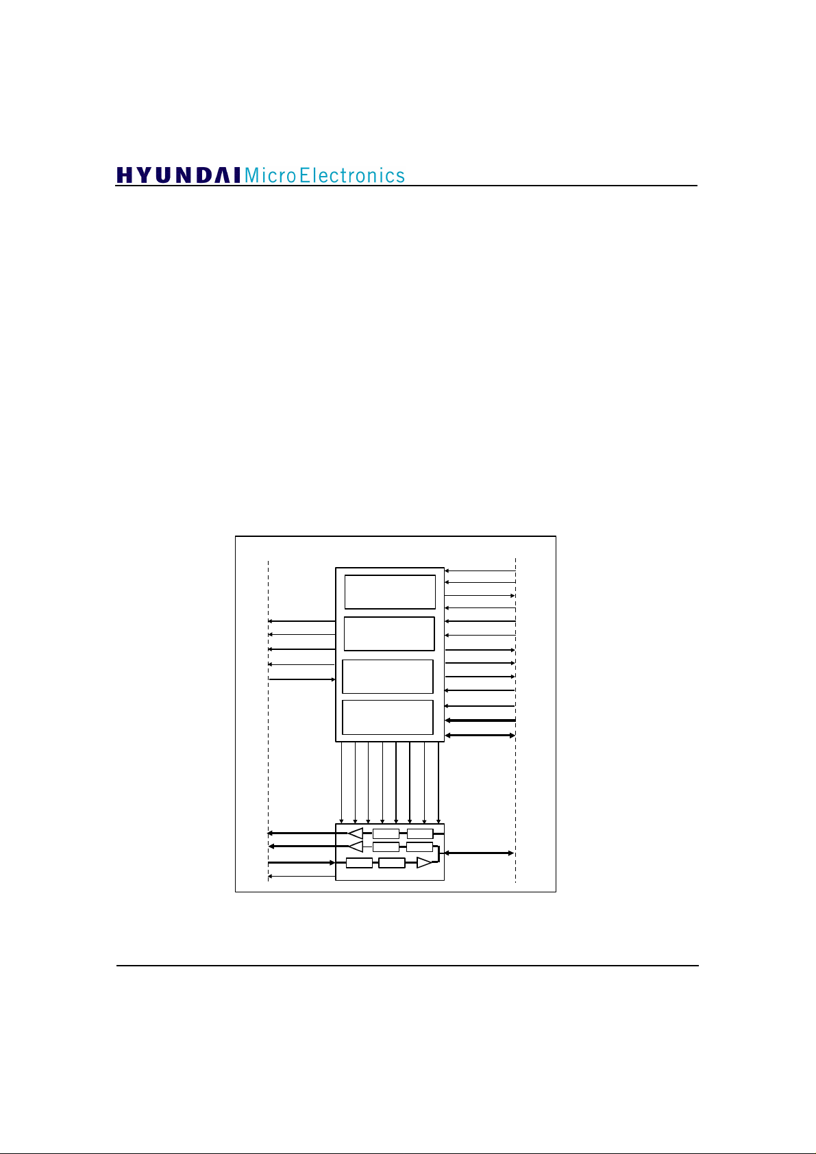
Virtual Address Bus
MMU
Data and
Address
Buffers
AMBA Interface
AMBA Bus
Interface
8KB Cache
Internal Data Bus
Control and
Clocking
Logic
ARM7TDMI
CPU
System
Control
Coprocessor
Figure 1. ARM720T Block Diagram
JTAG
Debug
Interface
Coprocessor
Interface
25
3. Core Block Diagram
A [31:0]
ALE ABE
Address Register
P
C
b
u
Incrementer
s
A
L
U
b
u
s
Register Bank
(31 x 32-bit registers)
(6 status registers)
A
Multiplier
b
u
s
Barrel Shifter
32-bit ALU
Write Data Register
nENOUT nENINDBE
32 x 8
m
Address
B
Instruction Pipeline
& Read Data Register
& Thumb Instruction Decoder
I
n
c
r
e
e
n
t
e
r
b
u
s
b
u
s
D [31:0]
Scan
Control
Instruction
Decoder
&
Control
Logic
DBGRQI
BREAKPTI
DBGACK
ECLK
nEXEC
ISYNC
BL [3:0]
APE
MCLK
nWAIT
nIRQ
nFIQ
nRESET
ABORT
SEQ
LOCK
nCPI
CPA
CPB
nM [4:0]
TBE
TBIT
HIGHZ
Core
ScanChain2
ICE
Breaker
Bus
Splitter
GDC21D601
RANGEOUT0
RANGEOUT1
ESTERN1
EXTERN0
nRW
MAS [1:0]
nTRANS
nMREQ
nOPC
A [0:31]
D [0:31]
DIN [0:31]
DOUT [0:31]
Scan
Chain 0
Scan
Chain 1
TAP Controller
TASPM [3:0]IR [3:0]SCREG [3:0]
Figure 2. ARM7TDMI Core Block Diagram
TCKTMSnTRSTTDITDO
26
GDC21D601
Section 4. DRAM Controller
1. General Description
The DRAM controller interfaces the AMBA Advanced System Bus (ASB) to external DRAM memory banks. The
DRAM controller provides the following features:
• Up to two banks of DRAM support.
• Fast page-mode sequential access support.
• EDO DRAM support
• Word, Half-word and Byte transaction support.
• Little / Big Endian Format support.
• DRAM refresh controller using CAS-before-RAS (CBR) refresh mode.
• Programmable refresh rate.
• Power-down mode where all DRAM accesses (including self-refresh) are disabled.
• Programmable DRAM timing control.
• Row/column addresses multiplexes according to DRAM capacity.
Chip PAD
nDRAMWE
nDRAMOE
nRAS[1:0]
nCAS[3:0]
nCASFB[3:0]
Aout[23:0]
DataOut[31:0]
DataIn[31:0]
nOutEn[3:0]
DRAM Controller
Main State Machine
Address Generator
EBI Signal Control
nDRAMALatch
&
Control
Refresh
Timer & Controller
ASB Interface
&
nDRAMAMUX
nDRAMA[12:0]
nDRAMOutLEn
nDRAMInLEn[3:0]
nDRAMOutEn[3:0]
Lat
Lat
mux
Lat
nDRAMInEn
DRAMByte[1:0]
mux
mux
ASB Bus
BCLK
PDREQ
PDACK
DSELDRAM
DSELREG
BnRES
BLAST
BERROR
BWAIT
BWRITE
BSIZE[1:0]
BA[29:0]
BD[31:0]
BD[31:0]
Figure 1. DRAM Controller Module Block Diagram
27
GDC21D601
2. Hardware Interface and Signal Description
The DRAM Controller module is connected to the ASB bus. Table 1. DRAM interface ASB signal descriptions
shows the internal bus interface signals to the DRAM controller.
Table 1. DRAM Interface ASB Signal Descriptions
NAME DESCRIPTION
BA [27:0] System address bus (excluding high order bits).
BCLK The ASB clock timing all bus transfers.
BD [7:0] Bidirectional system data bus.
BERROR Error slave response signal. It is driven to phase 1 if the DRAM controller is selected. This
signal will be asserted, when an access to the DRAM is attempted while the DRAM
controller is in its Power Down mode.
BLAST Last transfer of burst slave response signal. It can be driven to phase 1 if the DRAM
controller is selected. It is asserted in order to indicate a 256-word boundary to force a non-
sequential access.
BnRES These signals indicate the reset status of the ASB.
BSIZE [1:0] These signals indicate the size of the transfer that may be byte, half-word, or word.
BWAIT Wait slave response signal. It is driven to phase 1 when the DRAM controller is selected. It
is asserted while the DRAM transaction is uncompleted.
BWRITE When this signal is HIGH, it indicates a write transfer and when LOW a read.
DSELDRAM When this signal is HIGH, it indicates that the DRAM is selected.
DSELREG When this signal is HIGH, it indicates that the DRAM configuration register is selected.
Table 2. DRAM interface External DRAM signal descriptions describes the DRAM controller connections to
external devices of the system and to EBI (External Bus Interface) block .
Table 2. External DRAM Signal Descriptions
NAME DESCRIPTION
nRAS[1:0] Active LOW Row Address Strobes, one for each DRAM bank.
NCAS[3:0] Active LOW Column Address Strobes, one for each byte.
NDRAMOE Active LOW Output Enable.
NDRAMWE Active LOW Write Enable.
nCASFB[3:0] This is the nCAS[3:0] signal fed back from the output of the nCAS[3:0] pads.
PDREQ Power Down Request. This signal indicates that the DRAM controller should enter into its
low-power state, causing the DRAMs to enter into self-refresh state if refresh is enabled.
When it is deasserted, the DRAM controller will exit from low power state.
PDACK Power Down Acknowledge. This signal is asserted when the DRAM controller has
successfully entered into its low-power mode. At this point BCLK may be stopped safely. It
is deasserted when the DRAM controller has successfully exited from its low power state.
DRAMAMUX DRAM Address Multiplex Select. When this signal is HIGH, it indicates to the EBI that the
DRAMA[12:0] address should be used to generate DRAMA[12:0]. This signal provides the
support for a shared EBI, and may not be needed in a system where the DRAM controller
does not share the EBI with other memory controllers. DRAMAMUX is LOW when
DRAM accesses are not performed.
28
GDC21D601
NAME DESCRIPTION
NDRAMALatch DRAM Address Latch. When this signal is LOW, it opens the EBI address latch. This
signal is HIGH when DRAM operations do not occur. This signal provides support for a
shared EBI and may not be needed in a system where the DRAM controller does not share
the EBI with other memory controllers.
DRAMA[12:0] These multiplexed address lines are connected to the DRAM Address.
NDRAMInEn DRAM Input Enable. When this signal is LOW, it enables the EBI drivers from latched XD
to BD. This signal is HIGH when DRAM read operations are not performed.
NDRAMInLEn[3:0] DRAM Input Latch Enable. When this signal is HIGH, it shuts the EBI latches on XD. This
signal is LOW when DRAM read operations are not performed.
NDRAMOutEn DRAM Output Enable. When this signal is HIGH, it disables the EBI drivers from latched
BD to XD. This signal is low when DRAM write operations are not performed.
NDRAMOutLen DRAM Output Latch Enable. When this signal is LOW, it opens the EBI latches on BD.
This signal is HIGH when DRAM write operations are not performed.
Accesses to the DRAM Controller module are generated as a result of the address decode put out on the ASB
address bus by the current bus master (which could be the ARM CPU or the DMA engine, for example).
The following three diagrams show the timing of the external interface for read, write and refresh cycles
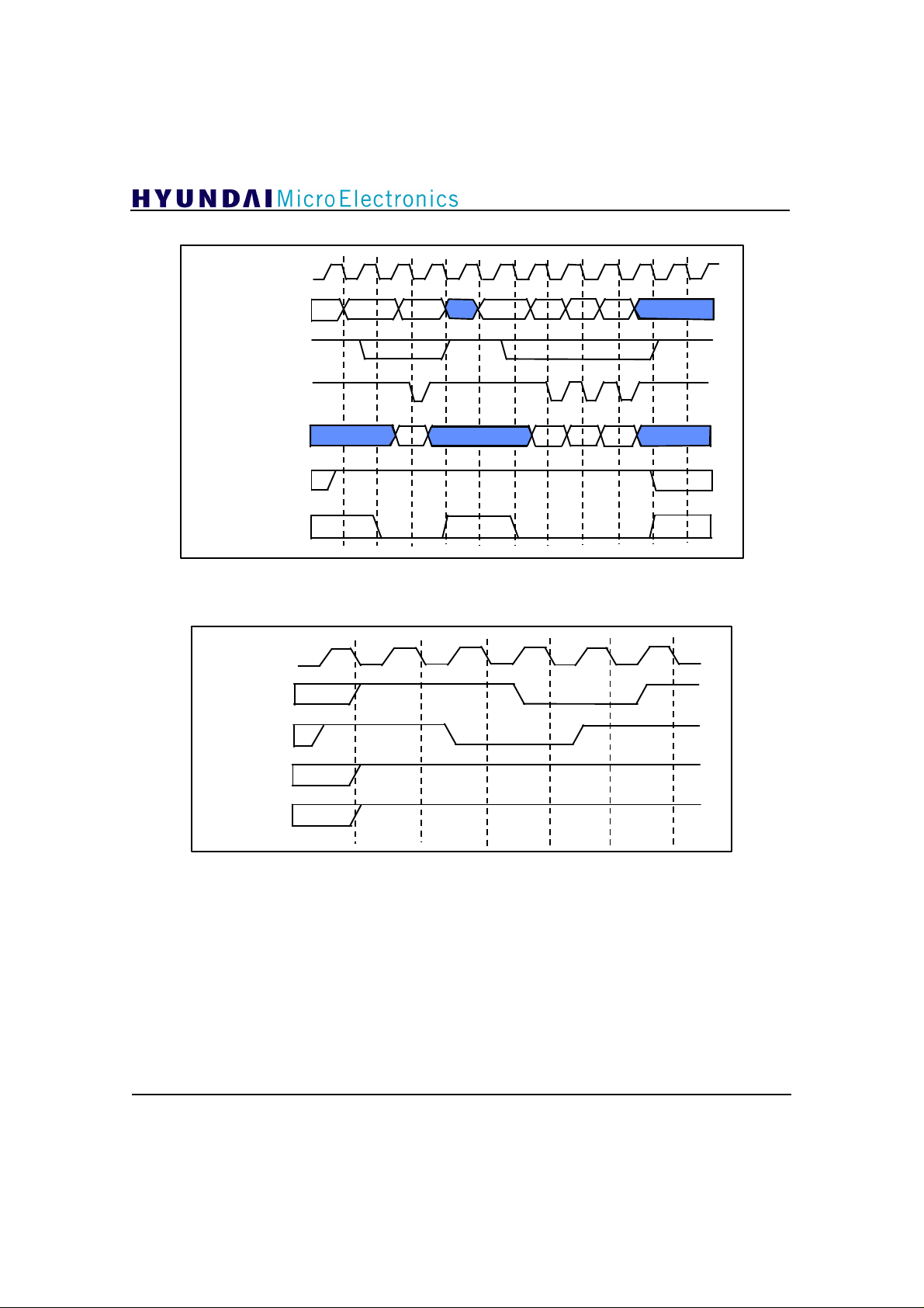
(Figure 2, 3, 4).
BCLK
DRAMA[12:0]
nRAS[1:0]
nCAS[1:0]
XData[31:0]
nOE
nWE
row
Figure 2. DRAM External Signal Timing: Read Cycles
col row col1 col2
col3
29
BCLK
GDC21D601
DRAMA[12:0]
nRAS[1:0]
nCAS[1:0]
XData[31:0]
nOE
nWE
BCLK
nRAS[1:0]
nCAS[1:0]
row
col row col1 col2
Data
Data1
col3
Data2 Data3
Figure 3. DRAM External Signal Timing: Write Cycles
30
nOE
nWE
Figure 4. DRAM Controller Refresh Cycle
GDC21D601
3. Functional Description
3.1 Introduction
The DRAM controller provides connections allowing a direct interface to up to two banks of DRAM. Each bank is
32/16/8 bits wide and up to 256MB in size. Two RAS lines are provided (one per bank) and four CAS lines (one
per byte line).
3.2 Functional BreakDown
The DRAM controller consists of four main blocks: the Main State Machine & Control Block, the EBI Signal
Control Block, the ASB Interface & Address Generation Block, and the Refresh Timer & Counter Block.
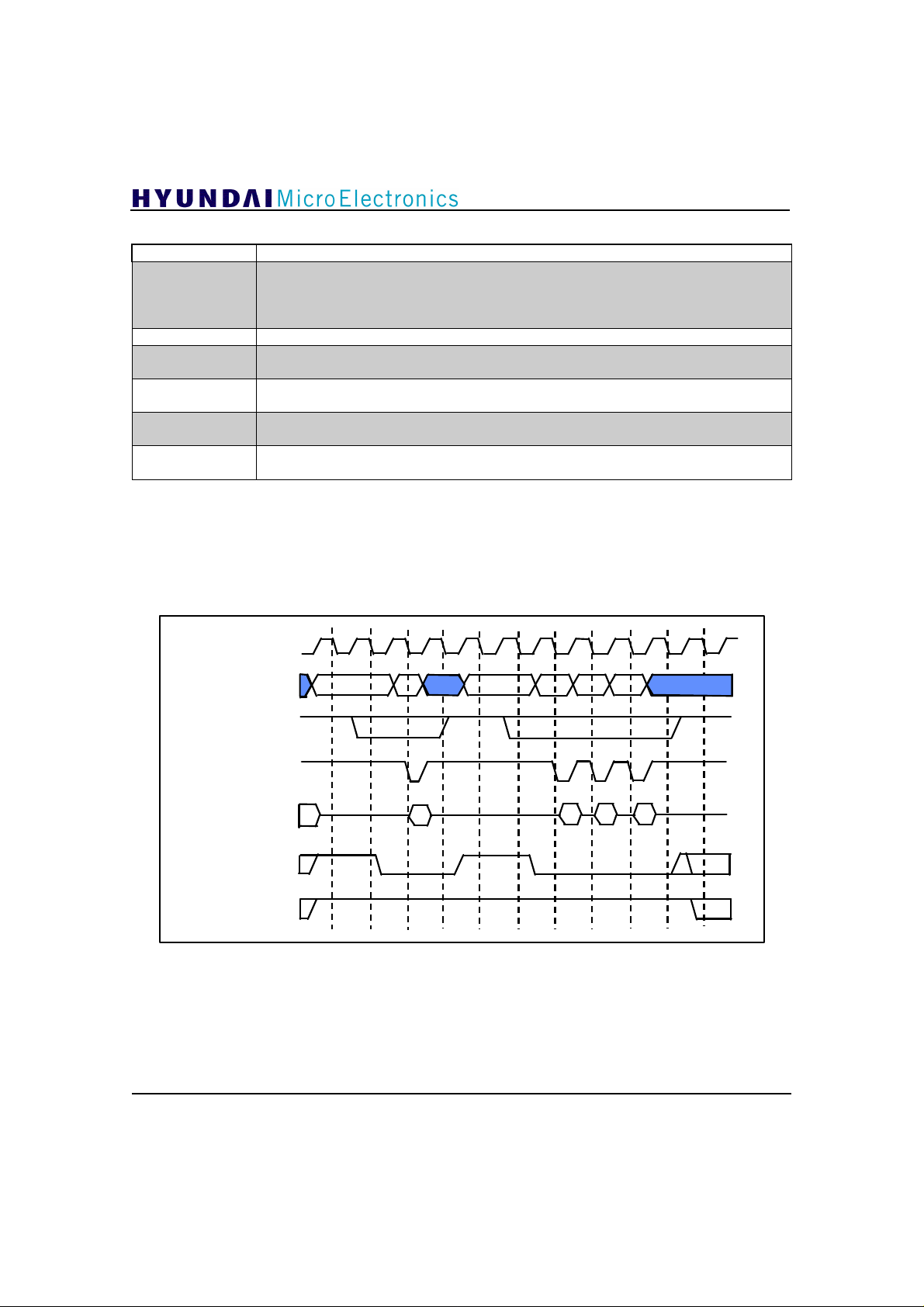
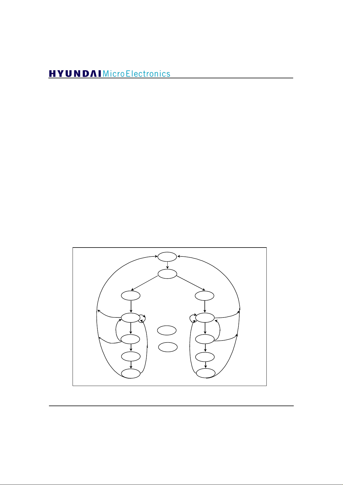
3.3 Main State Machine
This block contains the main DRAM timing control state machine and the decode for the external strobe signals
for the DRAM interface. The state machine generates the timing for the nCAS and nRAS strobes, and the
multiplexing of the DRAM row and column address lines for standard DRAM cycles and refresh cycles. The
nDRAMWE and nDRAMOE signals are asserted appropriately depending on the access type. Word, Half-word,
and Byte accesses are decoded from the lower bits of the BA address bus in order to assert the appropriate nCAS
line(s). For word accesses all four nCAS lines are asserted. Figure 5. Descibes the Main State Machine Diagram.
Local arbitration for refresh cycles is also carried out here as refresh requests are received from the refresh timer
block. The block also supports the self refresh DRAM; enter to and exit from this self refresh state are initiated by
the PDRREQ signal. This is illustrated in Figure 6. DRAM signal timing: power down mode.
RefReq or
!DSEL
r_IDLE
DSEL
r_RnR
CAS
r_RnC1
CAS
r_RnC2
r_RnC3
r_RnC4
!BWRITE
r_WAIT
RAS
r_CRWAIT
r_CWWAIT
BWRITE
r_WnR
r_WnC1
r_WnC2
r_WnC3
r_WnC4
Figure 5. Main State Machine Diagram
CAS
CAS
RefReq or
!DSELD1
31
 Loading...