

HEI GDC21D401B Datasheet

GDC21D401B
(Video Decoder)
Version 1.0
Mar, 99
HDS-GDC21D401B-9908 / 10

GDC21D401B
The information contained herein is subject to change without notice.
The information contained herein is presented only as a guide for the applications of our products. No
responsibility is assumed by Hyundai for any infringements of patents or other rights of the third
parties which may result from its use. No license is granted by implication or otherwise under any
patent or patent rights of Hyundai or others.
These Hyundai products are intended for usage in general electronic equipment (office equipment,
communication equipment, measuring equipment, domestic electrification, etc.).
Please make sure that you consult with us before you use these Hyundai products in equipment which
require high quality and / or reliability, and in equipment which could have major impact to the welfare
of human life (atomic energy control, airplane, spaceship, traffic signal, combustion control, all types
of safety devices, etc.). Hyundai cannot accept liability to any damage which may occur in case these
Hyundai products were used in the mentioned equipment without prior consultation with Hyundai.
Copyright 1999 Hyundai Micro Electronics Co.,Ltd.
All Rights Reserved
3

GDC21D401B
TABLE OF CONTENTS
1. General Description............................................................................................................5
2. Features...............................................................................................................................5
3. Pin Description....................................................................................................................6
4. Block Diagram...................................................................................................................10
5. Functional Description ..................................................................................................... 11
5.1 Initialization and Decoding Start...................................................................................11
5.2 Picture Decoding..........................................................................................................11
5.3 STC (System Time Clock) Generation..........................................................................12
5.4 DTS (Decoding Time Stamp) Synchronization..............................................................12
5.5 Error Concealment.......................................................................................................12
5.6 User Data Read............................................................................................................ 12
5.7 Bitstream Buffer Over/Underflow ..................................................................................13
5.8 VLD (Variable Length Decoder)....................................................................................13
5.9 Inverse Quantization ....................................................................................................13
5.10 IDCT (Inverse Discrete Cosine Transform).................................................................13
5.11 MC(Motion Compensation).........................................................................................13
5.12 Transport Interface.....................................................................................................14
5.13 Host Interface.............................................................................................................15
5.14 Video Data Output Format.......................................................................................... 20
5.15 Video Data Output Timing..........................................................................................21
5.16 SDRAM Interface .......................................................................................................22
6. Electrical Specification..................................................................................................... 24
6.1 Absolute Maximum Rating............................................................................................24
6.2 Recommended Operating Range .................................................................................24
6.3 DC Characteristics (VDD = 3.3 V±10%, TA = 0 ~ 70¡É)................................................24
6.4 AC Characteristics (VDD = 3.3 V±10%, TA = 0 ~ 70¡É) ................................................25
7. Package Mechanical Data.................................................................................................26
7.1 Package Pin Out .......................................................................................................... 26
7.2 Physical Dimension...................................................................................................... 29
4

GDC21D401B
GDC21D401B
Video Decoder
1. General Description
The Video Decoder(VD) decodes video
elementary stream of MPEG-2(ISO/ICE
13818-2)MP@HL. It supports the ATSC
digital TV video standard, and can be used for
the video part of the ATSC digital TV with the
Transport Decoder and the VDP(Video
Display Processor). Picture decoding timing
can be controlled internally for A/V lip
synchronization, and externally for Video
Trick Mode by host microprocessor via I2C bus.
The Video Decoder can extract video user data
including caption from video elementary
stream, and host microprocessor can read the
video user data from the Video Decoder(VD)
via I2C. It uses four 16x1M SDRAMs and can
support up to 81 MHz memory clock speed.
2. Features
• Supports MPEG-2 (ISO/ICE 13818-2)
MP@HL
• Supports all video input formats of ATSC
digital TV standard
• Supports picture decoding capability up to
1920x1088 30 Frame/Sec
• Supports all kinds of motion compensation
methods of MPEG-2
• Supports MPEG-2 error code, syntax error
detection, and slice-based error concealment
• Supports DTS synchronization
• Supports VBV delay mode and low delay
mode decoding
• Supports film mode decoding (3:2 Pull
down)
• Supports high level commands for trick
mode
• Supports 8(w)x64(d) internal user data FIFO
• Outputs: macroblock format
4-pel parallel output
54 MHz synchronous I/F
Data window (pdwin, sclk, and mbclk)
Picture information (Picture structure, Field
parity, and DCT type)
• External memory for VBV buffer , DTS
FIFO and 2-frame memory:
64-bit Data Bus
81 MHz Synchronous Interface
64-Mbyte
Four 16x1M SDRAMs
• Host processor interface: I2C bus interface
Two interrupt signals
Supports 23 programmable internal
registers
5
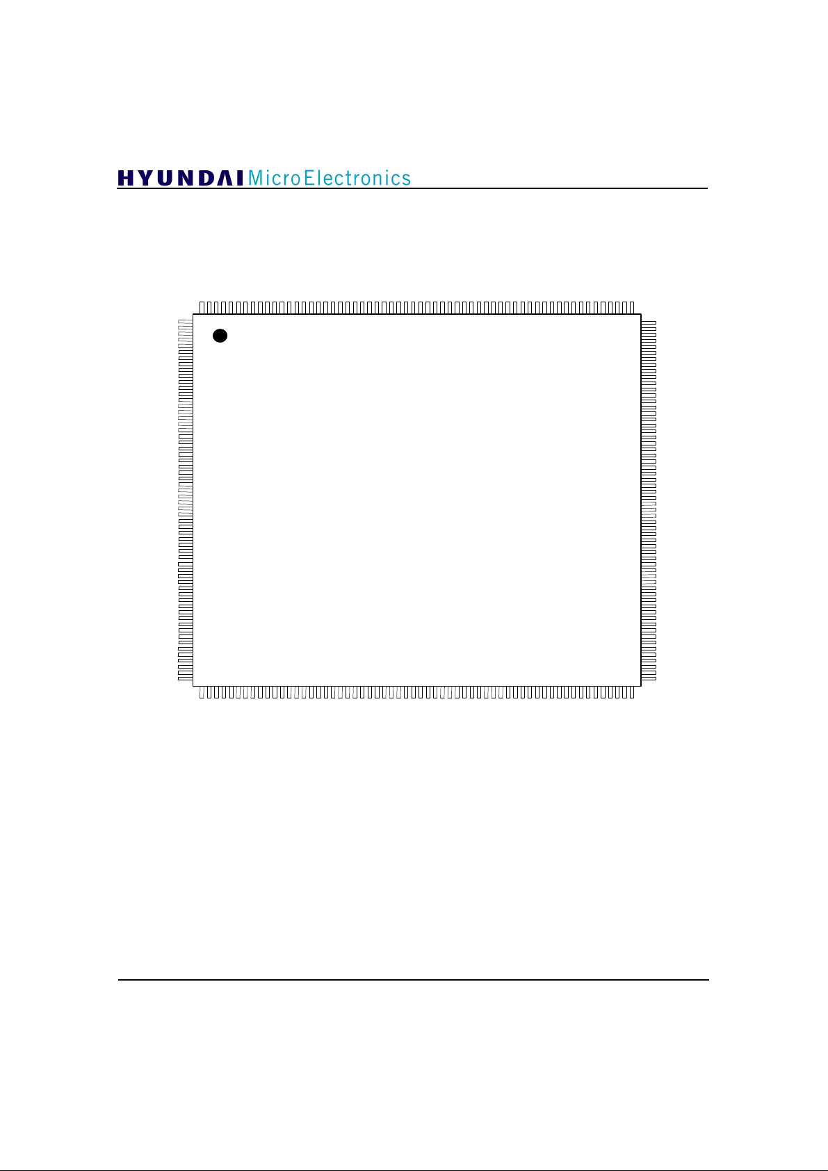
3. Pin Description
60
HME
SDRAM_DATA[38]
VDD
SDRAM_DATA[37]
SDRAM_DATA[36]
P_SHARE_
P_SHARE_
P_SHARE_
MCLK_OUT
TEST_ OUT[2]
FP_FD
MCLK_IN
DEC_ERROR
VSS
P_WAIT
PIC_DIS_SYNC
VDD
VDD
PDATA[31]
PDATA[30]
PDATA[29]
PDATA[28]
VSS
VSS
PDATA[27]
PDATA[26]
PDATA[25]
PDATA[24]
VDD
PDATA[23]
PDATA[22]
PDATA[21]
PDATA[20]
VSS
PDATA[19]
PDATA[18]
VDD
PDATA[17]
PDATA[16]
PDATA[15]
VDD
PDATA[14]
PDATA[13]
PDATA[12]
VSS
PDATA[11]
VSS
PDATA[10]
VDD
PDATA[9]
PDATA[8]
VDD
PDATA[7]
PDATA[6]
PDATA[5]
PDATA[4]
VSS
VSS
PDATA[3]
VDD
VDD
PDATA[2]
PDATA[1]
PDATA[0]
VSS
5101520253035
40
45
50
55
65
7075808590
95
100
105
110
115
120
190
185
195
200
205
210
215
220
225
230
235
IN[10]
IN[9]
IN[8]
240
VSS
VDD
VSS
\RESET
TSW
\VIDEN
VSTCW
VSS
VDD
VSS
VDD
VSS
SCL
VSS
SDA
\INT_V
VDD
VSS
VDD
VDD
VDD
VSS
VDD
VSS
VDD
VSS
1
VSS
SDRAM_DATA[20]
VDD
SDRAM_DATA[19]
VSS
SCANTESTON
IDCTTESTON
MEMTESTON
CLK_27M
VID_STRB
VID_DATA[0]
VID_DATA[1]
VID_DATA[2]
VID_DATA[3]
VID_DATA[4]
VID_DATA[5]
VID_DATA[6]
VID_DATA[7]
\VID_REQ
\UBUFF_FULL
SDRAM_DATA[0]
SDRAM_DATA[1]
SDRAM_DATA[2]
SDRAM_DATA[3]
SDRAM_DATA[4]
SDRAM_DATA[5]
SDRAM_DATA[6]
SDRAM_DATA[7]
SDRAM_DATA[8]
SDRAM_DATA[9]
SDRAM_DATA[10]
SDRAM_DATA[11]
SDRAM_DATA[12]
SDRAM_DATA[13]
SDRAM_DATA[14]
SDRAM_DATA[15]
SDRAM_DATA[16]
SDRAM_DATA[17]
SDRAM_DATA[18]
VDD
SDRAM_DATA[21]
VSS
SDRAM_DATA[22]
VDD
SDRAM_DATA[23]
SDRAM_DATA[25]
SDRAM_DATA[24]
GDC21D401B
YYWWA
VSS
MCLK
VDD
SDRAM_ADDR[6]
SDRAM_ADDR[1]
VDD
SDRAM_ADDR[5]
VDD
SDRAM_ADDR[2]
SDRAM_ADDR[4]
VSS
SDRAM_ADDR[3]
VSS
SDRAM_DATA[31]
SDRAM_DATA[30]
VDD
SDRAM_DATA[29]
SDRAM_DATA[28]
VSS
SDRAM_DATA[27]
SDRAM_DATA[26]
VDD
GDC21D401B
VSS
180
PSTR[1]
PSTR[0]
PDWIN
VSS
175
D_INFO_WIN
DIS_INFO
VDD
VDD
\FFPN
170
VSS
MBFI
MBCLK
VDD
SCLK
165
VDCLK
VSS
SDRAM_DATA[63]
SDRAM_DATA[62]
SDRAM_DATA[61]
160
VDD
VDD
SDRAM_DATA[60]
SDRAM_DATA[59]
VSS
155
VSS
SDRAM_DATA[58]
VDD
SDRAM_DATA[57]
VSS
150
SDRAM_DATA[56]
VDD
SDRAM_DATA[55]
SDRAM_DATA[54]
VSS
145
SDRAM_DATA[53]
SDRAM_DATA[52]
VDD
SDRAM_DATA[51]
SDRAM_DATA[50]
140
VSS
SDRAM_DATA[49]
SDRAM_DATA[48]
VDD
SDRAM_DATA[47]
135
VDD
SDRAM_DATA[46]
SDRAM_DATA[45]
VSS
VSS
130
SDRAM_DATA[44]
VDD
SDRAM_DATA[43]
VDD
SDRAM_DATA[42]
125
SDRAM_DATA[41]
VSS
SDRAM_DATA[40]
VSS
SDRAM_DATA[39]
SDRAM_DATA[35]
VSS
SDRAM_DATA[34]
SDRAM_DATA[33]
SDRAM_DATA[32]
VDD
VDD
CSN
RASN
CASN
WEN
VSS
BA0
SDRAM_ADDR[10]
SDRAM_ADDR[9]
SDRAM_ADDR[8]
VDD
SDRAM_ADDR[7]
SDRAM_ADDR[0]
VSS
VSS
6
Figure 1. Pin Description
(Package: 240 HQFP)
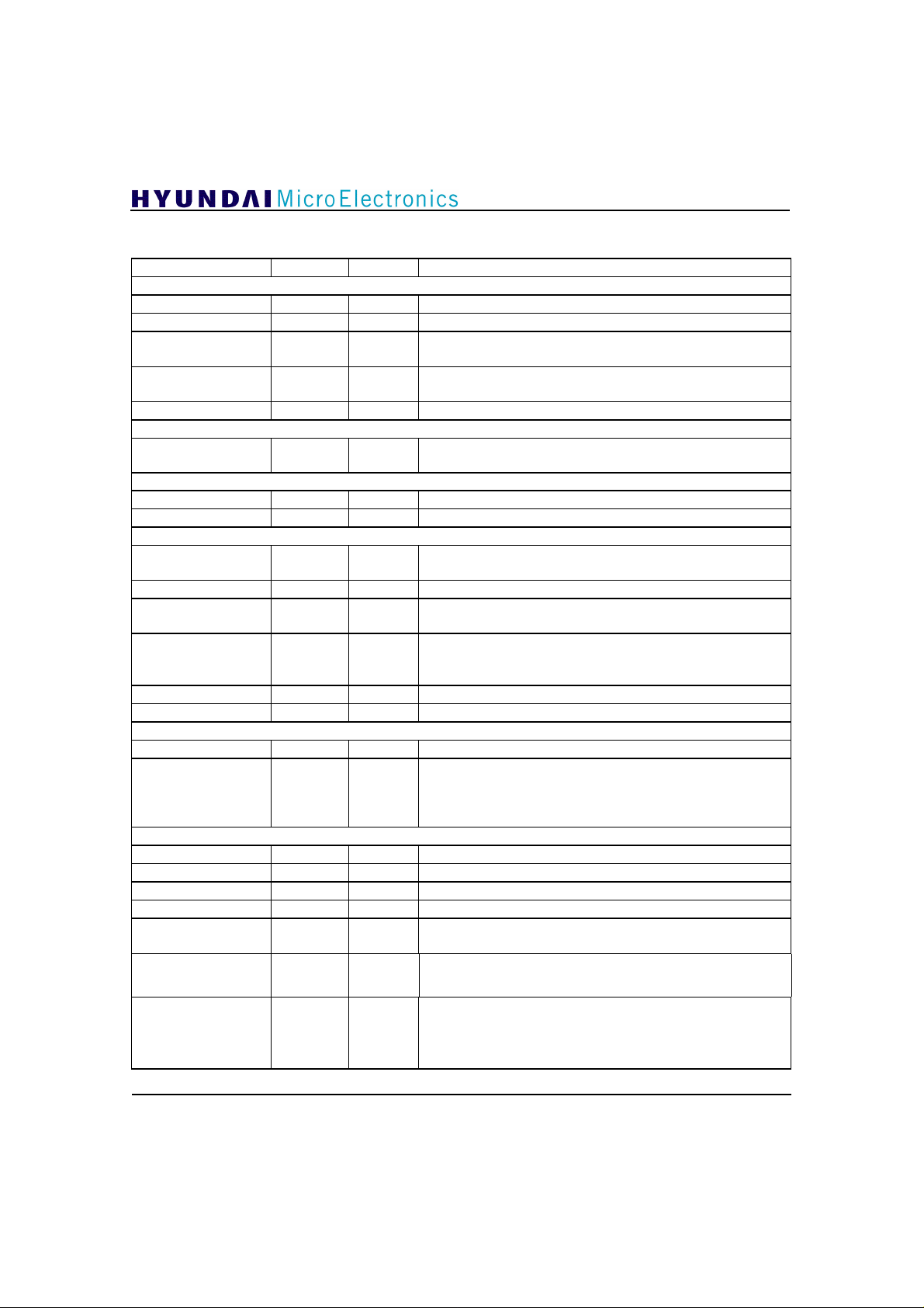
NAME PIN TYPE DESCRIPTION
VDCLK
MCLK
MCLK_IN
MCLK_OUT
CLK_27M
\RESET
SCL
SDA
VID_DATA[7:0]
\VID_REQ
VID_STRB
TSW
\VIDEN
VSTCW
\INT_V
\UBUFF_FULL
CSN
WEN
RASN
CASN
BA0
SDRAM_ADDR
[10:0]
SDRAM_DATA
[63:0]
25,23,21,20,
CLOCK
165 I
94 I
234
237
6 I
O
Operating clock. - 54 MHz (max), 50 % duty cycle
SDRAM interface clock. - 81 MHz (max), 50 % duty cycle
SDRAM interface clock. - 81 MHz (max),
I
50 % duty cycle (the same clock as MCLK)
SDRAM interface clock through clock buffer for delay effect.
This signal input is MCLK_IN.
External system time clock. - 27 MHz
RESET
8 I Power on reset(active low). At least 3 VDCLKs.
Decoding starts after 128 VDCLKs from the last reset low state.
I2C-BUS INTERFACE
26 I
28 I/O
I2C-bus serial clock. - 400 KHz(max)
I2C-bus serial data
TRANSPORT INTERFACE
I
Transport Decoder data bus
18,16,15,14
29 O
13 I
Transport data request(active low)
Transport data strobe.
VID_DATA[7:0] is latched on the rising edge.
9 I
PTS & DTS data enable(active high).
In LG DTV chipset, this signal is connected to the
PTS_DTS_STRB pin of GDC21D301A.
10 I
11 I
Video bitstream data enable(active low)
STC data enable(active high)
HOST INTERRUPT
31 O
30 O
Video decoder interrupt(active low)
User data FIFO is full(active low).
When it happens, host microprocessor must read the user data
from user data FIFO.
Otherwise video decoder suspends decoding.
SDRAM INTERFACE
109 O
106 O
108 O
107 O
104 O
SDRAM chip selection(active low)
SDRAM write enable(active low)
SDRAM row address selection(active low)
SDRAM column address selection(active low)
SDRAM bank address.
This indicates bank address, and low value selects bank ‘0’ .
103,102,101,
99,92,89,86,
84,87,91,98
163,162,161,
158,157,154,
152,150,43,
42,40,39,38,
36, 34, 33
O
I/O
SDRAM address
SDRAM data bus
GDC21D401B
7
Pin Description (continued)
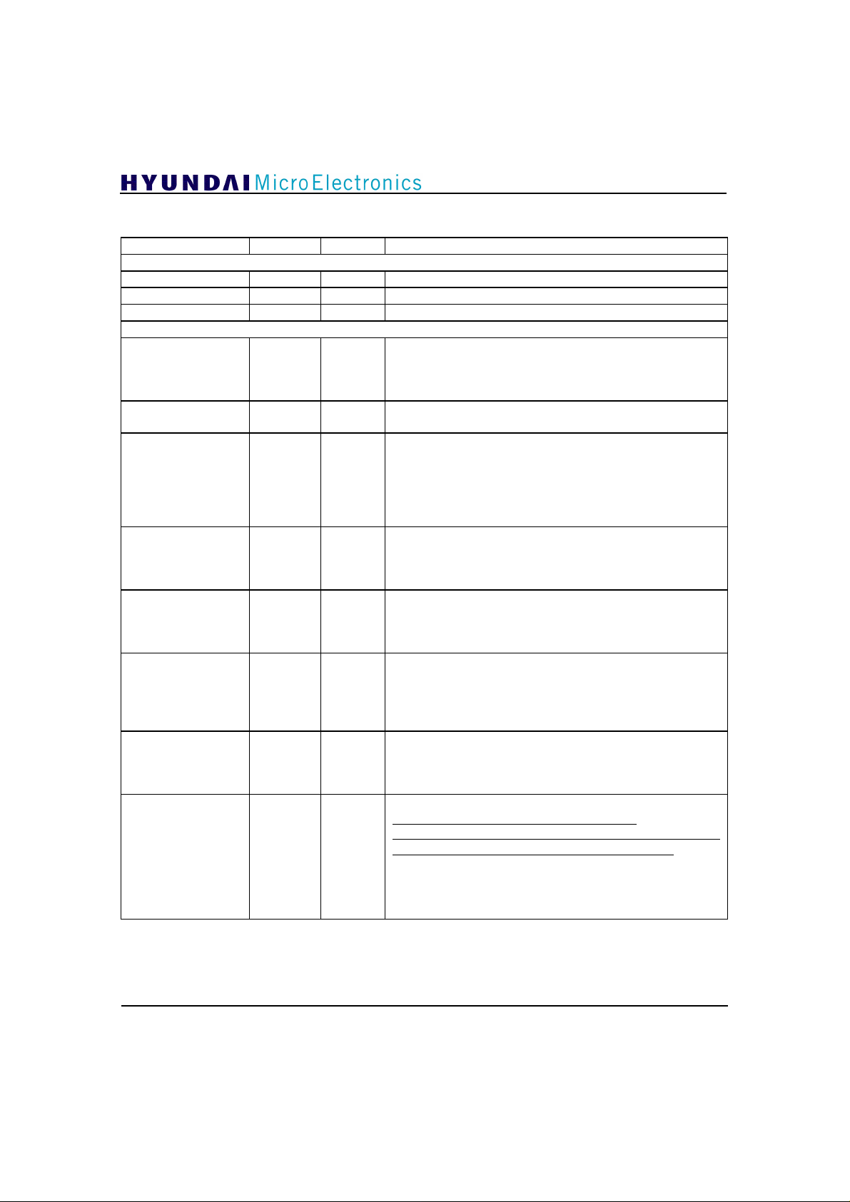
NAME PIN TYPE DESCRIPTION
VDP INTERFACE - SYNC & PICTURE FORMAT
DIS_INFO
D_INFO_WIN
PIC_DIS_SYNC
P_WAIT
PDWIN
PSTR[1:0]
\FFPN
SCLK
MBCLK
DEC_ERROR
FP_FD
174 O
175 O
230 I
231 I
177 O
179,178 O
171 O
166 O
168 O
233 O
235 O
GDC21D401B
Serialized picture format data
Serialized picture format data enable(active high)
Picture display sync. - 30 Hz or 29.97 Hz, 50% duty
VDP INTERFACE – PICTURE DATA
PDATA wait(active high).
This signal makes PDATA output to be suspended after 50
VDCLKs from the last high value.
This signal is the output of the VDP.
Picture data window(active high).
During 1 picture data decoding, this signal is high.
Picture structure.
This indicates the structure of output picture.
If this is equal to ‘1’ , the output picture is top field picture.
If this is equal to ‘2’ , the output picture is bottom field
picture.
If this is equal to ‘3’ , the output picture is frame picture.
First field parity(active low).
This signal is the first_field_parity flag of output picture.
When output picture is interlaced frame picture, the field of
output frame is the first output by the VDP.
Slice decoding window(active high).
This signal has high value when a macroblock with the same
vertical position is decoded. There are at least 2-clock low
value periods between each slice decoding window.
Macroblock decoding window(active high).
This signal has high value when a macroblock data is
decoded. The width of high value is always 96 VDCLKs.
There are at least 2-clock low value periods between each
macroblock decoding window.
Decoding Error (active high)
This is a multiplexed output signal.
It is used to inform VDP R1.2 (GDC21D701B) of an error in
Picture or Macro Block.
Frame_Pred_Frame_Dct (active high)
This signal is explained in ISO/IEC 13818-2
(Information technology – Generic coding of moving
pictures and associated audio information : Video)
If this flag is set to ‘1’ , only frame_DCT and frame prediction
are used. In a field picture, it should be ‘0’ .
If progressive_frame is ‘1’ , Frame_pred_frame_dct should be
set to ‘1’ . This flag affects the syntax of the bitstream.
8
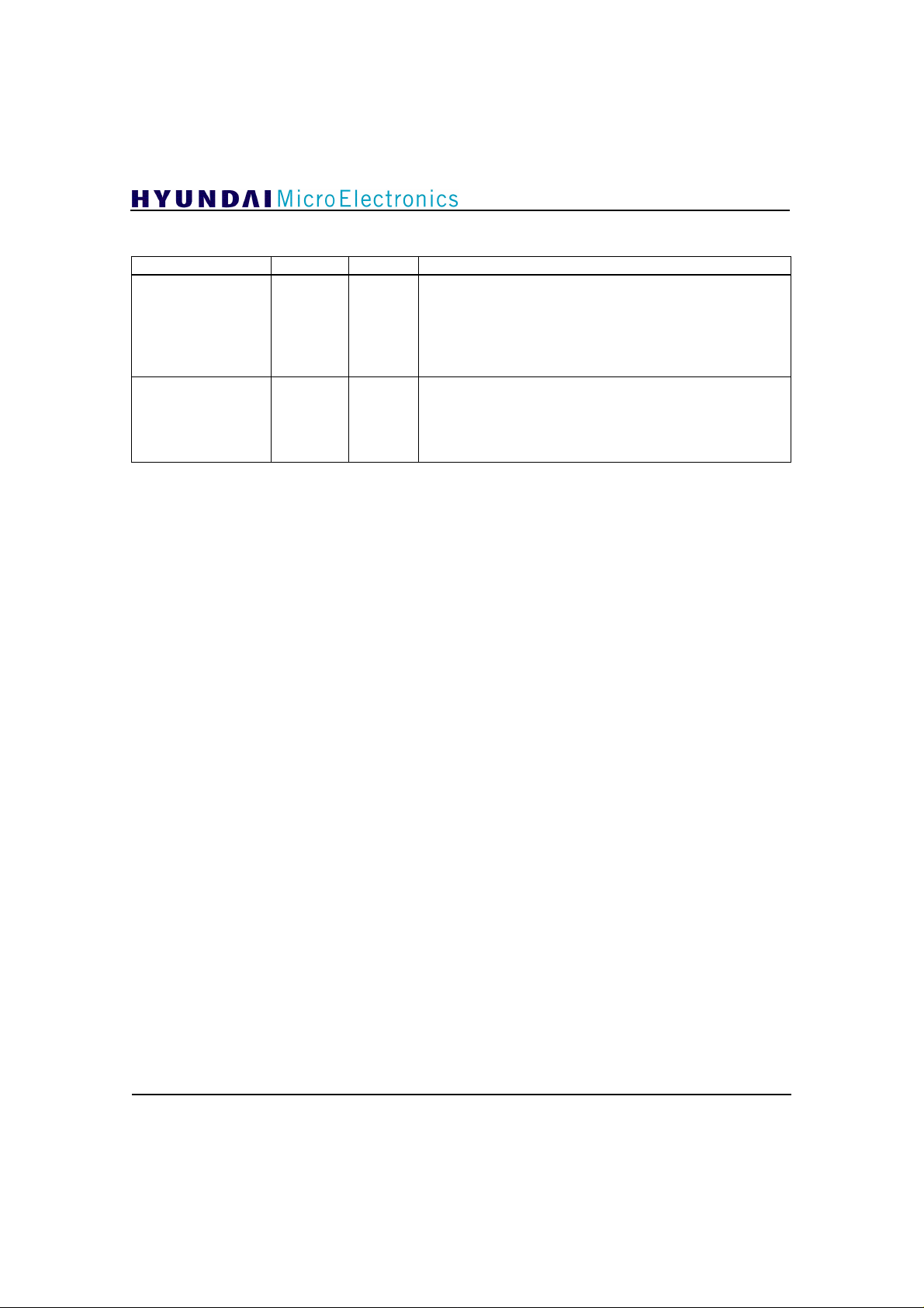
Pin Description (continued)
227,226,225,
224,221,220,
191,190,187,
NAME PIN TYPE DESCRIPTION
MBFI
PDATA[31:0]
169 O
184,183,182
GDC21D401B
Macroblock Field IDCT.
This signal has the meaning when a decoded picture is a frame
picture. If this is set to ‘0’ , the output of a decoded
macroblock has the form of frame IDCT.
If this is set to ‘1’ , the output of a decoded macroblock has the
form of field IDCT.
O
Picture data.
This is a bundle of four adjacent pixel data.
A decoded macroblock consists of 96 consequent PDATA.
The order of PDATA in a decoded macroblock depends on the
MBFI signal.
9
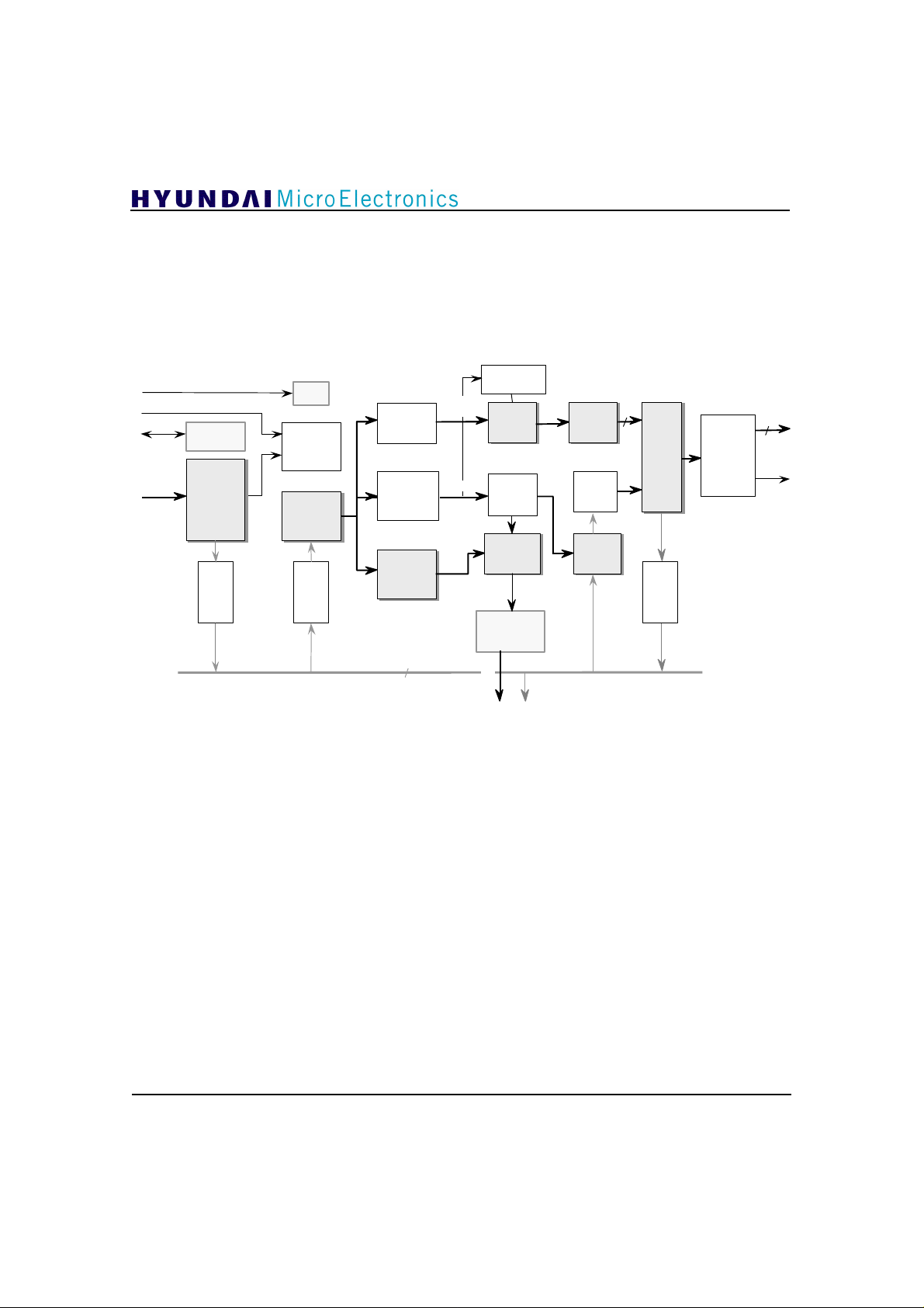
4. Block Diagram
GDC21D401B
MHz System Clock
27
Display Sync
Video
Bitstream
I C I/F
2
Video
Bitstream
Predecoder
FIFO
STC
DTS check
Decoding
Controller
Sequence
Parcer
FIFO
IDCT
Coefficient
Decoder
Macroblock
Parameter
Decoder
Motion
Vector
Decoder
64
Internal Data Bus
IDCT
coefficients
MB
parameters
MB
Motion
Vector
Quantization
Matrix
IQ
IQ
&
&
Buffer
Buffer
MB
Decoding
Controller
MV
Processor
SDRAM
Controller
Address
Data
Max. M sample/sec
200
High-Speed IDCT
32
IDCT
IDCT
FIFO
Half-pel
Predictor
Predictor
FIFO
Display
Processor
Control
Decoded
MB Data
32
Data
Window
10
Figure 2. MPEG-2 MP@HL Video Decoder Block Diagram
 Loading...