

HEI GDC21D301A Datasheet

GDC21D301A
(Transport Decoder)
Version 1.5
HDS-GDC21D301A-9908 / 10

GDC21D301A
The information contained herein is subject to change without notice.
The information contained herein is presented only as a guide for the applications of our products. No
responsibility is assumed by Hyundai for any infringements of patents or other rights of the third parties
which may result from its use. No license is granted by implication or otherwise under any patent or
patent rights of Hyundai or others.
These Hyundai products are intended for usage in general electronic equipment (office equipment,
communication equipment, measuring equipment, domestic electrification, etc.).
Please make sure that you consult with us before you use these Hyundai products in equipment which
require high quality and / or reliability, and in equipment which could have major impact to the welfare of
human life (atomic energy control, airplane, spaceship, traffic signal, combustion control, all types of
safety devices, etc.). Hyundai cannot accept liability to any damage which may occur in case these
Hyundai products were used in the mentioned equipment without prior consultation with Hyundai.
Copyright 1999 Hyundai Micro Electronics Co.,Ltd.
All Rights Reserved
3

GDC21D301A
TABLE OF CONTENTS
1. General Description.................................................................................................................5
2. Features....................................................................................................................................5
3. Pin Description.........................................................................................................................6
4. Block Diagram........................................................................................................................12
5. Functional Description..........................................................................................................13
5.1 Forward-Error-Correction (FEC) Interface........................................................................13
5.2 Sync Detector ...................................................................................................................13
5.3 TS Header Decoder..........................................................................................................13
5.4 Adaptation Field Decoder.................................................................................................13
5.5 PES Decoder....................................................................................................................13
5.6 Memory Controller............................................................................................................14
5.7 High-Speed Interface........................................................................................................14
5.8 External Decoder Interface...............................................................................................14
5.9 Host Interface ...................................................................................................................14
5.10 Clock Controller ..............................................................................................................14
6. Register Description..............................................................................................................15
7. Electrical Specification..........................................................................................................30
7.1 Absolute Maximum Rating ................................................................................................30
7.2 Recommended Operating Range.....................................................................................30
7.3 DC Characteristics (VDD = 3.3 V ± 10%, TA = 0 ~ 70 °C )..............................................30
7.4 AC Characteristics (VDD = 3.3 V ± 10%, TA = 0 ~ 70 °C )..............................................31
7.4.1 Transport Stream Interface Requirements..................................................................31
7.4.2 Clock Interface Requirements.....................................................................................31
7.4.3 Reset Signal Requirement..........................................................................................32
7.4.4 Audio/Video/Data Decoder Interface Requirements...................................................32
7.4.5 Host Processor Interface Requirements.....................................................................33
8. Package Mechanical Data.....................................................................................................34
8.1 Package Pin out................................................................................................................34
8.2 Package Dimensions........................................................................................................36
4

GDC21D301A
GDC21D301A
Transport Decoder
1. General Description
The GDC21D301A Transport Decoder
resides in the center of an MPEG-2 decoding
system. It accepts MPEG-2 transport streams,
parses the transport and packetized
elementary stream (PES) layers into the
separate data streams, and provides rate
buffering for the parsed data streams. Then it
passes those data streams to video and audio
decoders. The GDC21D301A also extracts
Program Clock Reference (PCR) in the data
stream and provides the Pulse Width
Modulation (PWM) signals in order to
recover the clock and to synchronize the
playback of video and audio. The
GDC21D301A manages an external DRAM
that is used for data storage and buffering the
various parsed data streams. This DRAM is
shared with the host processor so that the
system’s memory requirements can be
consolidated into a single, low-cost DRAM.
The GDC21D301A stores data packets
destined for the host directly in shared
DRAM for easy access by the host.
2. Features
The GDC21D301A is fully compliant with MPEG2 ISO/IEC 13818-1 specification.
Decoding Features
• Performs MPEG-2 transportation and PES layer
handling
• Supports maximum 80 Mbps transport streams
• Provides a high-speed data output port
• Identifies and extracts up to 32 transport stream
(TS) packet PIDs
PCR & Time Stamp Control Features
• Provides two PWM signals to recover the system
clock
• Provides the instant value of internal STC
counter when a frame begins
• Extracts PTS and DTS of video and audio for
Lip-synchronization
Interface
• Supports byte-parallel/bit-serial TS input
• Supports video/audio PES layer or elementary
stream layer output
• Provides error code insertion capability in video
elementary stream
• Supports an external error input signal for
declaring an erroneous packet
• Supports 8/16-bit host bus interface
5
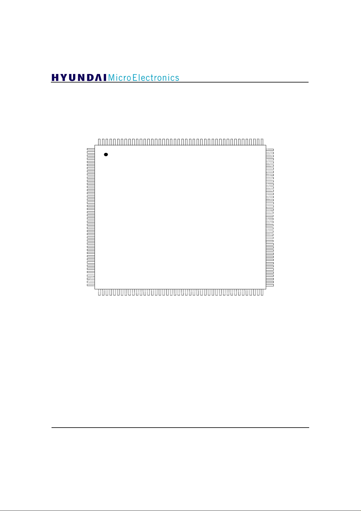
3. Pin Description
45
YYWW
DRAM_DATA[2]
VSS
DRAM_DATA[3]
DATA[4]
DSP_
VDD
DSP_
DSP_
DSP_
DSP_
VSS
DSP_
DSP_
DSP_
DSP_
VDD
DSP_
DSP_
DSP_
DSP_
VSS
NC
VDD
CLOCK
BIT8MODE
DSP_
DSP_
DSP_
DSP_
DSP_
DSP_
DSP_
DSP_
DSP_
DSP_
DSP_
DSP_
DSP_
DSP_
DSP_
DSP_
DSP_
DSP_
DSP_
DSP_
DSP_ADDR[20]
DSP_ADDR[21]
DSP_ADDR[22]
DATA[12]
DATA[11]
DATA[10]
DATA[9]
DATA[8]
DATA[7]
DATA[6]
DATA[5]
DATA[4]
DATA[3]
DATA[2]
DATA[1]
DATA[0]
ADDR[0]
ADDR[1]
ADDR[2]
ADDR[3]
ADDR[4]
ADDR[5]
ADDR[6]
ADDR[7]
ADDR[8]
ADDR[9]
ADDR[10]
ADDR[11]
ADDR[12]
ADDR[13]
ADDR[14]
ADDR[15]
ADDR[16]
ADDR[17]
GDC21D301A
ADDR[18]
ADDR[19]
DSP_DATA[13]
DSP_DATA[14]
DSP_DATA[15]
VSS
DSP_INT
DSP_READY
VDD
TDO0
TDO1
VDD
HSDEN
HIGH_SP_DATA[1]
HIGH_SP_DATA[0]
CLOCK_OUT
VSS
TA[7]
TA[6]
TA[5]
TA[4]
TA[3]
TA[2]
TA[1]
TA[0]
VSS
TWEB
TEST
TDI
P_S_MODE
F_START
FEC_DATA[7]
FEC_DATA[6]
FEC_CLOCK
VDD
VSS
FEC_DATA[5]
FEC_DATA[4]
FEC_DATA[3]
FEC_DATA[2]
FEC_DATA[1]
FEC_DATA[0]
ERR_BLOCK_B
D_VALID
SCAN_MODE/TA[8]
1
133176
HME
GDC21D301A
NC
DRAM_
DRAM_DATA[5]
DRAM_DATA[6]
VDD
DRAM_DATA[7]
DRAM_DATA[8]
DRAM_DATA[9]
DRAM_DATA[10]
VSS
DRAM_DATA[11]
DRAM_DATA[12]
DRAM_DATA[13]
DRAM_DATA[14]
VSS
NC
VDD
CLOCK_27M
VDD
DRAM_DATA[15]
\DRAM_CAS0
\DRAM_CAS1
\DRAM_RAS0
VSS
\DRAM_RAS1
DRAM_ROW_COL_ADDR[0]
DRAM_ROW_COL_ADDR[1]
DRAM_ROW_COL_ADDR[2]
VDD
DRAM_ROW_COL_ADDR[3]
DRAM_ROW_COL_ADDR[4]
DRAM_ROW_COL_ADDR[5]
DRAM_ROW_COL_ADDR[6]
VSS
DRAM_ROW_COL_ADDR[7]
DRAM_ROW_COL_ADDR[8]
DRAM_ROW_COL_ADDR[9]
DRAM_RWB
VDD
M16
SCAN_IN1/TA[9]
SCAN_TEST
89
NC
NC
VSS
\DSP_PD
DSP_RWB
\DSP_STRB
VPWM
\VID_STRB
VDD
\VID_DCS
VAD_DATA[0]
VDD
VAD_DATA[1]
VAD_DATA[2]
VSS
VAD_DATA[3]
VAD_DATA[4]
VAD_DATA[5]
VAD_DATA[6]
VDD
\RESET
SCAN_OUT1
VAD_DATA[7]
PTS_DTS_STRB
\DATA_STRB
\DATA_DCS
VSS
\AUD_STRB
AUD_SER_DATA
\AUD_DCS
VSS
APWM
VDD
BOF_V
BOF_A
BOF_D
\VID_REQ
\VID_WAIT
\AUD_REQ
\AUD_WAIT
\DATA_REQ
\DATA_WAIT
DRAM_DATA[0]
DRAM_DATA[1]
6
Figure 1. Pin Description
(Package : 176TQFP)
NAME PIN TYPE DESCRIPTION
CLOCK
CLOCK_27M
CLOCK_OUT
\RESET
TEST
TA[9:0]
TDI
TWEB
TDO0
TDO1
P_S_MODE
FEC_DATA[7:0]
F_START
FEC_CLOCK
CLOCKS & RESET
157 I
Operation clock.
The frequency of operating clock is 27MHz and it should be
locked in encoder system clock. The clock may be supplied by
external VCXO controlled by VPWM.
69 I
27MHz clock.
It is used to count STC value. This clock may be supplied by
external VCXO controlled by VPWM.
14 O
112 I
Operation Clock Output.
For high-speed output data
Global Reset (active low)
The signal asynchronously resets the GDC21D301A.
TEST INTERFACE (for IC self-test purpose only)
26 I
46,44,16,17,
18,19,20,21,2
2,23
27 I
25 I
8 O
9 O
Test Mode
I
Test address.
TA[9] and TA[8] are respectively multiplexed with SCAN_IN1
and SCAN_MODE pins.
Test Input Data
Test Write Enable (active low)
Test Output Data0
Test Output Data1
TRANSPORT STREAM INTERFACE
28 I
FEC Data Input Mode Selection.
0: byte-parallel input mode
1: bit-serial input mode
30,31,36,37,
38,39,40,41
29 I
32 I
I
TS Data.
It is used for byte-parallel or bit-serial transfers of a coded TS
data to the device. In bit-serial mode, FEC_DATA[0] is a serial
data input for TS data.
FEC Sync Byte Indicator.
F_START is valid in bit-serial input mode only. FEC_DATA
is aligned by the byte parallel with this signal. This signal
should be activated at the first bit of the TS sync byte or every
first bit of the data byte.
FEC Data Clock.
FEC_CLOCK is used to latch a data byte or a single bit of
coded TS into the device on the rising edge. FEC_CLOCK may
be asynchronous with the device. The value of FEC_DATA is
locked into the GDC21D301A internal buffer on the rising
edge of FEC_CLOCK, if D_VALID is asserted HIGH.
GDC21D301A
7
Pin Description (continued)
NAME PIN TYPE DESCRIPTION
\ERR_BLOCK
D_VALID
HSDEN
HIGH_SP_DATA
42 I
43 I
11 O
12, 13 O
[1:0]
VPWM
APWM
M16
DRAM_RWB
DRAM_ROW_COL_
ADDR[9:0]
126 O
101 O
47 I
49 O
50,51,52,54,
55,56,57,59,
60,61
DRAM_DATA[15:0]
67,73,74,75,
76,78,79,80,
81,83,84,85,
86,88,89,90
\DRAM_RAS0
\DRAM_RAS1
\DRAM_CAS0
\DRAM_CAS1
64 O
62 O
66 O
65 O
HIGH SPEED DATA INTERFACE
FEC Packet Error (active low).
This optional signal may be used to declare that the error has
occurred in a packet. It is used in place of
transport_error_indicator bit in the TS header by the equipment
interfacing with the GDC21D301A.
FEC Data Valid.
This signal indicates that the data value of FEC_DATA bus is
valid transport stream byte or serial bit. It will be latched in the
internal buffer on the rising edge of FEC_CLOCK.
High Speed Port Data Enable
High Speed Port Data
CLOCK RECOVERY INTERFACE
Pulse Width Modulated Pulse1.
Low pass filtered VPWM signal is fed to external VCXO for
adjusting its output frequency.
Pulse Width Modulated Pulse2.
This is used to lock the Audio clock in the Video clock for lip
synchronization. Low pass filtered APWM signal is fed to the
VCXO.
DRAM INTERFACE
DRAM 16-Mbit Configuration
DRAM Read/Write.
When you access DRAM, read mode or write mode can be
set as following.
0 : Write mode 1 : Read mode
O
DRAM Parallel Address Bus [9:0].
Row-column address is multiplexed when you access external
DRAM. For the fast page mode access, row address is applied
first, and column address is applied next.
I/O/Z
DRAM Parallel Data Bus [15:0].
DRAM Row Address Strobe0.
Select DRAM0 device. When this signal goes to low, DRAM_
ROW_COL_-ADDR[9:0] has a valid row address.
DRAM Row Address Strobe1.
Select the DRAM1 device. When this signal goes to low,
DRAM_ROW_COL_-ADDR[9:0] has a valid row address.
DRAM Column Address Strobe0.
Select the low byte DRAM data. When this signal goes to low,
DRAM_-ROW_COL_ADDR[9:0] has a valid column address.
DRAM Column Address Strobe1.
Select the high byte DRAM data. When this signal goes to low,
DRAM_-ROW_COL_ADDR[9:0] has a valid column address.
GDC21D301A
8
Pin Description (continued)
NAME PIN TYPE DESCRIPTION
\DSP_STRB
DSP_RWB
\DSP_PD
DSP_ADDR[22:0]
127 I
128 I
129 I
133,134,135,
136,137,138,
139,140,141,
142,143,144,
145,146,147,
148,149,150,
151,152,153,
154,155
BIT8MODE
DSP_DATA[15:0]
156 I
3, 2, 1, 176,
174,173,172,
171,169,168,
167,166,164,
163,162,161
DSP_READY
DSP_INT
6 O/Z
5 O
HOST PROCESSOR INTERFACE
Host Strobe (active low) : Asynchronous.
Used by the host processor to access the GDC21D301A. When
DSP_STRB signal is active, DSP_ADDR[22:0],
DSP_DATA[15:0], and DSP_PD should be valid.
Read/Write (active low) : Asynchronous.
The state of this signal defines data transfer type.
0 : Write to the device 1: Read from the device
Transport Decoder Chip Selection (active low).
This signal is used to activate and access the internal registers
of the GDC21D301A, the video decoder, the audio decoder, the
data decoder, and DRAM.
I
Host Address Bus.
These signals are connected to the address bus of the host
processor interfaced with the GDC21D301A, the video
decoder, the audio decoder, the data decoder, and DRAM.
0x4FFFFF ~ 0x4C0000 : Transport Decoder address space
0x5BFFFF ~ 0x480000 : Video decoder space
0x47FFFF ~ 0x440000 : Audio decoder space
0x43FFFF ~ 0x400000 : Auxiliary data decoder space
0x3FFFFF ~ 0x000000 : DRAM space
Host Interface Mode Selection.
0 : 16-bit data bus interface
1 : 8-bit data bus interface
I/O/Z
Host Data Bus.
These signals are connected to the address bus of external host
processor.
Data Acknowledge (active high)
Interrupt Request (active high)
GDC21D301A
9
Pin Description (continued)
NAME PIN TYPE DESCRIPTION
\VID_WAIT
\VID_REQ
\VID_STRB
\VID_DCS
VAD_DATA[7:0]
PTS_DTS_STRB
BOF_V
\AUD_WAIT
\AUD_REQ
AUD_SER_DATA
\AUD_STRB
\AUD_DCS
BOF_A
95 I
96 I
125 O
123 O
110,114,115,
116,117,119,
120,122
109 O
99 I
95 I
94 I
104 O
105 O
103 O
98 I
VIDEO DECODER INTERFACE
Video Wait (active low).
This signal indicates that the access of registers in the video
decoder is ready.
Video Compressed Data Request (active low).
A video decoder requests video data from the GDC21D301A
by using this signal.
Video Compressed Data Strobe (active low).
The signal indicates that the video data in VAD_DATA[7:0]
exists. The video decoder should latch the video data on the
rising edge of VID_STRB.
Video Chip Select (active low).
This signal activates data transfers between the video decoder
and the host processor. Host processor can access the registers
of the video decoder.
I/O/Z
Video/Audio Decoder Data.
Parallel bit stream output of compressed audio, video, and
auxiliary data.
Video PTS/DTS Strobe (active high).
When this signal is asserted High, the GDC21D301A puts PTS
(Presentation_Time_Stamp) or DTS (Decoding_Time_Stamp)
into VAD_DATA[7:0] bus.
Begin of Frame0.
On the rising edge of this signal, STC, the counted PCR value,
is copied to STC3_reg.
AUDIO DECODER INTERFACE
Audio Wait (active low).
This signal indicates that the access of registers in the audio
decoder is ready.
Audio Data Request (active low).
An audio decoder requests audio data from the GDC21D301A
by using this signal.
Audio Serial Data.
Audio Data Strobe (active low).
This signal indicates that audio data on VAD_DATA[7:0]
exists. \AUD_STRB signal can be used as the data clock for
serial and parallel data transmission. Thus, if output mode is
parallel, \AUD_STRB is 1-byte strobe. And if output mode is
serial, \AUD_STRB is 1-bit strobe.
Audio Select (active low).
This signal activates data transfers between the audio decoder
and the host processor. Host processor should communicate
data with the audio decoder through the GDC21D301A.
Begin of Frame1.
On the rising edge of this signal, STC, the counted PCR_value,
is copied to STC3_reg.
GDC21D301A
Pin Description (continued)
NAME PIN TYPE DESCRIPTION
\DATA_WAIT
\DATA_REQ
\DATA_STRB
\DATA_DCS
BOF_D
SCAN_MODE
SCAN_TEST
SCAN_IN1
SCAN_OUT1
VDD
91 I
92 I
108 O
107 O
97 I
44 I
45 I
46 I
111 O
7, 10, 33, 48,
58,68,70,82,
100,113,121,
124
VSS
4,15,24,35,
53,63,72,77,
87,102,106,
118,130
AUXILIARY DATA DECODER INTERFACE
Auxiliary Data Wait (active low).
This signal indicates that the access of registers in the auxiliary
decoder is ready.
Auxiliary Data Request (active low).
This signal is asserted when an auxiliary device requests data
from the GDC21D301A.
Auxiliary Data Strobe (active low).
This signal qualifies data contained in VAD_DATA[7:0]. This
auxiliary decoder should latch the auxiliary data on the rising
edge of DATA_STRB.
Auxiliary Select (active low).
This signal activates data transfers between the auxiliary
decoder and the host processor. Host processor can access the
registers of the auxiliary decoder.
Begin of Frame2.
On the rising edge of this signal, STC, the counted PCR value,
is copied to STC3_reg.
SCAN TEST
Scan Test Mode Enable Input.
It has to be connected to VSS level.
Scan Test Mode Enable Input.
It has to be connected to VSS level.
Scan-path Input on Scan Test Mode.
It has to be connected to VSS level.
Scan-path Output on Scan Test Mode
POWER AND GROUND
PWR
GND
3.3 V Power Supply
Ground
GDC21D301A
11
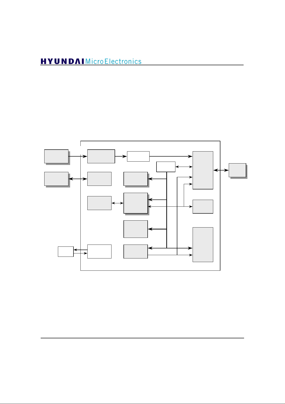
4. Block Diagram
The figure 2 shows the internal block diagram of
the GDC21D301A. This chip receives the byteparallel/bit-serial transport data from
FEC(Forward-Error-Correction) device, and stores
the whole data into DRAM. After decoding the
transport data in DRAM, it de-multiplexes audio,
video, and auxiliary data packets, and transfers
them into the corresponding decoder devices
Transport
FEC
Decoder
8/16bit
8/16bit
MCU
MCU
Stream
FEC
Interface
Host
Interface
TS Buffer
Sync
Detect
GDC21D301A
through the decoder interface blocks. The host
processor can control the GDC21D301A and
access the decoder devices and DRAM through the
host interface. The GDC21D301A generates PWM
pulses to control the frequency of system clock and
audio clock. The pulse width of PWM can be
programmed by the host processor.
Buffer
Memory
Controller
4Mb
DRAM
TS Header
Decode
Adaptation
Field
Decode
PES
Decode
High-speed
Interface
External
Decoder
Interface
VCXO
PID
Memory
Clock
Control
Figure 2. The Block Diagram of the Transport Decoder
12
 Loading...