

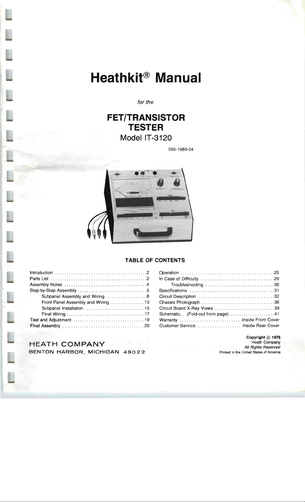
Heathkit@ Manual
for the
FET/TRANSISTOR
TESTER
Model IT -3120
595-1989-04
• • -
'':It
TABLE OF CONTENTS
Introduction ...... . . ......................... . ...
..
Parts List . . .
Assembly Notes
Step-by-Step Assembly
Subpanel Assembly and Wiring . .
Front Panel Assembly and Wiring
Subpanel Installation
Final Wiring
Test and Adjustment
Final Assembly .........
HEATH
BENTON
.......
COMPANY
HARBOR,
. . . ... .
..
........
.....
...........
.. . ..
..
.. . ......... . ..
... . ..... . ......
. . .
......
........
... . ..... . ..
. .
..
...
. . .
.....
. .
..
. . . . . . .
.....
MICHIGAN
. .
........
...
. . .
..
. .
..... . .. . ..
......
. . .
..
..
. . .
...... . ..
. . . .
.. . ....
. . .
..
... . ....
....
. .
..
.....
. .
.......
49022
....
2
Operation
2
In
Case
....
.4
...
..
5
Specifications .. . ..........
. .
..
.8 Circuit Description
.
.19
. . 20
Chassis Photograph
13
15 Circuit Board X-Ray Views
17 Schematic
Warranty
Customer Service
......
of
Difficulty . . ......
Troubleshooting
...
(Fold-out from page) .
.........
.. ...
................ ........
.....
. . . . . . . . . . . .........
...
. .
....... . .....
. . . ... . .
.......
...
. . . .
..
. . . . .
......... . .. . ...
....
..
.. . ..
.. ..............
. .
... . ..........
Printed
..
in
. .
.....
20
29
.......
..
..
...
. . . . .
©
30
.
31
32
. .
38
. .
39
41
.
.
1976
..
.. . .......
......
. . . .
...... . .....
. .
......
. .
.....
. .
....
. .
..
..
.........
...
Inside Front Cover
..
Inside Rear Cover
Copyright
Heath Company
All Rights Reserved
the United States of America
Page
2
INTRODUCTION
The Heathkit Model IT -3120 FET /Transistor Tester
instrument for quick, accurate tests of conventional (bipolar)
transistors, diodes, FET's, SCR's, triacs. and unijunction
transistors. Gain (DC Beta), transconductance (Gm), and
leakage values are read directly
meter.
You
can
quickly
out-of-circu it. The Tester provides special
balance
coded
FET sockets
Five current
microampere and collector currents
out
leads
and easily test devices either in-circuit
in-circuit impedances.
for
in-circuit tests
for
out-of-circuit tests.
ranges
permit
on
the large easy-to-read
Use
or
the
built-in
leakage measurements
as
high
is
a quality
circuitry
either the
transistor and
as
low
as
1 ampere.
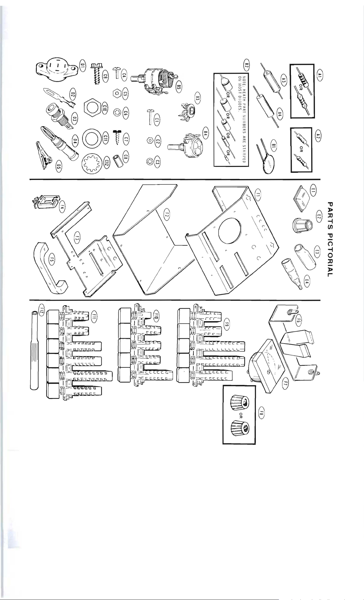
PARTS
Check
each
correspond
from
Page
Any
part
on
it
should
identified
KEY
HEATH
No. Part No.
part against
to
the numbers on the
5) .
that
is
packaged in
be
until
that
PARTS DESCRIPTION
Per
the
following
an
placed back in its envelope after
part
is
called
Kit
list. The key numbers
Parts
Pictorial
envelope
for
with a part
in a step.
(fold-out
or
to
color
as
1
number
it
is
type
Pushbutton
easy,
consistent operation.
A special battery testing
of
the
condition
Another convenience
two-color
conventional (bipolar) transistors and
FET's. Also, separate, brief operating instructions
printed on the rear panel.
Refer
to
the
wiring,
soldering,
range, mode, and
of
front
panel design, black lettering
"Kit
Builders
resistors, and
circuit
the
of
this portable instrument
Guide" for
function
provides a meter indication
self-contained power supply .
capacitors.
switches
red
lettering
information
assure
is
the
on tools,
LIST
To
order a replacement part,
furnished
"Replacement Parts" inside the rear cover
For pricing information, refer to separate "Heath Parts Price
List."
KEY
No. Part No.
with
HEATH
this
kit. If
PARTS
Per
Kit
CAPACITORS-DIODE-CONTROLS
use
the Parts Order Form
one
is
not
DESCRIPTION
available,
of
the Manual.
for
for
are
see
RESISTORS
1/2-Watt
A1
1-129
A1
H05
6-1509
A1
1/4-Watt,
A2 6-1
A2
A2
660-12
6-3600-12
6-1501-
Other
A3 2-11-2
A4 3-13-3
1%
Precision
12
3
4.7
violet-gold)
10
black-orange)
15
green-black-gold)
n,
10% (yellow-
kn,
5%
(brown-
n. 1% (brown
81
82
83
84
85
'
21-57
57-65
10-934
10-926
14-
11
2
.005
J-lF
disc capacitor
1 N4002 silicon diode
750 n control
kn
control
15
250
kn/5000
control
n (5
k)
HARDWARE
#2
166 n
2
(brown-blueblue-black)
360 n (orange-blue
black-black)
1500 n (brown-greenblack-brown)
n,
2-watt, precision
1.5
n.
3-watt,
.15
Hardware
C1
C2
C3
#4
Hardware
C4
C5
C6
250-1'75
252-51
254-7
250-52
252-2
254-9
10
10
10
2-56 x
3/8"
screw
2-
56
nut
#2
lockwasher
1/4"
8
8
8
4-40 x
4-40
#4
lockwasher
screw
nut
I§
~
fUitSf§hi9
Page
3
KEY
No.
-----
#6
Hardware
C7
C8
#10
C9
HEATH
Part No.
250-155
255-49
Hardware
250-83
PARTS DESCR IPTION
Per
Kit
---
6
3
2
#6 x 3/8"
metal screw
#6
# 1 0
self-tapping screw
sheet
spacer
x 1/2" hex head
Control Hardware
C10
C11
C12
252-7
253-10
254-4
2
2
2
Control nut
Control flat washer
Control lockwasher
SOCKETS - JACKS - PLUGS
01
434-342
434-343
02
436-11
03
'03 436-22 Black banana jack
436-24
03
03
436-29
D4 438-47
05
260-53
2
9
1
4
4
Transistor socket
Socket pin
Red banana jack
White banana jack
Green banana jack
Banana plug
Alligator clip
FEET-KNOBS-INSULATORS
E1
261-49
E2
462-362
E3
70-10 Black banana plug
E3
70-11
E3
70-12
E3
70-13
E4
73-34
8
2
4
Rubber
Knob
insulator
Red
insulator
Green banana plug
insulator
White banana plug
insulator
Rubber insulator
foot
banana plug
KEY
HEATH
No. Part No.
~-
-
--
Wire
(cent'd.l
344-70
344-71
344-72
344-73
344-74
344-75
344-77
344-78
PARTS DESCRIPTION
Per
Kit
White-black
White-brown
White-red
White-orange
White-yellow
White-green
White-violet
White-gray
MISCELLANEOUS
85-1167-1
F1
203-1412-2
F2 90-561-3
F3
204-1837
F4
207-82
F5 211-15
F6 214-76
F7
407-173
F8
455-50 2
F9
64-97
F10 64-98
F11
64-99
F12 490-5
597-260
597-308
391-34
The
following
use
in
the
completed
2 O-cell flashlight batteries (alkaline
longer
life).
5
2
1
batteries should
Kit:
Circuit board
Front panel
Cabinet shell
Subpanel
Clamp
Handle
Battery holder
Meter
Knob bushing
Mode switch
Range switch
Function switch
Nut starter
Parts Order Form
Kit Builders Guide
Blue and white label
Manual (See front cover
for part number.)
Solder
be
purchased
type
at
this time
preferred
for
for
WIRE
341-1
341-2
341-5
341·6
344-50
344-51 Brown
344·52
344-54
344-55 Greer.
344-59
Black stranded
Red
stranded
White stranded
Green stranded
Bla.::k
Red
Yellow
White

Page
4
=
= :
1.
Before
have read
the " Kit
2. Resistors
n,
or
kn,
directed otherwise.
starting
Builders
will
to
the
wiring and
Guide."
be
called
and color code.
ASSEMBLY
assemble
out
this
kit. be
soldering
by their respective value in
Use
1/2-watt resistors unless
sure
information
you
in
NOTES
3.
Capacitors
(in
11F)
SAFETY
excess
the
leads.
leads
WARNING:
so
and
We
the
ends
will
be
called
type (disc).
Avoid
suggest
that
will
you wear
not
fly
out
by their capacitance value
eye
injury
when you clip
glasses,
toward
your
or
at least clip
eyes.
off
1"
I I
2"
3"
I
4"
I
5"
I
6"
I
~
~fh*iifHfj]
Page
5
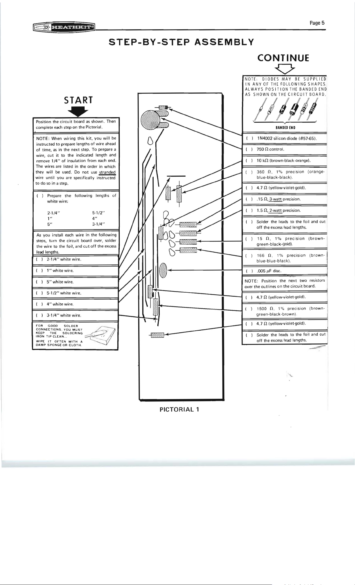
STEP-BY-STEP
START
Position
the
complete each
NOTE: When wiring this kit, you will be
instructed
of time,
wire,
remove
The wires are listed
they will be used .
wire until you are specifically instructed
to
do so
( ) Prepare
As
steps, turn
the
lead
circu it board as shown. Then
step
on
the
to
prepare lengths of wire ahead
as
in
the
cut
1/4"
in
white wire;
1/4"
2·
1"
5"
you install each wire
wire
next
it
to
the
indicated length
of insulation from each end.
in
the
Do
a step.
the
following lengths of
the
circuit board over, solder
to
the
foil, and
Pictorial.
step. To prepare a
order
not
use
in
the following
cut
off
in
~
5·1/2"
4"
3·1/4"
the
and
which
excess
ASSEMBLY
CONTINUE
NOTE
DIODES MAY
I
NAN
Y 0 F
THE
POS
ALWAYS
AS
SHOWN
Il
, v '
750 n control.
10
360
blu
4.7 n (Yellow-violet-gold).
.15
1.5
Solder the leads
off
15
( )
green-black-gold)
166
ITION
ON
lrlll
BANDED
1 N4002 silicon diode
kn
(brown-black-orange).
n.
1%
e-black-black)
n, 3-watt
n,
2-watt precision.
the
excess lead lengths.
n.
1%
n.
F 0 L
THE
CIRCUIT
precision
precision.
precision
LOW
THE
END
.
to
.
BE
the
SUPPLIED
IN
G S HAP E S.
BANDED
BOARD.
(#57-65).
(o
range
foil and
(brown-
(brown-
END
·
cut
I'
1"
white wire.
5"
white wire.
5·1/2"
white
4"
white wire.
3·1/4"
white wire.
rOR
GOOD
CONNECTIONS , YOU
K(EP
~~:
DAMP
SOLDER
THE
SOLDERING
TII~
c~~~:~.
SPONGE
OR
wire.
MUST
WITH
A -. _ _~ I
CLOTH
.
4tl
..
~"
PICTORIAL
1
over
the
outlines
on
4.7 n (yellow·violet·gold).
1500
n. 1%
green-black-brown)
4.7 n (yellow·violet-gold).
the
Solder
off
the excess lead lengths.
the
precision
leads
circuit board.
(brown-
.
to
the
foil and
cut
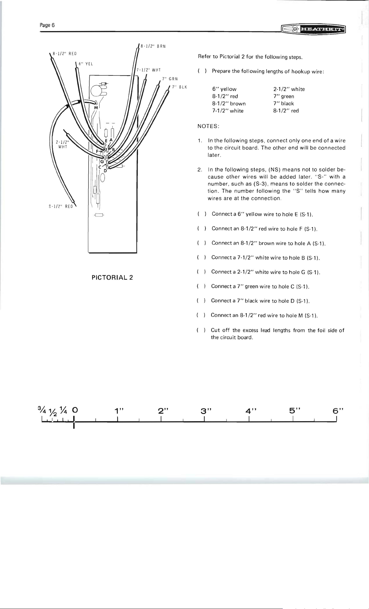
_pa_g_e_6
______________________________________________________________________
Refer
to
Pictorial 2
yellow
the
the
.
the
The
the
red
brown
white
following
circuit
following
other
such
number
are
at
( ) Prepare
6"
8-1/2"
8-1/2"
7-1/2"
NOTES:
1.
In
to
later
2. In
cause
number,
tion.
wires
for
the
following
following
steps,
board. The
steps,
wires
will
as
(S-3),
following
the
connection.
~~~fifi6Sfff{¥~
steps.
lengths
connect
2-1/2"
7"
7"
8-1/2"
other
(NS)
be
added
means
of
hookup
white
green
black
red
only
end
means
to
the
"S"
one
will
not
later.
solder
tells
wire :
end
be
connected
to
solder
"S-"
the
how
of a wire
be-
with a
connec-
many
PICTORIAL
2
Connect a
Connect
Connect
Connect a 7
Connect a
Connect a
Connect a
Connect
Cut
the
an
an
an
off
the excess lead lengths
circuit
6"
yellow
8-1/2"
8-1/2"
-1/2"
2-1/2"
7"
green
7"
black wire
8-1/2"
board.
wire
red wire
brown
white
white
wire
red
wire
to
hole E (S
to
hole
wire
to
wire
to
hole
wire
to
hole
to
hole C (S-1).
to
hole 0 (S-1).
to
hole
-1).
F (S-1).
hole A (S-1).
B (S-ll.
G (S-1).
M (S-1).
from
the foil side
of
34% % 0
I , I I I 1 I
1"
I
2"
I
3"
I
4"
I
5"
I
6"
,
///1
~
..
fU=.MiifH£§l
_____________________________________
• • • • • • • • • •
• • • • • • • • •
• • • • • • • •
• • • •
• • • • •
..
,'
w...
~
..-..
: ,-,-, .
./
-..
'.~
..
.
_ .
JIll...
~,
f18c.
..
"
,'.
-'
""'
....
..
~
J""\
.
.
..
."
.:
....
'..
~
g
P_a_
e_7
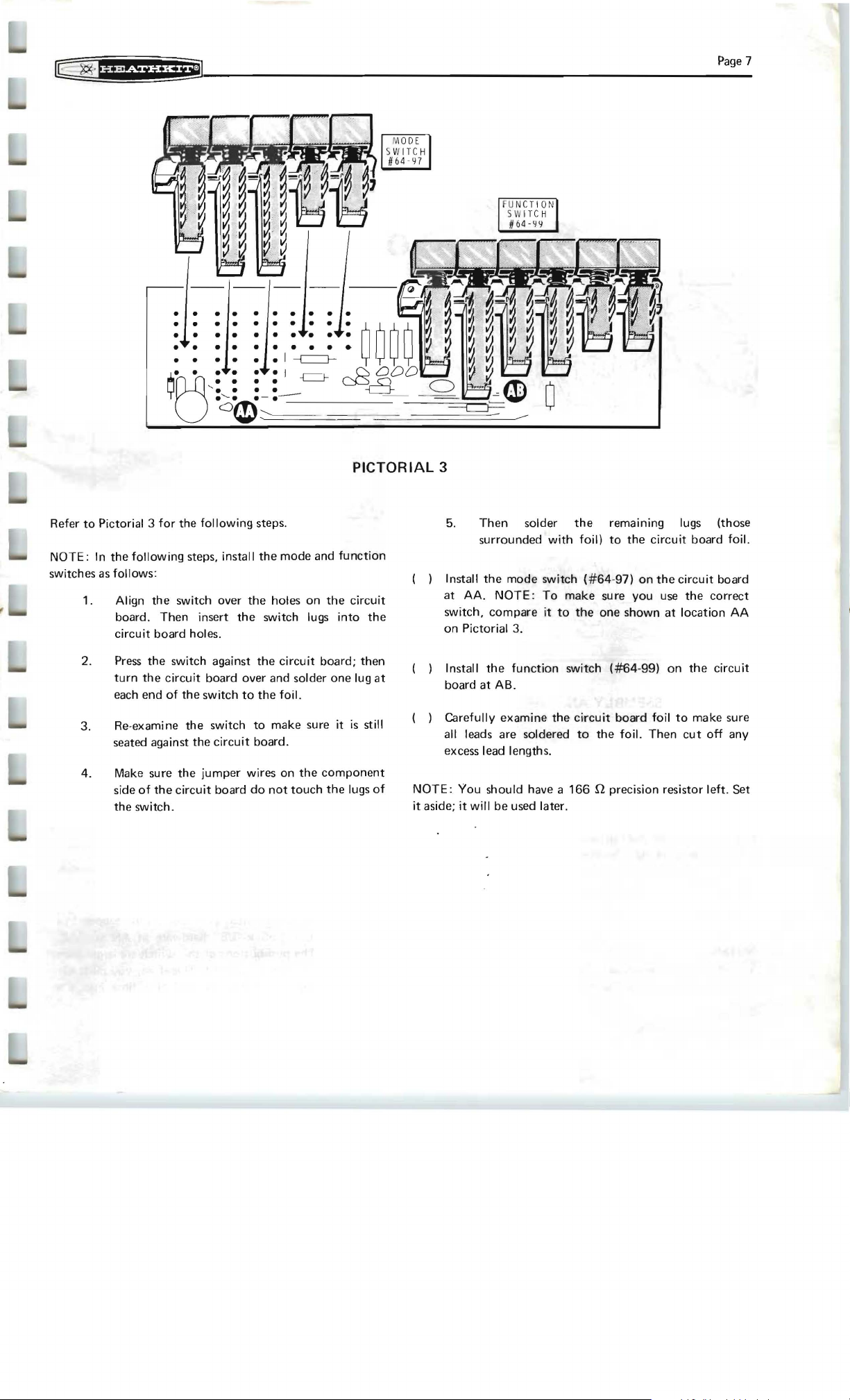
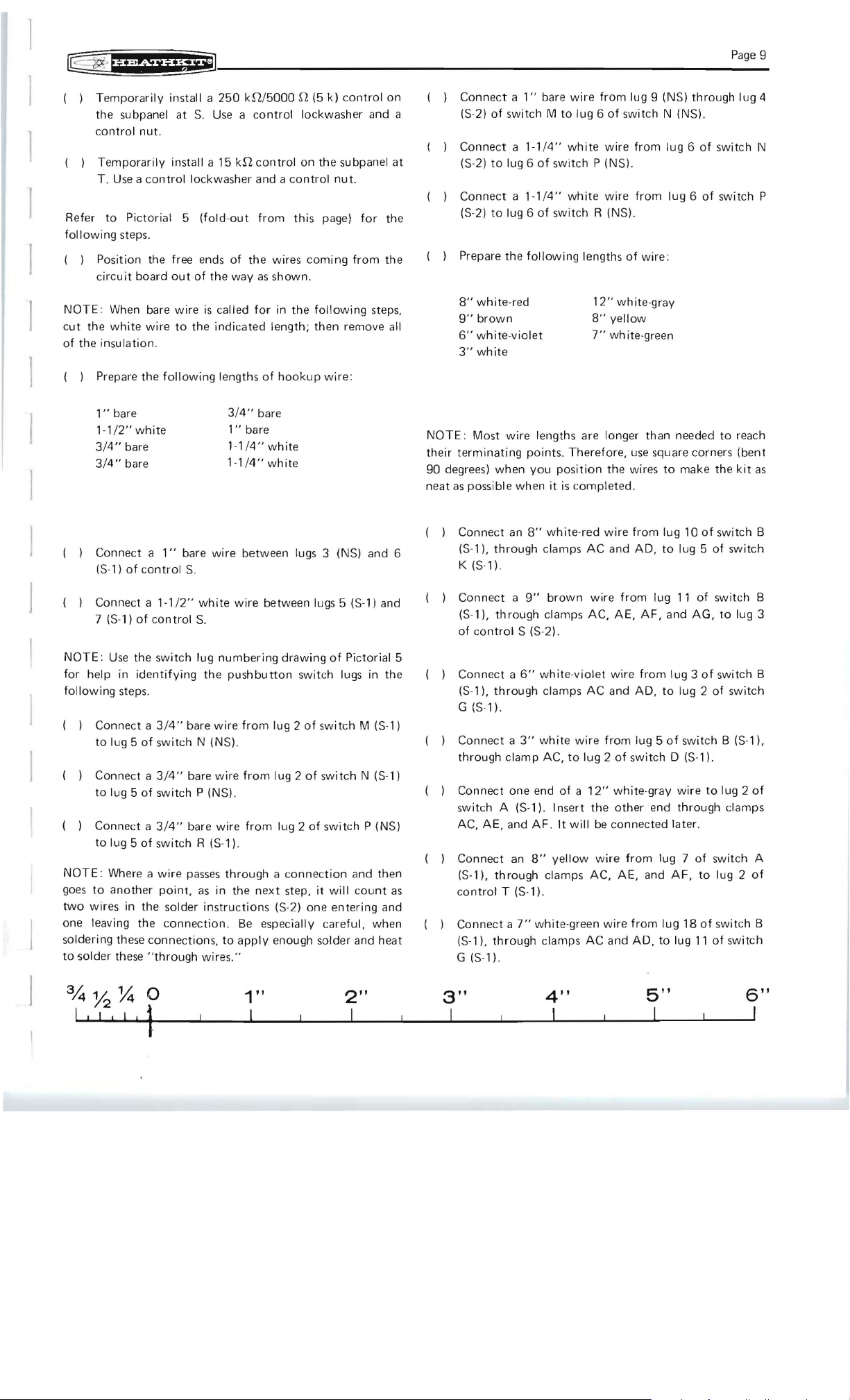
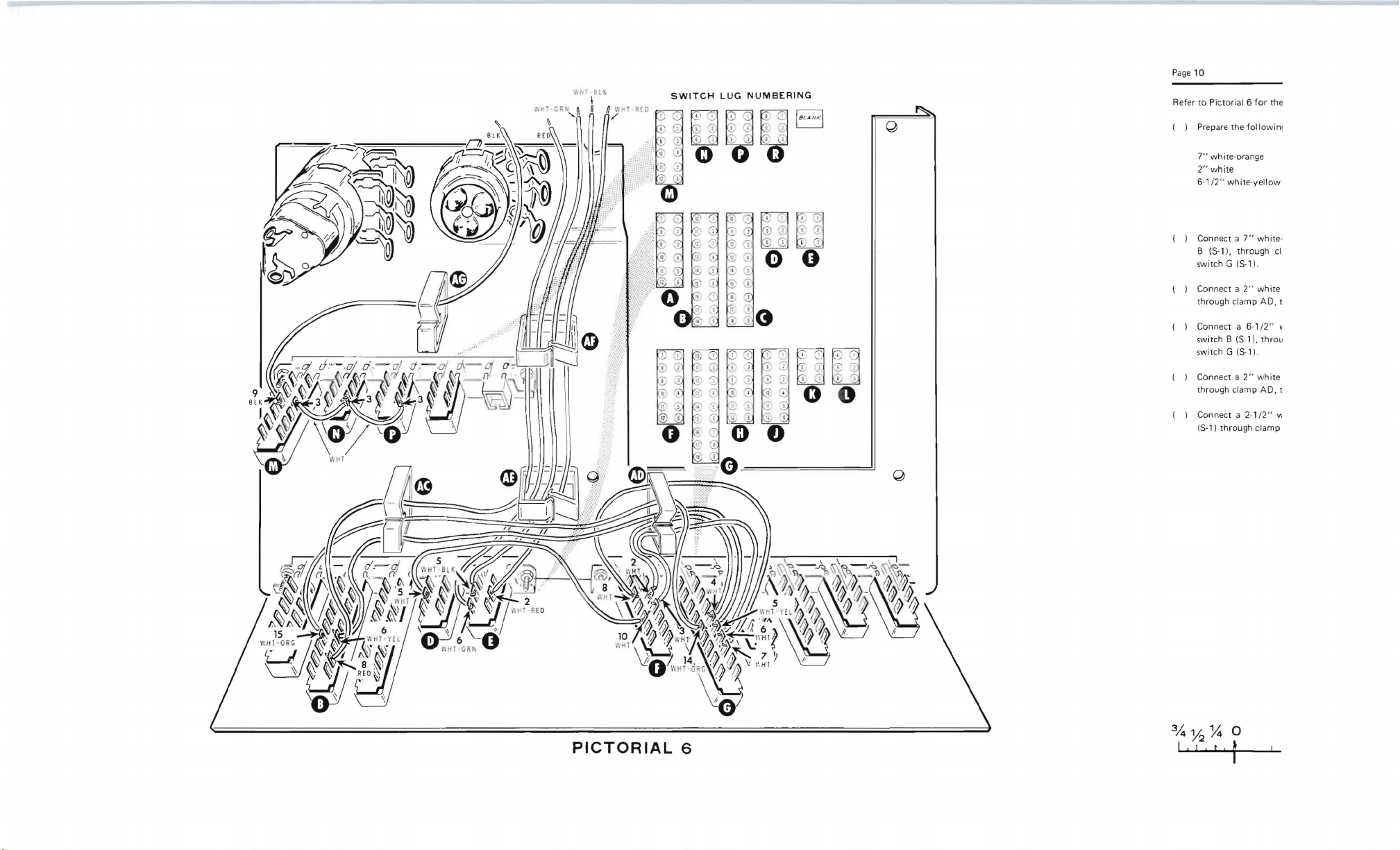
Refer
to
Pictorial 3 for
In
the
NOTE:
switches as follows:
1. Align
2. Press
3.
4.
following steps, install
board.
circuit board holes.
turn
the
each
end
Re-examine
seated against
Make sure
side
of
the
switch.
r..: : ::
YerQ~~:--_?8--
the
following steps.
the
switch over
Then
insert
the
switch against
circuit board over and solder
of
the
switch
the
switch
the
the
jumper wires on
the
circuit board
:
::
the
mode
the
holes
the
switch lugs into
the
circuit board;
to
the
foil.
to
make sure it
circuit board.
do
not
~
and
on
the
touch
cB
oaa
PICTORIAL 3
fu
nction
the
circuit
the
then
one
lug
at
is
still
component
the
lugs
of
~
~
. .
~~
Then
5.
surrounded
the
Install
at
AA. NOTE: To make sure you use
switch,
on
Install
board
Carefully
all
excess lead lengths.
NOTE:. You should have a
it
aside; it will
compare
Pictorial 3.
the
at
AB.
examine
leads
are
be
0
solder
with foil)
mode
switch
it
function switch
the
soldered
used later.
to
166
the
(#64-97)
the
circuit
to
remaining lugs (those
to
the
circuit board foil.
on
the
circuit board
the
correct
one
shown
at
(#64-99)
board foil
the
foil.
on
Then
location
the
to
cut
AA
circuit
make sure
off any
n precision resistor left. Set
Page
8
:::
o
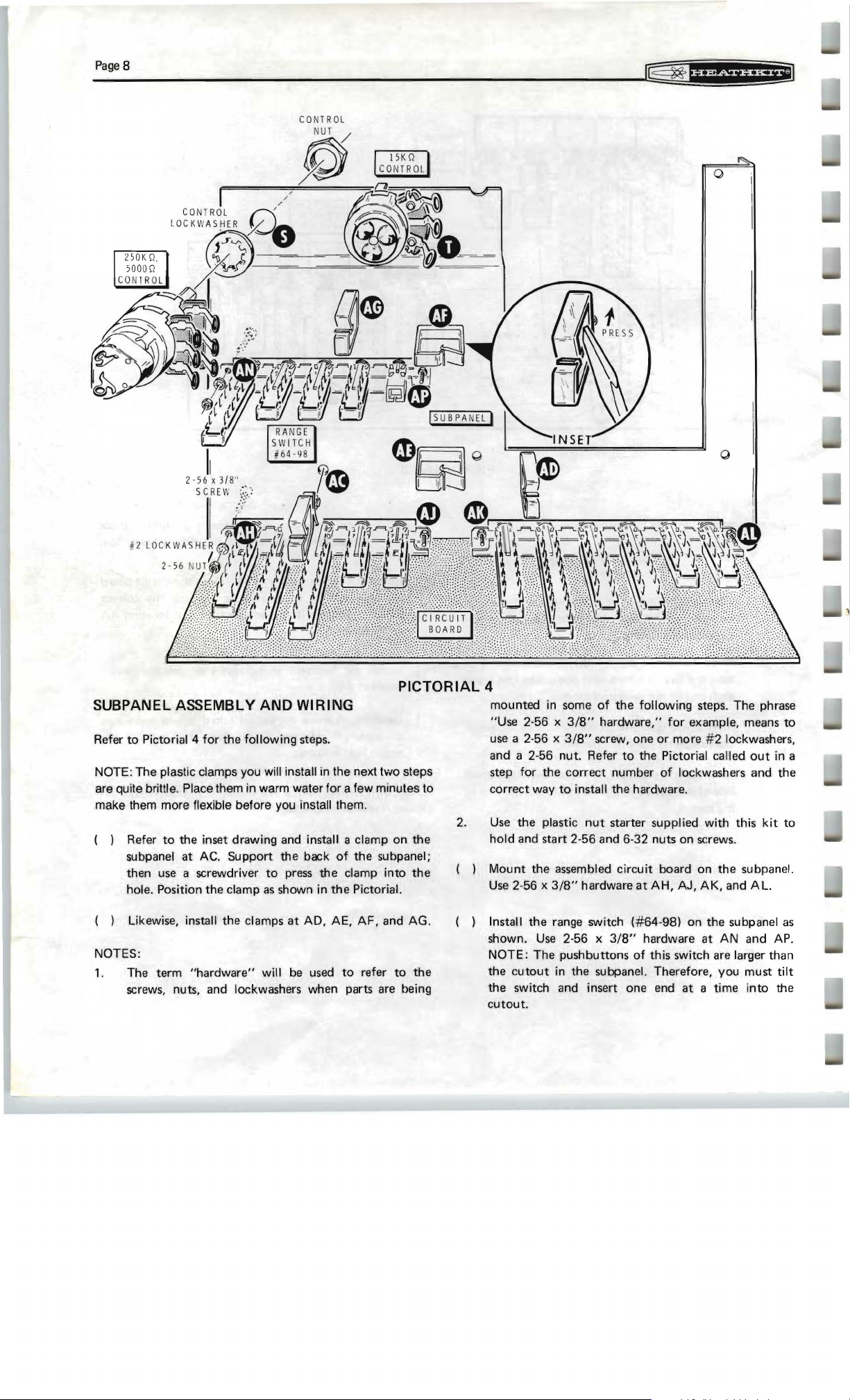
PICTORIAL 4
SUBPANEL ASSEMBLY AND WIRING
Refer
to
Pictorial 4
NOTE: The plastic clamps you will install in the next two steps
are quite brittle. Place them in warm water
make them more flexjble before you install them.
( ) Refer
subpanel at AC. Support the back
then
use
hole. Position the clamp
( ) Likewise, install the clamps
NOTES:
1. The term
screws, nuts, and lockwashers when parts are being
for
the
following
to
the inset drawing and install a clamp
a screwdriver
"hardware"
to
press
as
shown in
at
will
steps.
AD, AE,
be
used
for
a few minutes to
of
the clamp
the
to
on
the
the subpanel;
into
the
Pictorial.
AF,
and AG .
refer
to
the
of
the
mounted in some
"Use 2-56 x
use
a 2-56 x
and a 2-56 nut. Refer
step
for
correct way
2.
Use
the plastic
hold
and start 2-56 and 6-32 nuts on screws.
( )
Mount
Use
2-56 x
( ) Install the range switch
shown.
NOTE:
cutout
the
the switch and insert one end at a time
cutout.
3/8"
3/8"
screw, one
the
correct
to
install the hardware.
nut
the assembled
3/8"
hardware
Use
2-56 x
The push
buttons
in the subpanel. Therefore, you must
following
hardware,"
or
to
the Pictorial called
number
starter suppl ied
circuit
3/8"
of
board on the subpanel.
at
AH,
(#64-98)
hardware at
of
this switch are larger than
steps. The phrase
for
example, means
more
#2
lockwashers,
out
lockwashers and the
with
this
kit
AJ,
AK,
and
AL.
on the subpanel
AN
and AP.
into
to
in a
to
as
tilt
the
_p_ag_e__1_0
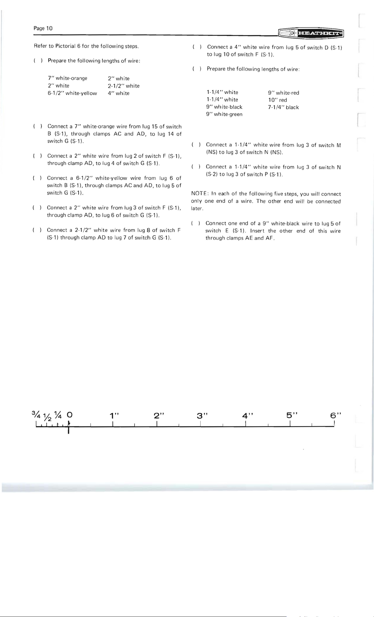
Refer
to
Prepare the
7"
2"
6-1/
_____________________________________________________________________
Pictorial 6
white-orange
white
2"
for
the
following
white-yellow
following
lengths
2"
white
2-1 /2"
4"
white
steps.
of
white
wire:
( )
Connect a 4"
to
lug
( ) Prepare
1-1/4"
1/4"white
1-
9"
white-black
9"
wh
10
of
switch F (S-1).
the
following
white
ite-green
wh
ite
wire
lengths
9"
10"
7-1 /4"
~
from
white
red
fifPhSiifi¥£iU
lug 5
of
switch D (S-
of
wire:
-red
black
1)
Connect a
B
(S
switch G (S-1).
( ) Connect a
through clamp
( ) Connect a 6-1/
switch B (S-1), through clamps
switch G (S-1).
( ) Connect a
through
Connect a 2-1/
(S-1)
-1).
through
clamp
through
7"
white-orange
2"
white
AD.
2"
2"
white wire
AD,
2"
cla
mp
wire
clamps
white
AC
wire
from
to
lug 4
of
white-yellow
from
to
lug 6
of
wire
AD
to
l
ug 7 of
from
lug 15
and AD.
lug 2
switch G (S-1).
wire
AC
lug 3
switch G (S-
from
to
of
switch F (S-1)
from
and
AD,
to
of
switch F (S-1) ,
1)
lug 8
of
switch G (S-1).
of
switch
lug 14
lug 6
lug 5
.
switch F
of
.
of
of
only one end
later .
( )
( )
Connect
(NS)
( )
Connect
(S-2)
NOTE
: In each
Connect
sw itch E (S-1).
through
to
to
lug 3
a 1-
lug 3
of
one end
clamps
a 1-1/
4"
of
switch
1/4"
of
switch P (S
of
the
following
a w ire. The
AE
white
white
of
a 9"
Insert
and
wire
N (NS).
wire
-1).
fiv
other
white
the
AF.
from
lug 3
from
lug 3
e steps,
end
will
-black wire
other
end
of
switch M
of
switch
you
will
connect
be connected
to
lug 5
of
this
N
of
wire
3,4
% % 0
~1~,~I~,~t~,~~----L---~I~--~--~I----~--~1
1"
2"
3"
____
L-
___
4"
!L-
I
5"
__~__~!____~___
6"
,
~ >fif=f§fiif{~
_______________________________________________________________________
pa
_g_e_9_
( )
Temporarily
su
the
control
( )
Temporarily
T.
Use a control
to
Refer
following
( ) Position the free ends
NOTE:
cut
of
the insulation.
( ) Prepare the
Pictorial 5 (fold-out
steps.
circuit
When bare
the
white
1"
bare 3/
1-1/2"
3/4"
bare
3/4"
bare
install a
bpanel at
nut.
install a 15
board
out
wire
wire
to
following
white
S.
lockwasher and a
of
the way
is
the
250
kD/5000
Use a control
kD
control
from
of
the wires
as
shown.
called
for
in the
indicated
lengths
1"
1-1/4"
1-1/4"white
4"
bare
length;
of
bare
white
hookup
D (5
k)
control
lockwasher and a
on the subpanel
control
nut.
this
page)
coming
following
then remove all
wire
:
for
from
on
the
the
steps,
at
( )
( ) Prepare the
NOTE:
their
90 degrees)
neat
Connect a 1"
(S-2)
of
switch M to
Connect a 1-1/4"
(S-2)
to
lug 6
of
Connect a 1-1/4"
to
lug 6
(S-2)
8"
white-red
9"
brown
6"
white-violet
3"
white
Most
terminating
when
as
possible when
of
following
wire
lengths are longer than needed
points.
you
bare
switch
switch
position
it
is
wire
from
lug 6
of
white
wire
P (NS).
white
wire
R (NS).
lengths
12"
8"
yellow
7"
wh
Therefore,
the wires
completed.
lug 9 (NS)
switch
N (NS).
from
lug 6
from
lug 6 of
of
wire:
white-gray
ite-green
use
square corners (bent
to
make the
through
of
switch
switch
to
lug 4
reach
kit
as
N
P
( )
Connect a 1"
(S·l)
of
( ) Connect a
7
(S-l)
of
NOTE:
for
following
( )
( ) Connect a
( ) Connect a
NOTE
goes
two
one leaving the
soldering these connections,
to
Use
the
help in
to
wires in the solder
solder
identifying
steps.
Connect a 3/4"
to
lug 5
to
lug 5
tolug50fswitch
: Where a
another
these
bare
control
of
of
S.
1-1/2"
white
con
trol
S.
switch
"through
lug
bare
switch
N (NS).
3/4"
bare
switch P (NS).
3/4"
bare
R
wire
passes
point,
as
connection . Be
the
instructions
wires."
wire
between lugs 3 (NS) and 6
wire
between lugs 5
numbering
pushbutton
wire
wire
wire
(S-l).
through a connection
in
the
to
apply
drawing
switch lugs in the ( )
from
lug 2
of
swi tch M
from
lug 2
of
switch N (S-l)
from
lug 2
of
switch
next
step,
it
(S-2) one
especially
enough solder and heat
careful,
(S-l)
of
Pictorial 5
P (NS)
and then
will
count
entering
and
(S-l)
as
and
when
( ) Connect an
(S-l),
K
(S-l).
Connect a 9"
(S-l),
of
control
Connect
(S-l),
G
(S-l).
Connect a 3"
through
( ) Connect one end
switch A
AE,
AC,
Connect
( )
(S-1),
control T (S-l)
Connect
( )
(S-l),
G
(S-l).
8"
through
through
S (S-2).
a
6"
through
clamp
(S-l).
and
an
through
a
7"
through
white-violet
white
AF.
8"
.
white-green
clamps
white-red
clamps
brown
clamps
clamps
wire
AC,
to
lug 2
of a 12"
Insert the
It
will
yellow
clamps
wire
from
AC
and
AD,
wire
from
AC,
AE,
AF,
wire
from
AC
and
AD,
from
lug 5
of
switch D (S-l).
white-gray
other
be
connected later .
wire
from
AC,
AE,
wire
from
AC
and
AD,
lug
end
and
lug
to
lug 5
11
and
lug 3
to
lug 2
of
wire
through
lug 7
AF,
lug 18
to
lug
10
of
switch
of
switch
of
switch
AG,
to
lug 3
of
switch
of
switch
switch B (S-l),
to
lug 2
of
clamps
of
to
of
11
switch
of
lug 2
switch
switch
A
of
B
B
B
B
1"
I I
2"
3"
I
4"
I
5"
I
6"
I
Page
n lug 9 (NS) through lug 4
,witch
N (NS).
from
lug 6
of
lug 6
switch N
of
switch P
'e
5)
-e
from
5)
;
of
wire :
Nhite·gray
,
II
ow
hite-green
9
SWITCH
LUG
NUMBERING
Q
'ger than needed
~
.
us
e square corners (bent
?
INires
to make the kit
,d.
-e
from
lug
,d
AD.
to
from
lug
AF,
IE,
ire
from
AD,
to
,d
m lug 5
sw
itch D
.f
,hi Ie-gray wire
ther end through clamps
mnected late
from
lug 7
>.E,
and
e
from
lug
dAD,
10
to
lOaf switch
lug 5 of switch
11
of
swi tch B
and AG,
to
lug 3
of swit
lug 2 of switch
of
switch B (5·11,
(5·1
J.
to
lug 2
r.
of
switch A
AF,
to
lug 2
18
of switch
lug
11
of
reach
lug 3
ch B
switch
as
B
Q
of
of
B
PICTORIAL
5
5"
I I
6"
wH"
-eRN
~
IIhT \
SlK
~
R n\'lhT R[D
'n
n n/ I
Pi
SWITCH
LUG
NUMBERING
Q
Page
10
Refer
to
Pictorial 6
( ) Prepare the
7"
white-orange
2"
white
6-1
/2"
white-yellow
)
(
Connect a
B
(5-1),
switch G (5-11.
)
(
Connect a
through clamp
)
(
Connect a
swil
ch
B (5-1),
switch G
( )
Connect a
through clamp
( )
Connect a
(5-1) through clamp
for
followin'
7"
white-
through
2"
white
AD,
6-1/2"
throu
(S-l).
2" while
AD,
2-1/2"
the
cl
I
v
t
11\
PICTORIAL
6
Q
%%~O
I I ! t! t !
Refer
to
Pictorial 8
Prepare a
10"
for
the
length
following
of
black solid wire.
steps.
. / 5
OPEN
IDE
Page
13
Connect one end
switch A
through clamps
( ) Route the red wire coming
through clamps AC and
( ) Connect the
hole
T
(S-l).
( ) Connect the black wire coming
hole D, through clamps AE,
switch P (S-2).
( ) Connect the green
hole
switch P (S-2).
( ) Connect the
hole B, through clamps
switch N (S·2).
( ) Connect the brown
hole
switch M
( ) Connect the red wire coming
F, through clamps
M (S-1).
( ) Connect the
hole G
( ) Refer
each
arm
This completes the assembly and
it
aside temporarily.
(S-l).
E,
through clamps
C,
through clamps
A,
through clamps
(S-l).
to
lug 3
to
the
clamp.
until
it
locks
of
a
10"
black wire
Insert
the
other end
AC
and
AD.
It
will
from
AD.
It
will
yellow
white
white
To
wire coming
AE
and
AF,
AF,
wire
coming
AE,
AF,
wire coming
AE,
AF,
wire
coming
AE,
AF,
from
AE,
AF,
and
AG,
wire coming
of
switch D
inset drawing on Pictorial 8 and close
do
to
(S-l)
.
this, push inward on
the stationary arm.
wiring
FRONT PANEL ASSEMBLY AND
Refer
to
Pictorial 9
Place a soft
( )
front
panel
( ) Locate the
for
the
following
cloth
on
your
from
becoming scratched.
front
panel and position
work
steps.
surface
to
of
be
connected later.
circuit
board hole M
be
connected later.
from
circuit
to
lug 1
from
circuit
and
AG,
to
from
circuit
and
AG,
to
from
circuit
and
AG,
to
from
circuit
and AG,
from
of
WI
it
circuit
to
lug 6
circuit
the
the
subpanel. Set
RING
to
as
shown.
to
board hole
protect
lug
11
this wire
board
of
control
board
lug 2
board
lug 5
board
lug 5
board
lug 8
of
switch
board
flexible
the
of
't
. 1
/
0'
1,
'
C~K
3
~~
;
15
~~~
70
~
Detail 9A
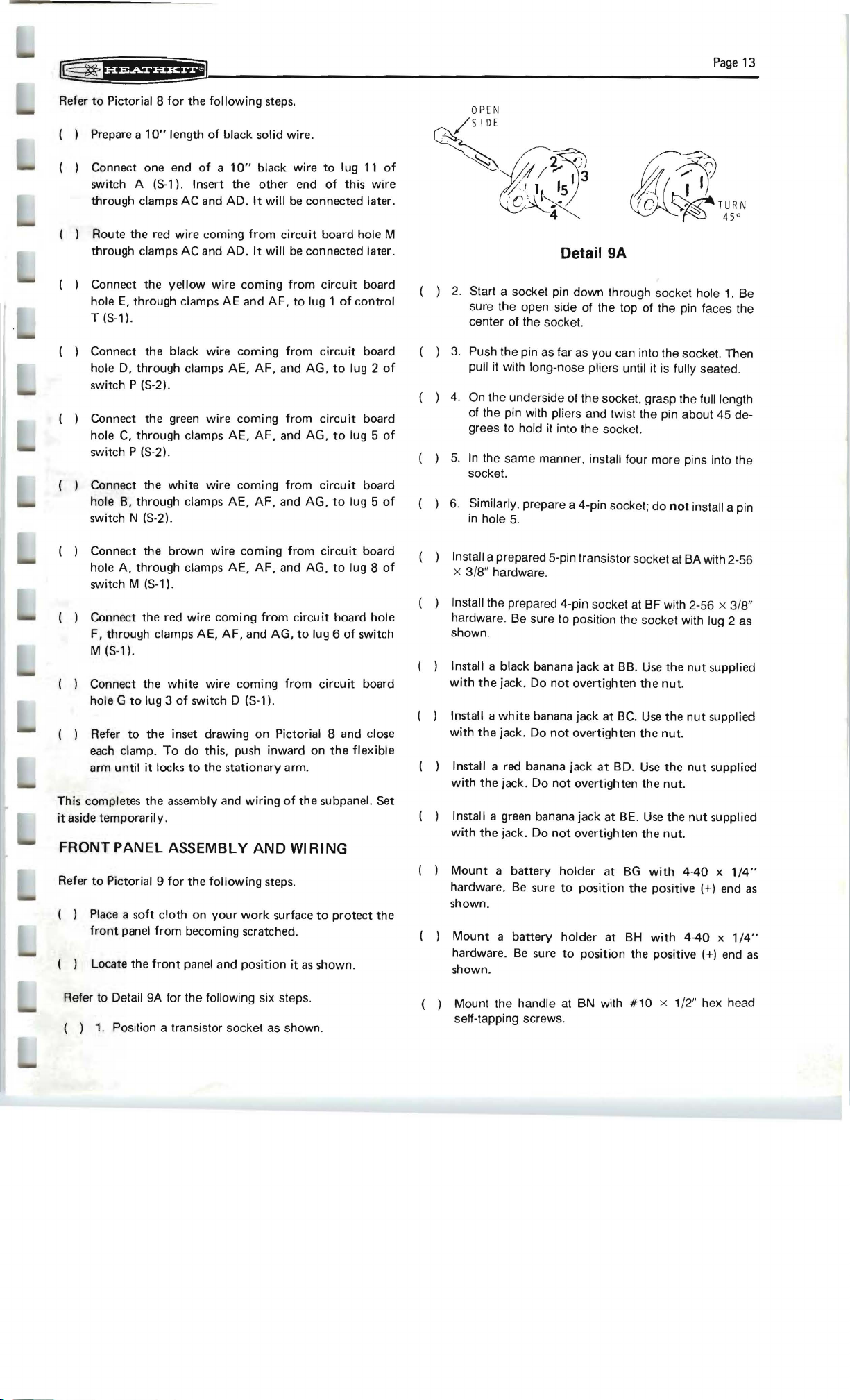
( )
2.
Start a socket pin down through socket hole 1. Be
sure the open side of the top of the pin faces the
center of the socket.
3.
( )
of
( ) 4. On the underside of the socket. grasp the full length
of
( ) 5.
of
( ) 6. Similarly . prepare a 4-pin socket; do
( ) Install a prepared 5-pin transistor socket at BA with 2-56
of
( ) Install the prepared 4-pin socket at BF with 2-56 x 3/8"
( ) Install a black banana jack
( ) Install a
( ) Install a red banana jack
( ) Install a green banana jack at
( )
( )
Push the pin as far as you can into the socket. Then
pull it with long-nose pliers until it is fully seated.
of the pin with pliers and twist the pin about 45 degrees to hold it into the socket.
In
the same manner. install four more pins into the
socket.
in
hole
5.
x 3/8" hardware.
hardware. Be sure to position the socket with lug 2 as
shown.
at
BB.
with
the
jack. Do
white
with
the
jack. Do
with
the jack. Do
with
the jack. Do
Mount a battery
hardware.
shown.
Mount
hardware.
shown.
a battery holder at
not
overtighten
banana jack at BC.
not
overtighten
not
overtighten
not
overtighten the nut.
holder at
Be
sure
to
position the positive (+) end
Be
sure
to
position the positive (+) end
at
BD.
BE. Use
BG
BH
not install a pin
Use
the
the
nut.
Use
the
the
nut.
Use
the
the
nut
the
with
with
'~
TURN
45°
nut
supplied
nut
supplied
nut
supplied
.
nut
supplied
4·40 x 1/4"
as
4-40 x 1/4"
as
'Refer to Detail 9A for the following six steps.
1.
( )
Position a transistor socket as shown.
( ) Mount the handle at BN with
self-tapping screws.
#10
x 1/2" hex head

Page 14
®
~
fH*iifH£il
o
PICTORIAL
o
10
.l
1"
I
2"
I I
3"
4"
I I
5"
6"
I

:;: :;:
Refer
to
Pictorial 10
( ) Prepare the
~
for
the
following
following
lengths
of
steps.
wire:
( ) Cut both
leads
Then connect this capacitor
(NS)
to
the
lug
of
of
jack
a .005
BO
IlF
disc capacitor
from
the lug
(NS).
of
Page
to
jack
15
3/4".
BC
3-1/2"
green
5"
white
5"
white
4"
black
( ) Connect a
(S-1)
tothe
( ) Remove
an
of a 5"
through lugs 2
3-1/2"
white
green
lug
of
jack
additional
1/4"
wire. Connect this end
(S-2)
and 5
socket BA. Connect the other end
BC
(NS) .
( ) Connect a
to
the lug
( ) Connect a
to
the lug
( ) Connect a
to
the lug
Connect a
to
the lug
Connect a
(S-1)
to
5"
of
jack
4"
of
jack
6"
of
jack
4"
of
jack
5-1/2"
the lug
white
wire
BC
(NS).
black wire
BB
(NS).
black wire
BB
(NS).
red wire
BO
(NS).
red wire
of
jack
6"
4"
5-1/2"
wire
BE
from
from
from
from
BO
black
red
from
(NS).
of
insulation
(S-2)
lug 1
lug 3
lug 3
lug 2
from
(NS).
red
lug 4
to
to
of
of
of
of
lug 1
of
socket B F
from
one
end
of
the wire
lug 4
(S-1)
the lug
of
jack
socket BF (S-1)
socket
BA
(S-1
socket
BF
(S-1)
socket
BF
(S-1)
of
socket BA
SUBPANEL
Refer
to
following
( )
Mount
meter
only
included
( ) Place a
INSTALLATION
Pictorial
steps.
the
with
a lockwasher and
11
(fold-out
meter on the
front
the positive (+) terminal
nut
at
with
the meter.
from
Page
panel. Position the
as
BJ.
Use
#6 spacer on meter mounting bolts BK, BL,
and BM.
of
( ) Locate the assembled subpanel and remove the control
nuts
from
controls
Sand
T.
( ) Install the assembled subpanel on the inside
front
panel .
)
( ) Install lockwashers and nuts
the hardware included
pushbutton switches do
panel.
If
necessary, reposition the
( ) Install
controls
()
Remove and discard the shorting wire from between
control
Sand
flat
T.
at
BK,
BL,
with
the meter.
not
bind against the
su
bpanel.
washers and control nuts on
the meter terminals.
17)
for
the
shown. Install
the hardware
of
the
and BM.
Be
Use
sure
front

Page 16
o
o
(
/
o
PICTORIAL
12
o
\
)

[[ ~fffWSi*fl5fj)
Page
17
FINAL
Refer
( ) Connect
Connect
WIRING
to
Pictorial 12 (on
Connect
positive (+)
Connect the black
negative
lug
of
jack
Connect the
lug
of
jack
the
Red
wire
wire
Green
White-red
White
-black
the
(-)
the
wires
to
wire
red
wire
terminal
term
i nal
black
BB (S-3) .
white
BC (S-4).
coming
the
lug
to
the
lug
to
lug 1
wire
to
Page
16)
for
coming
of
the
meter
wire
coming
of
the
meter
wire
coming
wire
coming
from
clamp
of
jack BD (S-4).
of
jack BE (S-2).
of
battery
lug 2
of
battery
the
from
(S-l).
from
from
from
AF
holder
following
clamp
clamp
(S-l).
clamp
clamp
as
follows:
BG
holder
steps.
AD
AD
AG
AG
(S-l).
BG
to
the
to
the
to
the
to
the
(S-l).
IAI
REMO
VE
lEST LE
r-
c~
-
'I
I",
I
THE
AD AII.D TW
3/
4~
;;:»
;:)
sst
I B I I
II:
BA
fl
0
~
:~~l
:
AT
r
_ '
I / PHI LLI
I SC
~/
, PLACE T
t
l
/
'1/8"
I HI E B AN A
-rr
(C
I
IN SERT
INTO
T
HEN INSTALL THE CLI P INSU
~:
''"
''lEO
PS
REWDRIVE
PHI LL IPS SCREWDRI VER ,
TOOl !. PUSH THE
11\5ULATOR SNAPS I N PLACE.
THE OTHER END
THE
ALLIGATOR
INSULA
TIO
I\ I ROM TACH END OF T
I SI T
OGUHER THE FINE WI
0 r 1/4'4
a e
S E R T THE
NANA P
AT AGAI NST THE PLUG BODY.
U
.,"
3/
4" BAR 1 0
LUG
. 8 [ I\D BOl H
IV I RE
WI
G
~
~O]
R -
HE
BANA NA PLUG ON A sr.1
1\
A P
OF
CLI P. SOLD
G
~-~
~
-
-=
- -
OR
I
~SU
IAT
ND \'11 R E
ST LEAD
ER
THE
OR
ON
OR
LU
G A
TH E TE
LAT
/.-d~
CRI M P A
~
I I" T
OT
RE [ N
SIMIL
OV
ER
UN
T IL T
LEA
D.
THE CLI
ND
RES
ALL
AR
HE
OS
.
H E
HE
P.
White·green
White-gray
This
Check
Switches C and L should
to
the switch lugs.
to
Refer
Pictorial 13
Prepare
shown
wire
completes
to
see
the
in Part A
wire
to
lug 1
to
lug 2
the
wiring
that
all
for
the
following
red test lead
of
Pictorial 13 . Then install a banana
of
battery
of
battery
of
your
connections
not
have
steps.
from
holder
holder
BH
Transistor
are soldered.
any
wires connected
red stranded
BH
(S-l).
Tester.
wire
(S-l).
as
~
t
TESTCLIP
INSULATOR
plug
with
clip
and
rubber
lead
as
shown
In a similar manner,
black,
white,
~
__
PICTORIAL
a red
insulator
insulator
in
Parts
and green test leads.
~/
~
13
on one end and an
on
the
Band C of
use
stranded
"
other
end
of
the Pictorial.
wire
and prepare the
alligator
the
test
34
Y2
I , I , I ,
X 0
I
1"
2"
3"
1
4"
1
5"
I
6"
J
Page
18
®
~
fUMeHail
PICTORIAL
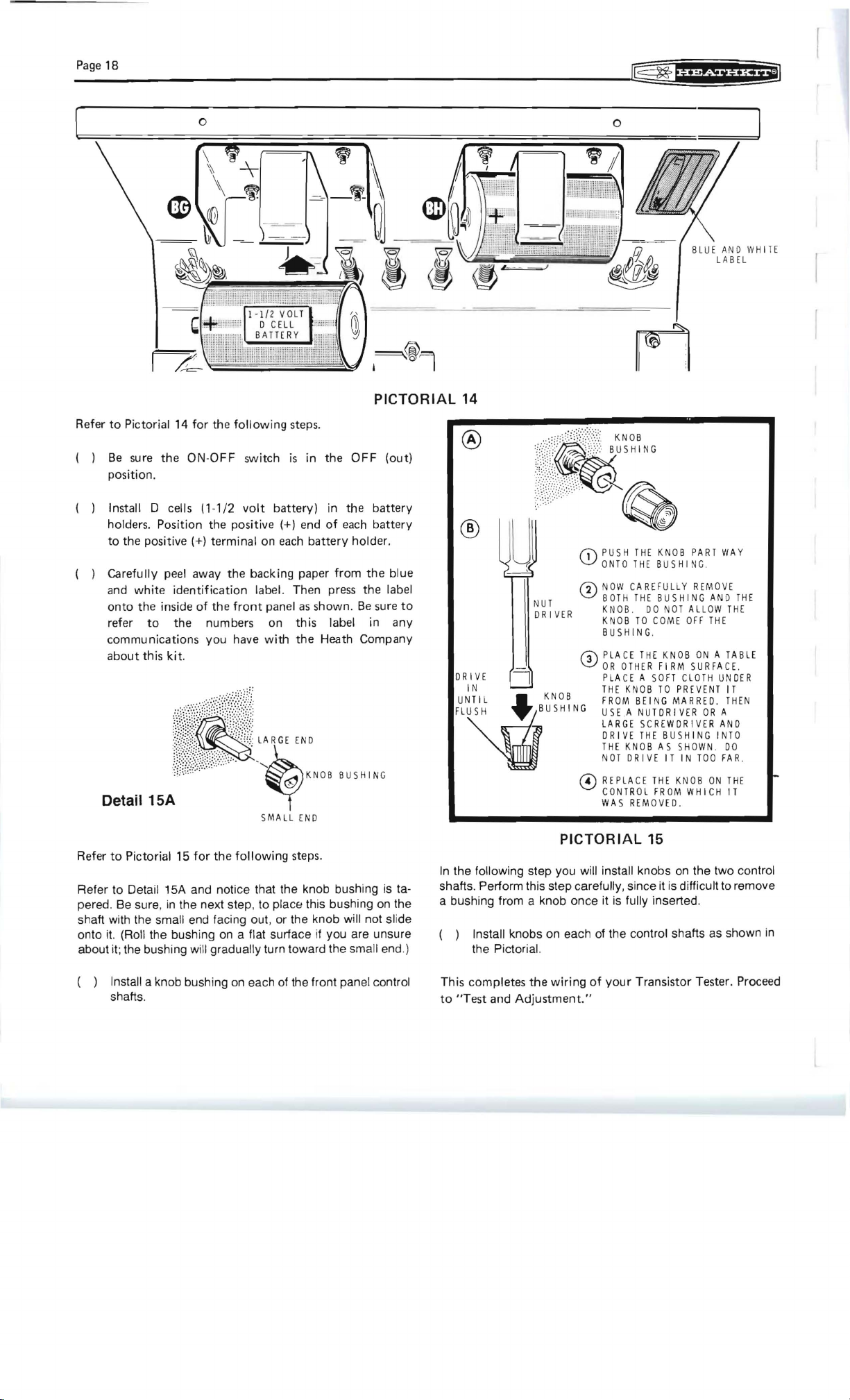
Refer
to
Pictorial
Be
( )
( ) Install D cells
( ) Carefully peel away the backing paper
sure
position.
holders. Position the positive
to
the positive (+) terminal on
and
onto
refer
communications you have
about
14
the
white
identification
the inside
to
the numbers
this
kit.
for
the
following
ON·OFF switch
(1 -1/2
of
the
volt
label. Then
front
panel
with
on
steps.
is
in the OFF (out)
battery) in the battery
(+) end
each
of
each
battery
battery
as
this label in any
the
holder.
from
the
blue
press
the label
shown.
Be
sure
Heath Company
BUSH I
NG
Detail15A
SM ALL
END
Refer
to
Pictorial 15
Refer to Detail
pered . Be sure,
shaft with the small end facing out, or the knob will not slide
it.
onto
about it; the bushing will gradually turn toward the small end.)
(Roll the bushing
for
the
following
15A
and notice that the knob bushing is ta-
in
the next step, to
on
a flat surface if you are unsure
steps.
placE!
this bushing
on
the
14
®
®
f'J\
PUS
H T
HE
KNO B PA
HI
ULLY
TH E BUSHIN
DO
NOT
ALL
ING .
CE
THE
TH
ER
.A NUTDRIVER OR A
SC
THE
KNO
LA
CE T
TR
OL
S REMOVED.
OFF
KNOB
FI
RM
50
FT
CLOTH UNDER
TO
PREVENT
REWDRI V
BUSHING INTO
B AS
SHO
HE KNOB
FR
OM
WHI
15
on
fully inserted .
to
DRI VE
I N
UNTI L
,,~
u
NUT
DR IVER
___
\V
o N
rJ'I
\V
KNOB
m
ING
o REP
ONTO THE BUS
OW CAREF
B
OTH
KNOB .
KNO B TO COME
B
USH
P
LA
OR O
PLACE A
THE KNOB
FR
OM BEI NG MARRED.
USE
RGE
LA
DRIVE
THE
NOT DRIVE I T I N T
CON
WA
PICTORIAL
In
the following step you will install knobs
shafts. Perform this step carefully, since it is difficult to remove
a bushing from a knob once it
( ) Install knobs on each of the control shafts as shown in
the Pictorial.
is
RT WAY
NG
REMOVE
G AND
THE
OW THE
THE
ON A TA BLE
SURFA CE.
I T
THEN
ER
AND
WN . DO
OO
FAR
.
ON THE
CH
IT
the two control
( ) Install a knob bushing
shafts.
on
each of the front panel control
This completes
to
"Test
and
Adjustment."
the
wiring
of
your
Transistor Tester. Proceed

1J
o
-f
o
:IJ
»
r
...
...
--
o
()
---


FINAL
WIRING
Refer
to
Pictorial 12 (on
( ) Connect the red wire
( ) Connect
Connect the
Refer
(+
positive
Connect the black
ve
(-)
negati
the
of
jack BB (5-3).
lug
th
Connect
of
jack BC 15-4).
lug
wi
res coming
Red
wire
wire
Green
White-red
White·black wire to lug 2
White·green wire
White-gray
Thi
s completes
to
Check
Switches C and L should n
to
the switch lugs.
to
Pictorial
Page
) terminal
wir
terminal of the meter (5-1).
black wire coming
e white
wire
to
th e lug
of
to
the lug
wire
to lug 1
to
wire
to
lug 2
the
see
that
13 for
th e fol
16)
for
the
following
steps.
coming
of
from
lug 1
wiring
from clamp
the meter (5-1) .
e coming from clamp
fro
coming
from
clamp
AF
jack BD (5-4) .
of
jack
BE
(5·2).
of
batlery
holder
of
battery
of
battery
of
banery
of your Transist or Tester.
all connections are soldered .
Ot
have any wires connected
lowing
steps.
AD
AD
m clamp AG
clamp AG
as
follows:
BG
holder
holder
holder
BH (5· 1).
(5-1
BG
BH (5·1).
to
to
to
to
).
(5·1).
the
the
the
the
,AI
RfMOv[
Ul£ I " ".
'.H
ATlO""
IISllE~ D
A" O
r-lfL.j 0
1\'/1>
tRO·\' [ACH
,
I
OC.[IHI~
IHE
fiNE ViIRE
ii'
"'==" aI'
,8,
-
' I
I
I",
I
G
hi='
O--
..
I /
I ,
)\\
~
I
/,
.
\
V
ICI
~
T
EllellP
1
~ ,'5
plug
clip
lead
I';;[~IIHI
SA"A.."
flAT
I \ S
UlAIO
SOt
li l\'
,A
flU
I', IUI AI!')
PHIllI
r.E'.',
V", VIP
/ P
P.H lllIP\
11:
~
lOOl
THE
I . ;)UlATOP. S·,AP').
I
NSfRI
lHE
INt O IHE
ALLI G
t
HE
N It
<SIAll
~
/"
_
---
_~,
~
1
UlAlO
R --/~
with
a red insulator on one end and
and rubber insulator on the other end of the test
as
shown
;Id'
."ID
B[\~
PLU
THE
1~,SUU
tutJ
A 'jD
II
TH[
P S
OlotR
NSULAT
-:'A--
13
">I
BOIH ,'
BOI)
G 0 ') A S MAlL
'O R 51
dOR
I,'
.I~{
~
P'
. AC(
I[ST
lEAD
IHE
OR
01,
CR:II\'P AND
S
OL DER
..
the Pictorial.
P,uG
AGA
I'" I IHI PII!G
::?
t.J
L!
R!
o~
PS
~
l;(E
IHI eA ',A:;A
ICRHD.RI'iiR
Pv')H
SA ,,;1
It.
P
OIHER
INO
Of
AT
OR CLI
IH! CLI P I
G
-
~
~
~
PICTORIAL
in
Parts
Band C of
",'~D
Of
--1
1=
RE
1',10 I
IIRE
Y.
Mil
DV{R
U'
.1
LEAD.
IH£
an
Page
IHi
S.
r-
HE
fl·,
D\
A
Il1H(
CliP.
alligator
17
Q_
~
[£
~
.~~
~
t
~
~
)
,\
-=-,-JiIh
-
~-
ii
0 m
_
r7J
,-,--
i
~~
-
·
'"
~-===--i
~
~
Cf-:J
~
PO~illIV[
IER
II
1'
r~
\! ..
I
....... ~ 0 ")f1
1'1(.
®
m
. AL
[ K
~
~
II
..
..
~
:.
.
)!)
.
~
( ) Prepare the red t
shown in Part A
%
Y2 ~ 0
I ! I I ! I II
es
t lead
from
1"
red stranded
2"
of
Pictorial 13. Then install a banana
wire
imilar
manner,
use
as
In a s
black, white, and green test lead
stranded wire and prepare the
s.
- - - - -
~
--
®
o 0
3"
I I I I
4"
5"
~Q:: -~
6"
PICTORIAL
: .
11
;;:J7
Page
19
Figure 1 shows
Study
the
switch, control, jack,
If
any
trouble
the
"In
Case
Be
( )
( )
sure
position.
The
on
the
over
while
to
properly
the
figure carefully
is
encountered
of
Difficulty"
the ON-
meter
needle
scale as
this
mark,
you
lightly
position
BATTERY TEST
( ) Press
( )
( ) Press
( ) Press
( ) Release
the
following
10mA
BETA =
BAT. TEST
Be
position.
meter
the
deflect off scale
normal.
The
on
deflect
position.
00
sure
the
the
ON-OFF switch
pointer
meter. A new
the
PNP-NPN switch
meter
pointer
the
meter
off
scale
the
front
panel
to
identify
and
socket.
in
the
section
OFF
switch
should
shown
slowly
tap
PNP-NPN switch
should be
on
. A new
on
ON-OFF switch
in Figure
turn
the
the
front
battery
the
right side
should
battery
the
right side
be
the
meter
pointer.
panel
to
within
be
TEST
of
the
the
following steps, refer
on
Page 29.
is
on
the
1_
If
Mechanical Zero screw,
face with
pushbutton
is
the
ON
the
will cause
of
to
the
within
will cause
of
to
AND
Transistor Tester.
function
in
the
OFF
extreme
the
in
(in) position.
BAT OK area on
the
PNP (in) position.
the
the
the
left mark
pointer
your
switches:
the
NPN
the
pointer
meter. This
BAT
the
pointer
meter.
OFF
of
OK
ADJUSTMENT
( ) Press
each
TRANS
to
(out)
is
not
finger
(out)
The
to
area
to
(out)
is
Iceo
10mA
Press
the
the
Press
( ) Adjust
meter
( ) Release
position.
reading
(If
the
80,
replace
the
circu it board
between
( ) Remove
resistor
Release
position.
( ) Press
( ) Press
the
FET
GM
= 0
100l1A
the
position.
Press
the
Rotate
can be
scale)
on
properly
the
following
PNP-NPN switch
ON-OFF switch
the
control
pointer
the
The
is
different,
meter
the
the
noted
the
to
the
the
following
P CHAN-N CHAN switch
ON-OFF switch
the
SET
positioned
the
.
front
to
on
the
at
the
85
mark on
PNP-NPN switch
meter
reading should
note
indication
batteries
resistor from
inside
ON-OFF switch
Gm = 0
Gm
to
point
front
above
scale,
.)
of
the
is
Then
place
and
the
to
control.
and
panel
pushbutton
to
the
PNP (in) position.
the
ON
circuit
board
the
to
the
position
greater
than
readjust
the
the
85
the
test leads.
front
panel
to
panel
pushbutton
to
the
ON
If
below
F ET
circuitry
switches:
(in) position.
to
position
leakage scale.
the
NPN
not
change.
of
the
pointer.
90,
or
less
the
control
pointer
mark.
the
(in) position.
the
the
for
future
OFF
the
P CHAN (in)
meter
0 mark (full
is
half way
Tape
switches:
pointer
operating
the
(out)
If
the
than
on
this
use.
(out)
ADJUSTMENT
( )
Connect
jacks.
Connect
( )
blue-blue-black)
lead
and
the
the
the
test
leads
166.n,
between
emitter
to
1%,
(red)
the
appropriate
preciSion
the
collector
test
lead.
front
resistor
(black)
panel
(brown-
test
( )
Release
(out) position and
( ) Release
position.
This
Transistor Tester. Proceed
the
completes
P CHAN-N CHAN switch
the ON-
the
repeat
OFF
"Test
to
the
previous step.
switch
and
"Final
to
the
to
the
Adjustment"
Assembly."
IN
OFF
of
CHAN
(out)
your

Page
20
GENERAL
The
Transistor Tester measures
characteristics
characteristics
characteristics
same type. These
characteristics
"good"
control
tested.
Refer
controls, switches,
Transistors may
the
Transistor Tester
the
test leads,
(C),
the
to
the
test
FET's
transistors),
red
test
gate
(G)
connect
INFORMATION
of
transistors
of
that
of a transistor
rating. Also,
·led rectifiers,
to
Figure 1
either
connect
white
test
emitter
lead
of
the
(E)
(field
connect
to
the
the
green
will even vary between transistors
unijunction
and
for
and
or
lead
of
effect
the
source (S),
device.
test
PICTORIAL
and
the
F ET's (field
tests
give you actual
and
transistors, diodes, silicon
triode
AC switches can be easily
the
locations
connections
be plugged
the
test
leads may be used'.
the
black
to
the
base (B),
the
transistor
transistors)
black
test
and
If
the
lead
to
the
second gate (G).
FINAL
16
the
DC
Gm
(transconductance)
effect
not
merely a
and
descriptions
on
the
Tester
into
the
test
test
lead
to
and
the
being
tested.
or
UJT's
lead
to
the
the
white
test
transistor has
ASSEMBLY
Refer
~"ii@
#6 , j 18
S
HEET
i.1
E1
AL
SC
REW
This
Proceed
OPERATION
When devices are tested
difficult
it
beta
(gain)
transistors),
of
operating
"bad"
of
.
sockets
To
the
collector
red
test
When
(unijunction
drain
(0),
lead
to
two
gates,
the
the
use
I'ead
you
the
the
leads are
can usually
component
device.
on
or
this will
components. In
piece
the
wire.
The
black lettering catls
on
transistors are
controls
performing
is
pressed in, refer
pressed in, refer
Proceed
perform
the
Tester has
to
Pictorial 16 for
the
Install
3/8"
sheet
Remove
install them on
front
panel as
completes
to
the
to
connect
either
connect
that
To
determine
the
circuit
let
you
of
wire
to
lead
of
the
front
panel lettering
relating
any
to
the
. Remember, it
batteries
not
the
following steps.
cabinet
metal screws.
the
the
"Operation"
too
is
board, shine a light
trace
cases
the
device;
tested,
of
to
before
been used for
shell on
backing paper
the
cabinet
shown.
assembly
section.
in
·circuit, you may
the
test
leads
short
or
inaccessible.
each
test
connected
where
each foil from
where
printed circuit foil
out
to
the
to
the
the
particular test
you
to
you can
this
then
connect
is
in
two
the
controls
while
the
F ET testing. Remember, when
following tests,
black lettering; if
red Ilettering.
is
a good idea
use
the
some
the
front
panel
from
the
rubber
shell
and
the
of
your
Transistor Tester.
sometimes
to
the
device because its
In
such cases, you
lead
to
the
lead
the
desired terminal on
connect
through
the
is
impractical, solder a
the
colors, black
used primarily
red lettering calls
if
procedure
Tester, especially if
time.
the
the
circuit
device
that
is
connected
test
the
TRANS
the
FET
you wish
to
occasionally
rear
of
to
lead
and
with
feet
another
test
the
to
red.
out
switch
#6
and
of
the
find
the
leads
board;
other
short
to
this
The
when
the
switch
is
to
test
the
x
Some transistors have a
shield. Leave this lead
(bend it
transistor
CAUTION: Never
device, while power
and/or
the
out
test
circuit
of
the
way
socket).
connect
could be damaged.
fourth
disconnected
when
you plug transistors
the
is
applied
lead
connected
in
Transistor Tester,
to
the
the
test
circuit.
to
an internal
procedure
into
the
or
test
The
Tester
a
BATTERY
Test
the
batteries
Release
1.
position
TEST
as follows:
the
NPN-PNP switch
to
check
one
battery.
to
the
NPN (out)

Page
The
possibl e
fo r eac
c
ol
CLASS
2:
fol
umn
NPN
COLLEC TOR
B
ASl
~
EMI
0
SILICON
GERMANIUM
ANO
DE
~~
o
TRANSISTORS
S
AS:
E TTER
CATHO
DIODES
I
DE
A
~
N~D~C~
PNP
COLL
EM I H
0
ZENER
ECTOR
E +
ER
KO
DE
C A
TCE
~+
N
~+
F
M
I
TT
~_
N
CHANNEL
DR
AIN
CATCE
~
S -
S
OUR
CE
G
UJT
CHANNEL
SA
S E 2
E\~ ITT
Et
BAS
E 1
~
o
Figure
(Repeat)
3
FET
DR
A I N
C A T
+
S -
SOURCE SOURCE
0
P
CHANNEL
(u
nco
mm on)
BASE
S +
BASE
cE
~-
2
0
GA
o
P
CHANNEL
C
AT~
~-
DRAIN
SOURC E
D
RA
I N
S +
0
SCR
ANODE
TE
G GERI G
C
~
CATHODE
o
TRIAC
IA
GAT
~
ITRI C-
C
(C
S
+
OT
ODEI
C
OMMO
Ai D
SIGNAL
INTERM
POWER
POWER
N
EI
E[
The
bet
X10, C,
m
ost
01
The cha
urrent
c
cu rre
nt
collec
to
case a
me
ter in
ni

Page
22
~UOJ§i*BM
I
The
following
possible applications, and the
for
each
column when you select the
CLASS
SIGNAL
INTERMEDIATE
POWER
POWER
- - - - -
The beta
Xl0,
CAL
most often when transistors are tested
The chart in Figure 4 shows the relationships
current
current
collector
case
and
indication
meter
chart shows the three
class.
Use
the figures in the
APPLICAT ION
AUDIO,
RF, IF
AUDIO,
SWITCHING
AUDIO,
REGULATOR,
OUTPUT
scale
of
the meter
X5, and
ranges and the
range,
current
as
a general rule, the beta
CAL
calibration
for
instance, supplies a
when the
mu I tipl ied
approximate
current
has
three
Xl
. The
CAL
Xl0
by
the
range for a test.
CAL
settings. The 100
cal
classes
of
operating
current
CURRENT
CAPABILITY
1
mA
10 m A - 100 m A I
100
mA
calibration
Xl0
out
maximum
setting
of
ibration
points
setting
of
the
of
is
used
a transistor
setting.
transistors,
current
capability
- 10
mA
- 1 A
----
CAL
is
used
circuit.
the various
mA
of
100
mA
. In this
is
the
For example:
Meter
Calibration Setting =
BETA=3.5x
However,
next
I
I
lower
multiply
new
current
factor
of
I
I
EXAMPLE:
,
I
Meter
Select
10)
New meter
Calibration setting =
BETA=6.5x
Keep in
only
when the meter
for
the 1 A, 100
indication
10 =
if
the meter
current
the new meter
10.
indication
mind
range switch (in this
range provides
next
lower
indication
lOx
that
the
mA,
= 3.5
CAL
Xl0
35
indication
indication
= greater than 50
current
10=650
next
indication
and
CAL
10
is
greater than 50,
by 100. Notice
an
additional
range (additional factor
= 6.5
X10
lower
current
is
greater than 50 and
mA
current
case,
10
multiplication
range can
ranges.
press
mAl
that
be
the
and
this
of
used
only
I
I
I
I
I
I
I
CURRENT
RANGE
100
1
mA
10
100
1 A
-
~lA
mA
mA
CALIBRATION
SETTING
Not
Used
CAL
Xl
CAL
X5
CAL
XlO
CAL
Xl
CAL
X5
CAL
Xl0
CAL
Xl
CAL
X5
CAL
Xl0
CAL
Xl
CAL
X5
CAL
X10
COLLECTOR
CURRENT
.1
mA
.5
mA
. 1
mA
1
mA
5mA
10
mA
10
mA
50
mA
100
mA
.1
A
.5 A
1 A
Figure 4
BETA
MULTIPLICATION
FACTOR
Xl
X5
Xl0
Xl
X5
X10
Xl
X5
X10
Xl
X5
Xl0
- -
BETA
FACTOR
TO
RANGE
NOT
NOT
NOT
Xl0
X50
X100
X10
X50
Xl00
X10
X50
Xl00
~
-
MULTIPLICATION
AFTER
NEXT
LOWER
AVAI
LABLE
AVAILABLE
AVAILABLE
SWITCHING
CURRENT
J
I
I
I
I
I
I
I
I
I
I
I
I

I
I
I
I
I
I
I
I
I
2.
Press
the
the
Press
3.
pointer
Press
4.
check
within
5. Release
position.
NOTE: Do
any
longer
shortened.
TRANSISTOR
General
Out-of-circuit
the
accuracy
resistances
used.
If
you may
must
always be
since
the
reading.
beta
test.
should
the
the
the
the
not
than
beta
of
of
the
the
transistor
consider
resistance
To
make a quick
BAT
TEST
switch.
ON-OFF
NPN-PNP switch
other
BAT OK
leave
TESTING
an in-circuit
made
to
fall
within
battery.
mark.
ON-OFF
the
Tester
necessary
(gain)
tests
circuit
the
in
indicates gain
transistor
with
in
the
good
the
or
are
test
which
the
circuit
ON
(in)
the
BAT OK mark.
to
the
The
meter
switch
in
the
the
battery
always
depends
the
when
to
be
transistor
could
or
bad test,
position.
PNP (in)
pointer
to
the
battery
quite
on
transistor
tested
good.
out
cause
perform
The
position
should
OFF
test
life will
accurate,
the
shunting
in-circuit,
Leakage
of
the
an
erroneous
only
meter
to
fall
(out)
position
be
but
is
being
tests
circuit,
the
Before
you
test a transistor,
to
determine
and
its
The
current
class . Both
be used
through a transistor. A schematic
identifying
metal cases
devices. Medium size metal cases
heat
sinks fall
transistors
large
heat
Figure 2
However, since
know
test
it.
The
schematic
transistor
show
the
Notice
the
base
a PNP
collector-to-emitter
negative
determine
steps
are
its class (signal,
type
(NPN
or
PNP).
capability
the
specific
to
estimate
the
particular
or
plastic cases will usually be classed as signal
in
the
are
usually large
sinks. Figure 2
shows
several lead
there
the
lead
configuration
diagram can also
type
(NPN
or
symbols
that
the
in
the
transistor.
collector·to-emitter
the
provided
for
arrow
NPN
transistor
Also,
voltage
transistor
to
identify
it
is
intermediate
of a transistor
application
the
amount
application.
intermediate
and
shows
examples
configurations
are
other
configurations,
of
your
PNP). Drawings A
both
an
on
the
emitter
and
an
NPN
transistor
while
voltage.
type,
proceed
the
type.
helpful,
and
most
NPN
the
but
power,
is
what
and
the
of
current
diagram
Transistors
transistors
power
generally used
of
transistor
be
used
and B of
and
lead
points
points
toward
will have a positive
PNP
If
you
with
Page
21
not
necessary,
or
power),
determines
physical size can
that
is
helpful
with
with
class. Power
each class.
for
transistors.
be sure you
before
to
identify
PNP transistor.
away
the
transistor
are
unable
the
test.
passes
small
small
with
you
the
Figure 3
from
base
in
has a
to
Special
its
in
I
I
I
I
I
I
I
I
NPN
COLLECTOR
BAS
eE
(2
['.
SlliCON
GERMANIUM
A'!O
OE
~~
TRANSISTORS
BAS
E -
II
HER
0
DIODES
/
CA1HOO
[
A i~DE~C~HODE
o
PNP
COLL
ECT
BE
(2
E +
E, l
lfER
0
ZENER
OR
GA
l~
~;
N
d +
E ~\I
iT
~_
N
CHANNEL
D RA IN
S -
SO
U
GAT
CE
D
GE
~;
SOU
G 0
UJT
P
CHANNEL
BA
5 l 2
BA
S E I
o
Figure 3
E,,\I
CHANNEL
(uncommon)
TlEE
R
~
o
RA
S -
RCE
B +
I N
BASE
BASE
FET
P
CHANNEL
RA
I N
D
GA
IGE
~-
S
+
SOU
R
CE
0 0
SCR
ANODE
GA
TE
i$
C C
CATHODE
o
DRAI
N
G A IcE
~-
S +
SOURC E
TRIAC
HOI
IA
..
OD
EI
T
~
GA
ITR
IG-
G E
RI
G
CO
MMO
'CAiO
El
I

SIGNAL
TRANSISTORS
El
mm
8
ECB
SIDE
VIEW
m
em
Jr:)
~
BOTTOM
VIEW
Om
II
\ E C •
INTERMEDIATE
POWER
HEAT
SINK
COLLECTOR
(MOUNTING
0;
EMITTER
o o
:9
,
BASE
FLANGE)
POWER
o 0
COLLECTOR
(MOUNTING
Q,
EMITTER
'9
'
BASE
FLANGE)
HEAT
SINK
Figure
~

The
following
out-of-circuit
when
the
circuit
and
procedure
testing.
transistor
repeat
Beta (Gain) Test
1.
Be
sure
the
position.
2.
Identify
3.
Connect
connector
4.
Connect
connector
5.
Connect
C
6. Press
each lead
the
the
the
connector
the
TRANS
(white)
(red)
pertains
If
you
is
tested
the
tests
.
ON-OFF
of
the
base (b) lead
on
the
emitter
on
(e) lead
the
collector
(black)
on
switch.
do
not
in-circu it,
swit
ch
transistor.
of
Tester.
Tester.
(c) lead
the
Tester.
to
obtain
is
the
of
the
of
both
the
remove
in
the OFF
transistor
transistor
the
transistor
in-circuit
proper
results
it
from
to
to
to
and
the
(out)
the
the
the
Page
23
If
you
NOTE:
the
desired
transistors,
extend
Tester
its range.
at
transistor
cannot
calibration mark
pull
the
being
tested
calibration mark
16.
Press
the
BETA
Multiply
(CAL
transistor
B
greater
to
explained
E
higher) .
A
transistor
of
retested
than
considered
Xl0,
than
provide
less
than
. As a rule,
10
this
indication
CAL
beta.
50, a lower
an
additional
previously
that
10 sh
when
defective.
out
on
If
you
desired
(CAL
switch.
X5,
or
NOTE:
is
tested
ould
be
any
tested
position
the
when
the
BETA
are
still
unable
mark,
is
in-circuit, use
X5
CAL
current
or
Note
by
If
especially
CAL
the
the
Xl)
the
range
multiplication
(only
on
in-circuit
removed
transistor
au
t-of-circu it
meter
testing
CAL
to
the
Xl).
meter
calibrati
to
obtain
meter
may
factor
ranges
and
that
from
the
that
has a gain less
pointer
power
control
calibrate
when
next
lower
indication.
on
setting
the
actual
indication
be selected
of
10
10
mA
has a
circuit
should
at
to
the
the
is
as
or
beta
and
be
7.
Press
8.
Determine
power
switch
9.
Identify
the
type
10. Press
11.
Adjust
pointer
unable
scale,
connected
12. Make
turned
13. Press
14 .
Rotate
meter
not
defective,
NPN-PI\lP switch
15.
Adjust
pointer
CAL X5,
the
collector
the
B ETA =
the
or
power).
to
select
the
NPN-PNP
is
not
known,
the
ON-OFF
the
SET BETA
over
to
adjust
the
transi
to
sure
the
fully
the
BETA
the BETA
pointer
move
or
incorrectly
the
over
or
CAL
XlO
current
00
switch.
transistor
Then
the
proper
transistor
switch
assume
switch
the
00
mark
the
stor
the
Tester.
BETA
class (signal,
press
cu rrent.
type (NPN
in
the
appropriate
it
to
=
00
on
meter
may
be
CAL
control
pointer
counterclockwise.
CAL
switch.
CAL
control
moves
accordingly.
defl
ects
off
scale,
connected
may
be in
the
BETA
CAL
control
the
desired
CAL
Xl)
calibration
on
the
mark. Lower
accordingly
the
to
be
the
ON (in)
the
beta
defective
control
the
to
wrong
beta
settings
as
approp
or
PNP
position.
an
NPN device.
position.
to
place
scale.
or
if
or
is pu
and
noti
If
the
transistor
the
Tester,
position.
to
place
mark
scale.
shown
intermediate
ria
te
range
).
Then
place
If
the
meter
If
you
it
deflec
ts o
incorrectly
shed
in
ce
that
pointer
does
may
or
the
meter
(CAL
Xl0,
Asa
rule, use
reduce
in
Figure 4 .
the
are
ff
and
the
be
the
the
The
previous
procedure.
leakage
next
17. R
tests will
two
elease the
If
steps
steps
the
if you
device
further
are
ON-OFF
have
is
test
going
position.
18.
Disconnect the transistor
Transistor Leakage Tests
Leakage
out
cause
Three
made
lcbo
the
This
leakage measu
Ices
the
to
leeo
the
This
leakage measu
tests
of
the
erroneous
leakage
in
the
is
the
collector
measurement
is
the
measurement
collector
the
emitter.
is
the
measurement
collector
measurement
must
always
circu it,
since
readings.
measurements
following
steps.
measurement
(c)
and
the
should
rements.
(c)
and
the emitter
(c)
and
the
should
rements.
the
of
base
of
of
emitter
always
explained
out
of
the
to
switch
from
be
performed
resistance
(lebo,
the
(b)
always
the
leakage
(e)
the
leakage
the
transistor
perform
the
Ices,
leakage
with
be
with
(e)
with
be
the
the
circuit,
the
to
the
Tester.
with
of
the
and
current
the
emitter
the
current
the
current
the
highest
beta
the
following
..
Disregard
leakage tests.
OFF
the
transistor
circuit
leeo)
(l)
between
open
lowest
(1)
between
base
shorted
(I)
between
base
open
of
the
testing
the
(out)
could
will
be
(0).
of
the
(s)
(0) .
three

Page
24
In
other
words, for good
than
lees and
Generally,
testing sil:icon transistors. Most low-power
have very low leakage
current
High-power silicon
/lA.
Germanium
microamperes
to
guide
germanium
manual.
lees
will always
you
will
(lebo) usually less
transistors
to
as high as 5 rnA.
help
you
transistor.
transistors,
not
obtain
with
transistors
have
determine
If
than
an
in
be
less
any
the
may
lebo
if
the
doubt,
lebo
than
measurable
collector
1 /lA
(one
indicate
that
The
following
leakage
refer
will always be less
Iceo.
leakage
sil
icon
to
microampere)
an
Iceo
ranges
is
too
to a transistor
when
transistors
base leakage
up
to
from
several
chart
high
for
is
50
.
a
a
3.
Leakage
body
can increase
As
you
determine
1.
Press
Press
2.
directlV from
3. Press
from
4.
Press
directly
heat
perform
if
the
the
the
the
the
the
from
current
leakages
lebo
lees
leakage scale.
from
holding
the
leakage
the
leakage tests,
switch.
100
,uA
the
switch.
[ceo
the
will increase
are
switch . Read
leakage scale.
switch
Ileakage scale.
current
within
Read
. Read
the
transistor
acceptable
the
fifii§iiBifj]
in
temperature.
in
your
.
analyze
leakage
the
the
the
result
limits.
leakage
current
leakage
directly
Even
hand
and
current
current
I
GERMANIUM
TRANSISTOR
RF-IF-AUDIO
AUDIOSWITCHING
POWER
NOTES:
Be
1.
2.
sure
you
If
the
the
current
the
perform
leakage cu
meter
range .
TYPICAL
LEAKAGE
CURRENT
lebo
I
0-5,uA
0-1'0,uA
5,uA
-
100,uA
I
"B
ETA
TEST"
the
following leakage tests.
rrent
is
greater
pointer
to
deflect
Ices
0-
50,uA I 1
1
,uA-
100,uA
5,uA
1 rnA
has been
than
off
scale,
.-
-
completed
100
select
I
I
,uA,
leeo
,uA
-
500,uA
5,uA
-
1
mA
50,uA
5mA
before
causing
a higher
5.
6.
Release
position
Disconnect
.
the
the
ON-OFF
transistor
switch
from
the
to
the
Tester.
OFF
(out)
FET TESTING
Drawings C
the
schematic
transistors) . Notice
drain-to-source
schematic
negative
-
The
FET's_ Gm
This
of
the
(matching)
The
out-of-circuit
when
and
and D of
symbols
symbols
drain-to-source
following
characteristic,
foltowing
the
repeat
steps
usually ranges
same
type
that
testing.
FET
is
the
tests.
Figure 3 (fold-
for N channel FET's
that N channel FET's
voltage. Drawings E
for P
channel
Voltage.
measure
between
I ike
beta,
. It
is
also useful
have
the
same
procedure
tested
If
you
in-circuit,
pertains
out
F ET's. These F ET's have a
the
Gm
500
can
even vary
characteristics.
to
do
not
obtain
remove
from
Page 22)
(field
have a positive
and F show
(transconductance)
to
10,000
between
when
selecting devices
both
the
it from
,umhos.
in-circuit
proper
the
show
effect
the
of
F ET's
and
results
circuit

Page
25
Gm
(transconductance) Test
Be
sure
the
1.
position_
2_
Identify each lead
connect
3_
Press
the
4_
Press
the
Press
5.
6.
7. Press
8. Adjust
9. Press
10. Press
11.
The previous steps have explained
If
the
will further
you are
the
Identify
place
the
position.
the
pointer over
the
Gm scale. Multiply this reading by
If
the
Gm
the
the
Gm does
make sure
Tester and
proper position.
it increases,
If
the
2 switch.
change,
device
test
gOing
ON-OFF switch
of
the FET
the
F ET
to
the
Tester.
F ET switch_
Gm =a switch_
100
pA
switch.
the
FET
type
(N
P CHAN - N CHAN switch
ON-OFF switch
the
SET
Gm = a
the
a mark on
Gm switch. Read
is
00
or
0,
GATE 1 switch.
not
the
F ET
the
P CHAN - N CHAN switch
If
the
FET
FET being tested has
The
Gm should decrease.
or
if
it
increases,
is
out
of
the
the
FET
to
perform
to
the
F ET
change
is
correctly
the
Gm still does
is
defective.
the
circuit,
. Disregard
the
leakage tests.
is
in
the
to
be
tested;
channel
control
the
The
or
or
P channel).
in
the
appropriate
the
ON
(in) position.
to
place
Gm scale.
the
Gm directly from
1000
to
is
defective.
Gm should decrease.
increases, first check
connected
not
change,
two
gates, press
If
the
Gm does
F ET
is
defective.
the
Gm testing procedure .
the
following leakage
the
next
two
OFF
the
obtain
to
is
in
the
GATE
steps if
(out)
then
Then
meter
the
Gm.
If
to
the
the
or
if
not
test
FET Leakage Tests
Leakage tests must always be
of
the
circu it, since
erroneous
Two
the
Igss
the
the
nanoampere range,
FET
Idss
(d) and
This
of a forward
that
helpful
characteristics.
NOTE :
you perform
1.
2.
3. Press
4. Press
readings.
leakage measurements (lgss and Idss) will be made
following steps.
is
the
measurement
gate
(g)
and
source. Since
is
defective.
is
the
measurement
the
source
measurement
the
F ET
when
Be
sure
the
Press
the
Be
sure
current
measurable leakage indicates
the
the
the
leakage scale.
range
to
the
the
source
this
any
(s)
with
is
not
current
between
is
conducting.
selecting
the
"Gm
following leakage tests .
Igss switch.
the
100
/1A
directly
lamA
switch.
Idss switch. Read
obtain a meter
performed
resistances
of
the
leakage
(s)
with
leakage
FET's
current
measurable leakage indicates
of
the
current
the
gate
an actual leakage
100
pA
The Idss measu
(matching)
Test"
has been
switch
is
from
If
the
that
the
necessary, select a lower
indication.
with
of
the
circu it could cause
current
the
drain
is
nominally
(I) between
shorted
current,
and
lOrnA
that
completed
pressed. Read
leakage scale.
the F ET
current
the
FET
(I) between
shorted
the
(s)
to
the
but
to
indicate
rement
is
have similar
the
leakage
is
defective.
directly from
current
out
in
(s)
to
in
the
the
drain
source.
more
often
before
Any
12. Release
position.
13. Disconnect
the
ON-OFF switch
the
FET from
the
to
Tester.
the
OFF
(out)
5.
6.
Release
position.
Disconnect
the
ON-OFF switch
the
F ET from
the
to
Tester.
the
OFF
(out)

FP~ag:e~2~6~
_
______________________________________________
DIODE TESTING
NOTE:
a 1.5 volt
conducting,
Some
high voltage diodes,
drop
across
cannot
be
adequately
the
ju
nction
those
tested.
that
when
have
the
more
diode
than
~
______________
Press
the
9.
Read
ON-OFF switch
the
leakage
current
scale. This leakage should be
is
microamperes.
10
. Press
the
NPN-PNP switch
~~
~IIIIII~
:=
to
the
ON (in)
directly
from
fess
to
the
PNP (in) p
:=:
the
than
osition.
position
leakage
a few
II
.
Drawings G
and H of
for diodes .
and
diode
the
reverse (leakage)
current
The following
current
the
leakage
germanium). Silicon
germanium
diodes
microamperes leakage
A good signal
0.8
mA, while a good
forward
The
actual
However,
you
can
varactor
temperature
The
following
out-of
·circuit testing.
when a diode
and
repeat
Be
1.
diode
current
zener
if
a zener
assume
diodes
compensated
is
the
tests.
sure
the
greater
voltage
that
in
procedure
tested
position.
2.
3.
4.
5.
Identify
Connect
connector
Connect
connector
Press
the
the
diode
the
(brack)
the
(red)
TRANS
Figure 3
tests
show
measure
the
current.
depends
diodes
on
the
have very little leakage, while
may have as
current.
will have a forward
power
diode
than
0.8
A.
of
a zener
diode
tests good as a
it
is
good.
Always
the
same
manner
zener
diodes
pertains
If
you
do
not
in-
circuit,
remove it
ON-OFF switch
leads.
cathode
anode
of
of
the
'lead
the
Tester.
lead
Tester.
of
of
switch.
the
schematic
forward
symbols
(conducting)
Like transistors,
diode
type
(silicon
much
current
as several
greater
(rectifier) will have a
diode
cannot
be
conventional
test
zener
diodes
as signal diodes.
cannot
be
tested .
to
both
in-circuit
obtain
the
proper
from
the
is
in
the
OF
F (out)
the
diode
to
the
diode
to
or
than
tested.
diode,
and
Some
and
results
circu·it
the
the
CAUTION :
range
11.
12. Release
13
. Disconnect
UJT TESTING
Drawings J
for
both
UJT's
Three
in
the
Ieb
s
2
emitter
Ib2 b I S
base 2 (b
base 1.
between
C
E
Ib2 es
base 2
emitter.
In
the
that
exceeds
If
a signal
If a power
1 A switch .
than
80
diode
on
the
diode
The
the
the
position.
the
and K of Figu
the
N channel
(unijunction
measurements
following steps.
is
the
measurement
(e)
and
base 2 (b
is
the
measurement
)
and
2
This
base 1
base 1 (b I )
current
and
V
1.5
Ib2 b
is
the
measurement
(b
and
the
)
2
following steps,
current
is
being
rating
tested,
(rectifier)
meter
indication
leakage scale
ON-OFF
diode
from
switch
the
re 3 show
and
the
transistors).
(leb2 s,
Ib2 b I
s,
of
leakage
)
with
base 1
of
forward
with
the
converted
can
2
be
base 2) as follows :
(battery
IS
emitter
voltage) =
of
emitter
(e)
with base 1
do
not
of
the
press
is
being
should
for
both
to
Tester.
the
schematic
P channel
and
Ib2 es) will be
current
shorted
current
emitter
to
Rbb
Rbb
current
select a
diode.
the
1 mA
tested,
types
the
OFF
(uncommon)
([)
between
(s)
(I)
shorted
(the
(I)
shorted
current
switch.
press
be
greater
of
diodes
(out)
symbols
made
to
base
through
(s)
resistance
between
(s)
to
the
.
the
2.
to
the
6.
7.
8.
Press
the
Press
the
Be
sure
position.
100
JJA
switch.
Iceo switch.
the
NPN·PNP switch
Because
must
leakage
is
in
the
NPN (out)
1.
only
be
tested
indications
Be
sure
leakages
are
out-of-circuit
caused
the
ON-
measured,
. This will
by
circuit
OFF
unijunction
eliminate
resistances.
switch is in
the
transistors
erroneous
OFF
(out)
position.

Page
27
Identify
2.
3. Connect the
the
leads
emitter
of
connector (white) on the Tester.
4.
Connect the
connector (red)
Connect the
5.
connector (black)
Press
6.
7.
Press
Press
8.
Identify
9.
place the P
the F
the
the 100
ET
Igss
the
UJT
CHAN-N
base
of
base 2 (b
of
switch.
switch .
/lA
switch.
type
position.
Press
10.
11.
the ON-OFF switch
Read
the Ieb2 s leakage
leakage
Press
scale.
the 1
mA
Th
is
leakage should
switch .
the UJT.
(e)
lead
)
1 (b
lead
l
the Tester.
)
lead
2
the Tester.
(N
channel
CHAN
current
of
the
UJT
to
the G I
of
the
UJT
to
the
of
the
UJT
to
the D
or
P channel). Then
switch in the appropriate
to
the ON (in) position.
directly
be
less
from
than 1 !1A.
Press
13.
14.
If
CHAN
S
is
CHAN
emitter
This
15.
Release
position.
16. Disconnect the
seR
TESTING
NOTE:
a 1.5
conducting, cannot
Drawing L
the
SCR
(silicon
The
following
be
properly
the
100
mA
switch.
the
UJT
is
an
N channel UJT, place the N CHAN-P
switch in the P
a P channel
switch in the N
current
current
(uncommon)
is
nominally
Ib2 es
CHAN
UJT, place the N CHAN-P
CHAN
directly
between 15
the ON-OFF switch
UJT
from
the Tester.
Some high voltage SCWs, those
volt
drop
across the gate
be
adequately tested.
of
Figure 3 shows the schematic symbol
controlled
test
turned
will
on
and
rectifier).
chack the
turned
junction
SCR
off.
(in) position.
(out) position.
from
the
leakage scale.
to
60
to
the
OFF
that
have more than
when the
to
determine
If
Read
mAo
the
SCR
if it
UJT
the
(out)
for
can
is
an
12.
Press
the Idss switch.
from
the leakage scale. This current
between
between
150
base
flA
1 and
and
dividing 1.5 volts (battery voltage)
For example:
1.5 V= Rbb
[b2 b
s
l
[b2 b
=
S
l
~=
.
00025A
Rbb =
6000
Read
the Ib2 b I S
400
riA. R bb (the resistance
base
2)
can
be
by
250
/lA = .000250A
6000n
n
current
is
obtained
the
current
directly
normally
by
(I).
The
following
out-of-circuit
an
when
SCR
procedu
testing.
If
is
tested in·<:ircuit, remove
and repeat the tests.
1.
Be
sure the ON-OFF switch
position.
Identify
2.
Connect the gate
3.
the leads
connector (white) on
4.
Connect
the
anode
connector (red) on the Tester .
5.
Connect the cathode (c)
connector (black) on
6.
Press
the
TRANS
re
pertains
you
do
of
the
(g)
the
(a)
the
switch.
not
SCR.
lead
Tester.
lead
lead
Tester.
to
both
obtain
is
in the OFF
of
the
of
the
of
the
in-circu
the
proper results
it
from
SCR
SCR
SCR
the
to
to
to
it
and
circuit
(out)
the B
the
the C
E

Page 28
Place
the
NPN
7.
Press
8.
9. Press
10. Press the ON-OFF switch
11. Press
the
the
the
SCR should now be
ind icate
-PNP switch
Iceo switch .
lA
switch.
Ices switch;
50
or
greater on
to
to
the
then
press
turned on.
the
leakage scale.
112. Momentarily disconnect and
cathode
The
scale.
13. Release
position.
14. Disconnect
TRIAC
NOTE:
a 1.5
volt
conducting,
Drawing M Figure 3 shows
(triode AC switch).
The following tests will check
be properly
The following procedure pertains
out-of-circuit
when a triac
repeat
and
(c) lead .
meter
the
The
should indicate less than 5
ON·OFF
the
SCR
TESTING
Some
high voltage triacs, those
drop
across
the
cannot
turned
the
be
adequately
on
and
testing.
is
If
you
tested in-circuit, remove it from
tests.
SCR should now be
switch
from
the
gate
junction
tested.
the
schematic symbol for a Triac
the
triac
turned
off.
do
not
the
PNP (in) position .
ON
(in) position.
the
Iceo switch.
The
meter
then
reconnect
on
to
the
Tester.
that
have
when
to
determine
to
both
in-circuit
obtain
the
proper
turned
the
OFF
more
the
the
The
should
the
off.
leakage
(out)
than
triac
if
it can
and
results
circuit
2. Identify
Connect
3.
connector
4.
Connect
(red)
Connect
5.
connector
6. Press
7. Place
8. Press
9. Press
10
. Press
11. Press
is
12. Momentarily
cathode
The
scale.
13. Press
14. Release
position.
the
leads
of
the
gate
(g)
(white)
the
on
the
the
(black)
the
TRANS
the
NPN-PNP switch
the
Iceo switch.
the
1 A switch .
the
ON-OFF switch
the
Ices switch;
triac should now be
indicate greater
(c)
meter
the
NPN-PNP switch
The
triac
should
11
and
12.
the
on
hot
lead
Tester.
common
on
switch.
than
disconnect
lead.
The
should indicate less
remain
ON-OFF switch
the
triac.
lead
of
the
Tester.
of
the
triac
lead
of
the
Tester.
in
the
to
the
then
press
turned on. The
50
on
the
leakage scale.
and
triac
should
to
the
turned
the
triac
to
to
the E connector
the
triac
to
NPN (out)
ON (in) position.
the
Iceo switch . The
then
now be
than
5 on
PNP (in)
off
. Now,
to
the
position.
meter
reconnect
turned
the
leakage
position
repeat
OFF
should
the
the
steps
(out)
the
off
B
C
.
.
1.
Be
sure
position.
the
ON-OFF switch IS
in
the
OFF
(out)
15. Disconnect
the
triac from
the
Tester.

IN
CASE
OF
DIFFICUL
TV
Page
29
This section
first
part,
describes
right
aher
The second part,
to
assist
Troubleshooting
or
if
difficulties
some time. The
difficulties
solutions
Try
to
have before starting any troubleshooting procedure. This can
usually
your
Tester
the
"Operation"
GENERAL TROUBLESHOOTING
NOTE: The
apply them
Recheck
1.
on the Pictorial
helpful
who
something
of
the Manual
titled
"General Troubleshooting
what
to
do
your
Tester
titled
you
in
servicing the Tester
Information"
occur
"Troubleshooting
that
could raise along
to
those
difficulties.
analyze
be
the
symptoms
accomplished
to
determine abnormal operations. A review
section may help.
following
to
one
part
the
wiring. Trace
to
have a
is
not
familiar
you
have consistently overlooked.
is
divided
about
the
difficulties
is
assembled.
"Troubleshooting
fails
to
after
your
Tester
of
any problem you
by
trying
the various functions
checks
of
the
as
it
friend
will
kit
each
is
checked.
check
with
be
at
a time.
lead in colored pencil
your
the
into
clear
has
Chart"
with
most
unit
two
parts. The
Information:'
that
may occur
Chart."
is
provided
if
the "General
up
the problem,
been
in
use
lists possible
several possible
might
for
INFORMATION
effective
It
is
work.
frequently
Someone
may
notice
if
you
of
of
make
sure
they
are
soldered
Builders
Be
eral
3.
Check
solder bridges between adjacent connections. Remove
any solder bridges
between the
excess
iron.
4.
Check
discolored,
would
5.
Be
positioned
6.
Check all
boards . Make sure
circuit
connections
7.
Check all wires
switches. Make sure the wires
lugs. Make sure all wires are
Guide."
sure
all
wires
each
solder
each
indicate
sure
the
board and come in
Reheat
wires
are
are
connected
circu
it
two
flows
resistor value carefully. A resistor
or
cracked.
that
diode
correctly.
component
or
parts.
that
soldered
board
by
holding
points
down
it
is
the
are connected
as
described
any
doubtful
at
places
.
foil
to
be
a clean soldering
that
are bridged
onto
the
tip
or
shows
any
is
faulty
and should
installed
leads connected
leads
with
do
not
extend through the
contact
to
do
not
properly
connections.
su
re
of
sign
the banded end
to
the
touch the other
soldered.
in
the
"Kit
where
sev-
there are no
iron
until
the
the
soldering
that
of
bulging
be
replaced.
the
circuit
with
other
circuit
board
tip
is
2.
About
90 %
not
function
soldering.
nated
by a careful
of
the
kits
properly
Therefore,
that
are
due
to
poor
many
troubles
inspection
returned
connections
of
connections
for
can
repair
be
elimi-
do
and
to
NOTE:
difficulty,
inside the rear cover
located inside the
In
an extreme
refer
to
front
case
where you are unable
the
"Customer
of
the Manual.
cover.
Service"
Your
to
resolve a
information
Warranty
is

Page
30
TROUBLESHOOTING CHART
IE:
~f§f%dB¥;j]
SYMPTOM
Meter inoperative.
Meter pegs left when
Meter pegs right when Beta
pressed in.
No
full scale deflection; Beta
control pulled
clockwise.
out
and
I
Current range different
indicates.
or
Function
improperly.
mode switches operate
turned
turned
than
on.
Cal
label
switch
Cal
fully
POSSIBLE CAUSE
Shorting wire across meter terminals.
1.
Batteries
2.
Set Beta =
1.
Meter leads or
2.
One
3.
is
I
I
Transistor leads incorrectly connected.
1.
Batteries weak or have
1.
Remove batteries, bend battery holder ends
inward
the
contact.
Control R 1
2.
the
Page 19.
Range switch wiring. Trace wiring from
1.
switch
2.
Shunt
Function
1.
all
the
not
installed
00
control
battery
or
both
batteries installed backwards.
and
replace
batteries
"Test
wires associated with these switches and
circu it board.
in
out
and
Adjustment"
to
circuit board.
resistances. Check R
and
mode
or
weak.
turned
fully counterclockwise.
leads interchanged.
poor
connection.
the
batteries. Rotate
the
holders
of adjustment. Refer
to
insure good
section on
1,
R2, R3,
switch jumper wires. Trace
to
and
I
R4.
@
~
f§f%iUHfi
SPECIFICATIONS
DC
Beta 1
Collector Currents Available
to
5000
with
to
50,
1
5
to
250,
10
to
500,
50
to
2500,
100
to
5000.
1 rnA, 5 rnA,
o
to
50,000
the
following ranges available:
10
rnA,
50
rnA,
pmhos.
100
mA,
500
mA, and 1 A.
Page
31
Leakage Measurements
(Iceo, Ices, Icbo, Idss,
Out-of-Circuit Accuracy
In-Circuit Accuracy
Diode Test
SCR
and
Unijunction Transistor Test
Power
Dimensions
Net Weight (Less batteries)
....
Triac Tests
(overall)
Igss)
current
Five
0·100
0-1
rnA,
0-10mA,
0-
100
D-1A
±2%, ±2%
Indicates good or bad transistor, FET, diode, SCR,
Tests
(out-of-circuit).
Tests for proper
Measures leb
Two 1-1/2 volt D cells.
9-9/16"
3-1/2Ibs
pA,
rnA,
arc
for
wide x
.
ranges, ±5%.
for
DC
beta
forward
S,
2
8-5/8"
conduction
conduction
Ib2 b)
s,
deep x
and
leakage.
and
blocking.
and Emitter
5-1/4"
and reverse leakage
Current
high.
(out-of-circuit).
or
triac.
The
Heath Company reserves
products and
incurring any obligation
products previously sold.
to
change specifications
•
the
right
to
at
any
time without
to
incorporate new features
discontinue
in
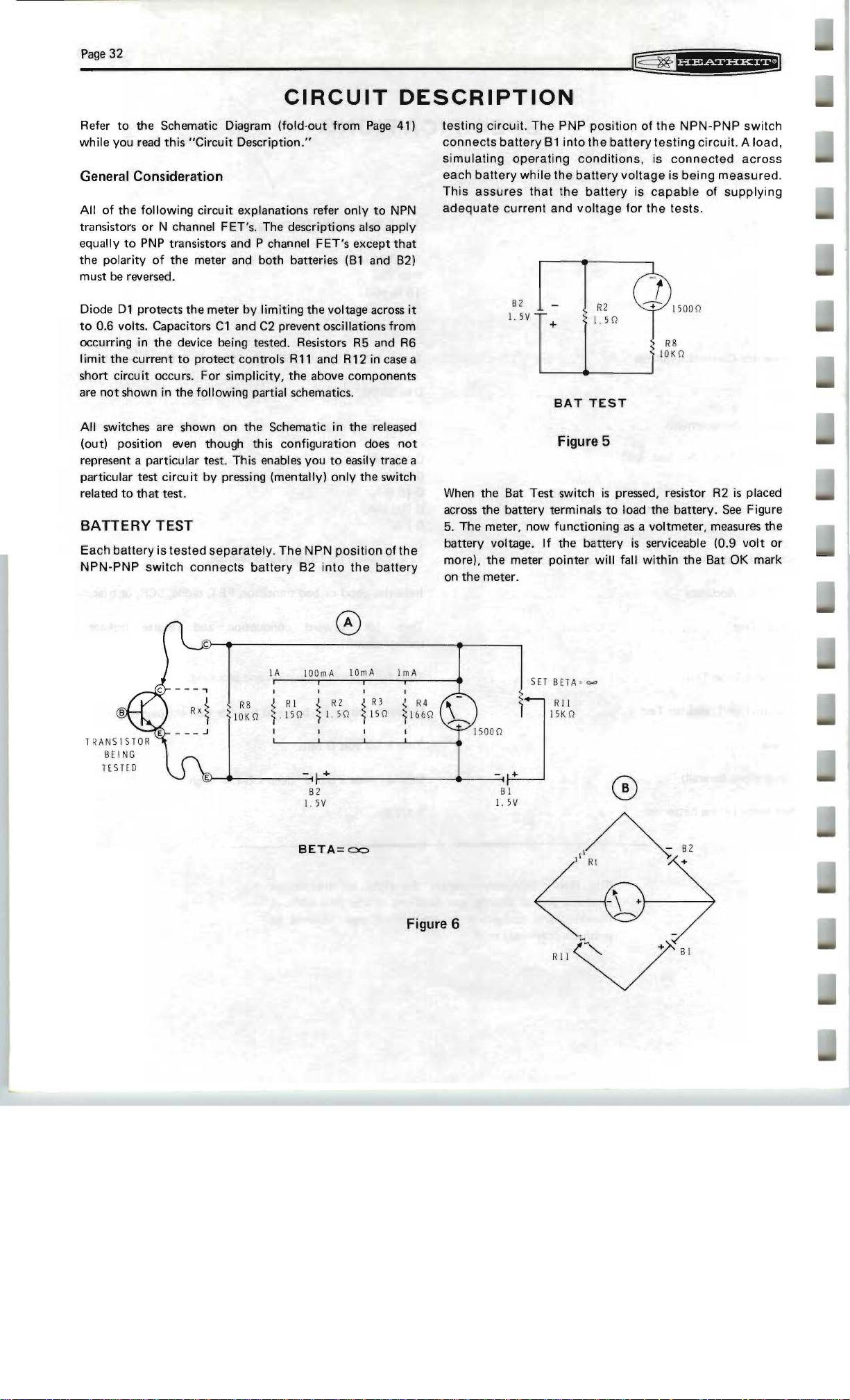
Page
32
I~~
fUMf*!{*iil
Refer
to
the Schematic Diagram
while
you read
this
"Circuit
General Consideration
All
of
the
following
transistors
equally
the
must
Diode
to
0.6 volts. Capacitors
occurring in
limit
short
are
All
(out)
represent a
particular test
related
BATTERY
Each
NPN-PNP
or
to
PNP
polarity
be
the
110t
switches are shown on
of
reversed.
D11protects
the
current
circuit
occurs.
shown in
position
particular
to
that
TEST
battery
switch
circuit
IN
channel F ET's. The descriptions ali
transistors and P channel
the
meter and
the
meter
device being tested. Resistors R5 and
to
protect
For
the
following
even
though
test. This enables
circuit
by
test.
is
tested
separately.
connects
CIRCUIT
(fold-out
Description."
explanations refer
both
batteries
by
limiting
C1
and
C2
controls R11
simplicity,
partial schematics.
the
th
pressing (mentally)
battery
the voltage across
prevent oscillations
the
Schematic in the released
is
configuration
you
The
NPN
82
DESCRIPTIION
from
Page
41)
only
to
NPN
so
apply
FET's
except
that
(B
1 and B2)
it
from
R6
and R 12 in
above components
to
only
position
into
case
does
not
easily trace a
the
switch
of
the
the
battery
a
testing
connects
simulating
each
This
adequate
When
across
5.
battery
more),
on
battery
assures
The
the
circuit.
the
the
meter,
the
meter.
The
battery
operating
while
that
current
62
1.
Sv
81
the
and
1+
I
BAT
Bat Test switch
battery
voltage.
now
meter
terminals
functioning
If
pointer
I
PNP
position
into
the
conditions,
battery
the
battery
voltage
R2
1.SI)
TEST
Figure 5
is
the
battery
will
of
the
'battery
to
testing
is
connected
voltage
for
pressed, resistor
load
as a voltmeter,
fall
is
is
capable
the
tests.
the
battery.
is
serviceable (0.9
within
NPN-PN
being
the
IP
circuit. A load,
measured.
of
supplying
R2
is
See
measures
Bat
OK
switch
across
placed
Figure
the
volt
or
mark
TESTED
~
RX~
R8
., 10K Q
1 A
i
)
0
100 m A
R 1
15Q
1
BETA==
10mA
~
R 2
I)
1 5
"1
+ -
82
5V
~
~
RJ
lS
l
I)
rn
A
~
~
166
Figure 6
R 4
SET8 ETA·c,a
R
11
IS K
I)
+
B 1
1. 5v
I)
®
//~
I R l
82

Page
33
BETA =
The
primarily
resistance, R8,
This
Figure 6.
in-circuit
circuit
means
of
in
transistor
Resistors R 1
1 A
does
00
"beta
=
compensates
circuit
Resistor
resistance,
to
another,
of
balancing
beta
can
now
subsequent
collector
through 1 mA
not
use a
00"
circuit,
and
is
basically a
be
tests
through
meter
as
shown
for
in-circuit
Rt
Rx . Because Ax varies
control
the
achieved
current.
ranges
shunt
resistances,
bridge
represents
R11 (Set
bridge
since
will be
R4
are
meter
respectively. The
resi
the
circuit
load
circuit
any
directly
stor.
in
transistor
. A
shunt
Part A of
Rx.
as
shown
resistor R8 plus
Beta
true
unbalance
associated
resistances
Figure 6,
collector
in
Part B of
widely
from
= 00)
provides
representation
that
with
100
flA
load
any
one
occurs
the
for
the
range
BETA CAL
The
base
through
7.
Control
until
sufficient
place
the
collector
you
selected.
a
Because
resistance,
the
following
the
collector
Notice
This
total
than
the
range. Thus, when
read
will
of
the
transistor
control
current
that a shunt
resi
R12
R12
adjusts
collector current
pointer
is
resistor
the
meter
tests
cu
rrent.
resistance
stance
1/
10
the
(Beta Cal)
over
now
R 1 0
and
to
measure
resistor
(R
of
the
the
meter
current
is
now
and
the
base
the
CAL
equal
to
is
the
same
resistor A10
base
is in parallel
1 0
and
its
meter
is
placed
measured
connected
resistor
current
flows
through
X10
mark
the
particular
value as
can
current
shunt)
and
its
in
in
into
R10.
of
(full scale) .
be
interchanged
without
with
is
ten
shunt
the
the
collector
the
See
the
transistor
the
current
the
resistor
times
for
base
circuit,
circuit
Figure
meter
to
The
range
meter
in
changing
R10
larger
the
same
circuit.
.
it
"
""
STOR
B
l
l
~
T£
~
~l:
(B
* RI2
r
25
RIO
1500
1)
..
RIJ
\,000
IF
C
OUT
'"
l'
0KIl
0.
O~T
ROL
IIA
RA
n "
)
'-../
___
~
~
R 8
1
.4
~
f
~f--+--------<t--!--------+-----<'f-±---
100
r)
A I
01'1
I)
A
I
I
R4
1
col'
~
BETA
IA
,
~
R 2
) 1
.5
0
1
IS p u
GE 0 LYI.
ll
~
)
1;
ED
R 3
! LlOr A I
R I R2
~
I 5
r.
l.
'1
62
I.
JV
I ,
')
A
] OPl
CAL
Figure 7
OnA
ImA
I
I
I
,
,
5
()
~
R
,
~
166
~
I)
+
I 500
RJ
f
151)
()
1.5
B I
SET
BE TA,
C>Q
~
4-
Rl i
I
V

Page
34
,
R x S
~
~
----------
~
I
Om
~
"
)
A
fil
A
I
I
I
R4
R3
'>
) 1
50
660
1
RI O R
'>
1
5000
"
+
B 1
1. 5V
SET BEl A
'>
I
11
I A
10
0mA
I
J
~
)
I S
R1
~
R 2
)
150
'I
--~~+-------------------.------~
B 2
I. SV
BETA
This
circuit
meter
is
now
collector
resistor
meter, only
deflection_
Since
current
computed
into
in
For
the
over
10
the
meter
beta
10. The
circuit. See Figure 8. Also,
that
beta,
(fb),
account
terms
of
example, when
Beta
Cal
the
CAL
mA
flows
base
pointer
of 1 times
same
is
similar
to
the
beta
in
the
base
circuit
was previously across R
1/10
the
current
by
definition,
these
to
obtain
the
currents
currents
beta
. However,
and
could
beta.
the
10
mA
control
through
circuit,
result can be
is
Xl0
mark
the
assume
will
deflect
a multiplier
adjusted
(full scale), a
device . Now,
that
full scale
of
obtained
cal
dnd resistor
is
required
is
collector
be
their
current
to
almA
10
(CAL
IA
I
~
R2
) I . 5V
circuit
because
lOis
for
current
measured
the
meter
ratio,
and
range
place
the
collector
when
current
(1
mAl
Xl0).
from
the
100m A
I
~
R3
)
1
5V
except
Rl0
the
now
across
full-scale
and
scale
reads
is
selected, and
meter
current
the
meter
flows.
and
indicate
Thus
formula
10 n1 A
~
R 4
)
1660
Figure 8
that
the
is
in
the
shunt
the
meter
(Ic)/
base
the
ratio
takes
directly
pointer
is
The
,
beta
:
1
mA
BETA
IC = 10mA=
IB
1 mA
lebo, lees, AND leeo
Leakage
meter
transistor
to 1 ampere, depending
the
microamperes
the
lebo
the
open
lees
of
the
in
connected
a
Ieeo
=
the
open
currents
(and
leakage
circu it.
is
the
collector
(unconnected)
is
the
collector
is
the
collector
(unconnected)
10
are
its
shunt
leads.
The
currents
(pA),
measurement
and
the
. See Figure 9 .
measurement
and
the
to
the
emitter
measurement
and
the
. See Figure
measured
resistance)
meter
indicates
on
the
are
quite
the
transistor
of
the
base
of
of
the
emitter
. See Figure
of
the
emitter
by placing a
in
series
leakage
current
small, usually
must
cu
rrent
the
transistor
current
of
the
transistor
10.
current
of
the
transistor
11.
with
range
be
that
that
that
battery
two
current
selected
measured
removed
flows
with
the
flows
with
flows
with
and
the
of
the
from
. Since
from
between
emitter
between
the
base
between
the
base
0
in

~ ~fff:iSSiif{*iiU
________~__
________________________________________________________________
P_a~g~e_3_5_
IA
I
R 1
.1
50
~
lA
~
R I
~
.
150
100m A
R2
1.5 0
~
100m A
I
{
R2
)
I.
10m
50
A l
Rl
150
~
lebo
lam
A I
S
R3
~
1
50
lees
mA
R4
1
660
~
Figure 9
mA
~
R4
~
1660
B2
1.5
1
50
0 0
...
V
NS
I ST
BE I N G
TESTE
I STOR
BE
l NG
TE STED
OR
D
TRA
15
00
0
T
RANS
I A 100mA l amA
I R I
~
S
. 1
50 ~ 1.50 ) 150
R2
~
R3
Lceo
l
mA
I
~
) 16
R4
Figure 10
60
Figure
u v
11
1500 0
T
RA
BE
TE
NS I S10R
l G
STED

Page
36
~---------------------------------
11§j-:
ff'=MiUHfi
fE r
L-
__
Gm=O
Figure 12
Figure
SET GOI
,
R II
,--~-
~
1
5k
0.
HI
I.
SV
B I
l.
SV
Gm
13
0
R II
IS k
0.
Gm = 0
Battery
series with
Figure 12. This
will be used
Gm test.
pointer
not
may be
B1
and
the
Control R11
over
connected
connected
to
the
Gm
control
meter
circuit
measure
R11 (Set Gm = 0) are placed in
and
shunt
resistor
forms a
the
is
shunt
source-to-drain resistance in
adjusted
here
0 mark (full scale). Notice
into
the
circuit
at
this time, even
to
the
Tester
.
L..
type
to
_______
R7
as
shown
ohmmeter
place
the
that
the
though
GATE
that
meter
FET
SET
Gm' O
B2
+
l.
sV
70.
1 I
-T
GATE
14
Figure
typical
2
13
. Notice
ohmmeter
that
scale.
./r/~
RY
4 .
Figure
in
the
this test,
connected
in
the
shunt
drain
In
drain-to-source resistance has a Gm
is
is
it
because
drain-to-source resistance
is
because
the
the
FET
FET
shunts
the
and
with
shunts
Gm
meter
source
the
meter.
most
of
is
high,
the
very little
scale
leads
An F ET
that
the
meter
Gm
meter
is
similar
of
the
with
approaches
current.
approaches
current.
FET
00.
O.
to
are
a low
This
If
the
This
a
Because
resistance,
Gm
(transconductance)
an
ohmmeter
type
is
the
circuit
can measure Gm . See
reciprocal
of
Typically, values
,umhos
(the
meter
of
transconductance
indication
multiplied
by
are
1000).
expressed
in

~
"
fU=,'rififHii
_____________________________________
OO
IA
{ In
f . 1 5
mA 10 m A I
I
\1
Z R3
~
15\1
lil
A
I
~
) 16 6
R4
1 50 0
\1
82
I.
5 V
\l
P_a_g_e_37
I A 100m A
,
. 15
R I
Z R 2
II
11.
~
~
5\1
ID OlA
I I
I R
~
15
\g55
\l
[d55
Figure 15
i
R4
) 16 6
\1
Figure
B2
1.
16
5 V
1
50011
5
rET
8l l,'>I
TE
F
ET
BE
I [\G
TES TED
G
STED
GATE
The
14. However,
of
the FET
1 AND
"Gate
the FET
1"
the
GATE
circuit
Gate 1 test
2
is
similar
places a reverse bias
through resistor R9. Th
to
become
electrically narrower, increasing its
to
the
Gm circuit. See Figure
is
causes
the
on
channel
resistance, decreasing its Gm. A noticeable decrease
should be
If
apparent
the FET
reverse bias
should also be
Igss
AND
Idss
Leakage currents are measured
meter (and ,its
when
the
Gate
1 switch
is
a dual gate device,
the
second gate. A noticeable decrease
apparent
shunt
when
resistance)
the
the
Gate 2 switch
by
placing a
in
series
Gate 2 switch will
with
is
pressed.
battery
is
two
the
gate
of
in
Gm
in
Gm
pressed .
and
the
of
the
FET
leads. The
meter
ampere, depending
leakage
microamperes
currents
(riA),
circuit.
19ss
is
the
measurement
the
to
the
1dss
the
dra in and
to
the
gate and
is
the
source
source. See Figure 15.
the
measurement
the
source.
See
indicates leakage
on
the
cu
are
quite
the
FET
of
of
the FET
of
source
of
the
Figure 16.
current
rrent
range selected. Since
from 0
small, usually measured
must
be removed from
the
current
the
current
FET with
with
that
flows
the
drain
that
flows between
the
gate
connected
connected
to
1
the
in
the
between

Page
38
B1---.::
~
CHASSIS
PHOTOGRAPH
/
I
S13 S12

~
.f¥:,!1S;hi!j
Page
39
NOT E :
you
foll owi
can
L
To
ng
identify a
order
ways :
A.
B.
part shown
a replac e
Refer
installed
and no te the "Descrip t
(for exa mple: 1
Lo
ok
List."
CIRCUIT
in
ment, pro
to
up this Descript
one
ceed
the place where
in
the
Step-by·Step instructions
500 nor .005
BOARD
of
these Views, so
in
either
the
ion"
of
the
flF).
ion in
the
of
part
" Parts
the
is
part
X-RAY
2.
10
"
12
VIEWS
Note the ide
A.
(R-nu
Locate the same identification
B.
(next
"Description"
near
C.
Look up
Lis
11
10
12 3 12
13
14 5
15
18 7 16 7
17
D~M
~
ntification
mber
, C-number, etc.).
to
the
part)
the
part
.
th
is Description
t."
'0
2
11
'I
1
13
14 5
61
1'5
8
17
18
Q)~
of
on
the
4
8
number
the
Schematic.
part
will also appear
in
-c:::EJ-
-GO-
of
the
part
number
The
the
"Parts
4
5
~
~~
~
i;
~
~.
6)(})
CG)
-aD-
(VIEWED FROM COMPONENT SIDE)
0
~18
J
~
10
11
12 3
13
1.
15
16
7
r
~
81
U
~
8 5
1 3
10
11
12
10
11
12
_
•
G6
----
~
~
""
'
'-71,
~8
01
3 1
'---,
,,,
'"''
'".,
:'
" "
"
' "
"
p -
,- "'"---or
' 511
L
____
"
':
"
,
--
I'
IL' ________
J
:::::
:'"
,";'
,,:
':,,'
,
rM\
~
""
,~
9j
!\
"""
,
':
,, ,
'
II 59
510 "
~
§
r.
'18
9,
:;:~:
i
:"
,: I
-=;:--'"
r--
''''
, " " :' ,:
'''',
,,,
:"':
,
" " " " " , " , , ,
" " "
" " 0 "
' . , , , =
,
, ,
'l
--,.
II oI
" " "
J!.
____
_
~
[§
~
'
-
~
i , "
__
LI,
"
____
_
=';~b;~~~-J--,
~
...."__
...
'"
(VIEWED FROM FOIL SIDE)
, " "
r..,"",~
CE?
~~'&~
~
~
,
~
-J
,
,,,,'
~
:':::
':
::
L--'-,.L-,r"
;-,'
,
____
, _
~=--
01::
, , "
__
'"''
:T
"
'''',
I:::,
:,,;1
''''
"
,,,"
, J
56
."
,IL
_J~
--
--=------
G-
__
,
,--,
'"''
,,,.,
'".
1:
:'
~--..J-r---'I
____
'"''
,,,:,
: ";" ":17 "
::
:,8
, , , "
: ~ :
:'
,,-_.,----
'
__
r-,
~:,
::
::
: ' " L--,
L_1.•__
"
:,
__
r "
::
:.
:,
JL
____
,
':
1:
,
:
,

Page
40
--------RANGE
9 9 9 9 19
"
.'
~
~
, I I I
'm
II! I
~ ~
!
I I I I
1 I I I
I 1 I I
I I I I
I I I ,
I I , I
I I I I
I I , I
1 I I I
l
I I I I
I I I I
I 1 1 I I
L
_______ l ______ l _______ L______
S 16
1
1
BARE
I? i
1
I
',
'11
,
SA
" HI ,
5
vIOL
H D
6
7
8 BRN
BI K ,
9
B AR
10
I I
11
13
"
15
16
17
I!
" .
'!
""
1
or.
~ ~ ~
15
S
BAR
E
,
11
HI
W
HI
q[
i A
SA
RE l
\
'J
~ll
BARE
:
\'I
HI
l.
--
IBL"'''''
'S
I
.1 :
J
S 14
S!
al
K &
BARE
V,
HT
RE
,
BA
Rf
CR~,
I'IHI
I
I,
WHi
WH
l
G
~AY
-
'-
PUSHBUTTON
NPN/
PNP
S 11
J
.
SWITCH
-MODE
WIRING
1--
-----
FUNCTION
------
....
Q Q Q o lQ Q Q Q Q Q
~'
5
10
-.lHT
WH!
HT,
YEl
RED
REO
j
Hl
11(-
5lK
~
•
1.
______
Sq
-
,
, ' m
I I I I I I
, I I I I I
I I I , I I
, I I I I I
I I I I I I 1 I I
\.
______
II
S
W
~l
'
GRAY
's'
VIOL
IV
Y El
I'IH r
BR~
l:iHT
8lK
B R' ,
\l
ORC
\";
WI~
C~'I
J
-i--;-
'
56
WHI
I'/H
.. t ·
iLK
WHT
\"i-tT
,
, ' m
..
______
.L
______
..1
__ _ ____
, l
54
55
\"H !
1
/10l
,
n Hl
\'
J}oi
l
VEL
"HI
WHl
Vl
HT
CP
"
\'
/H
I ·
ORG
-
GP
\'."".
CRA,
BRh
\
N
HI
W
l-l
·
'/101
"
~-
,
I 1
.•
-l
,
, , ,
, , ,
,
, ,
, , ,
, , ,
, , ,
,
,
,
,
, , ,
, , ,
, , ,
, , ,
..&
I a S 7
Wri
T
IVHI
RE
0
W/il
\'trff
dill
VlH!'
WHT
Bl K
\;
h" \.'
GR"
..
______
51
"H
RLD
~
'"
" :
I
,
, ,,
, ,
.'
.)
, ,
,
, ,,
, ,
.L
______
I I
IK-rA
~
m
It
I
I
J
I
I
I
"
,
I ~ 1
,
r
Cl
OJ.

Page
41
G2
G,
B E
s
o
c
- -
--
S ••
Q
,
I
L
_______ I ______
-RANGE
1
00m
A
10mA
lmA
515
514
5 13 512
o
o
!l
2
"
!'rP!
I I I I
@ I 3
!
, I I ,
1 I I I
I , , I
1 I , ,
, I , I
• I I •
, I I ,
I I , I
• I I I
I , I I
I I I I
I I I I
I I I I
L
!l
C)
L..0
1 )
o
~
"
"I
I ,
L_______
100,UA
0
"2
I
BLANK
8'
J
L______ J
NPN/ PNP
N C
HAN
/
P
CHA
N
SI1
Q
,
~
I
MODE
rtT
TRANS
5'0
Q
Q
,
91l["P)
,
~~l,h)
, ,
: 0 6 I
'
l:ifV
'~
1
:,lli>
,
1 0
,
',
..n
'
Lk
.
' ®
· ,
.
· ,
.
.
·
.
\
. .
\.
______ L______
VIEwED fROM TOP
or
SWITCHES
-
,
BAT.
TEST ON/o
58
o
e:
..
:;
'
i
,
.
I
,
:
,
.
,
.
~
,
,
,
~
57
Q
~
:
'
::
:s
_,,, 0 J
rr
ICEO rCE S
lOSS
S6
Q
,
,
l
I , I I I
~------~---
FUNCTION
ICBO
GATE
Q
,
2
BETA BETA
GATE
Q
,
1 COm G m=O
IG
SS
Q
,
\ "
I "
I "
. "
___~_______ L ______
- -
5:1
Q
CAL
•
·
·
•
,
·
•
·
,
·
,
,
,
,
,
,
,
--
~
______
BETA
o
, ,
o
!
- -
:::CX)
S'
.
~
,
,
,
•
.
,
•
,
,
,
,
,
,
,
,
,
.
~
'
1
I
'V
)¢O~ ~··r.
..?h~'::#
~
r,o
rn
4 U.
QU
Ht r A:I!'.I OYl 1·.
:5,"''''C''
[
III
~U'.jUIt~
A
..
" T
",>
..
~
r
.-,
ND
SCHEMATIC OF THE
HEATHKIT"
FET/TRANSISTOR TESTER
MODEL IT-3120
US
I
'j.TDIo'!t
",iH
II,
'
N~TT
j,"
C
CUII
AP
'J;
I., C ITO~
"~T
......
DIr.
...
"~oJ
ln'j~D
IOAR'D
(aPH~O\S
tQUBPO'~ D
YH h
"i
lUU
T£ ~ cl "o~·qS[
~H
'PO ,',\
'tf(
10
THO~t S~OWN
Hi u'
';N
TH[
UM :
'\IO T"nO'
!J ! [l'IjO
C
IIII(U
SS.
DI H£iillflIH
Q/i!
Ii
O
,
(If"
~ S
lIO,' PD
r;
THt !l.CH(lM
iP
ICI'
COo\ll(IHH
SHOWl\.
fO
COPlUOl LUG
nC
I[
lI
OR
It
~
~
~n
"
;~
IHiP
x -
R'"
.AU
('olEN
C;OM
II
D
'H'~
[;0
ro
,,,,( CHAS'$,I\
YI
[ W
rOil! I Hl
S,"IIC~(S
APE
IHOUGH
IHI'
IGJ
UIIOtl
H"
'I
Ot l '.CI[
1
•
"
'!(II!)II
~1
PHoroe",
PH't'S
~HO""' "
00
'01
A!l
2 1
,,,
IC
" L LOt
I~
THE
rtrPAlSENT "
!)
A
UHU[D
3
PH
ANa
[lilr;
Ul!
..
t IDtJ 01
P"'US
IHL[AHO IDUll
SPECifi
(11i'C.UI!
ICI
POS
C
opr ~
aOAii D
,I,
lHl
'110
"'I~n
'l
j
 Loading...