

Page 1

HEATHKIT
®
MANUAL
5 Megahertz
Dual Trace
Oscilloscope
Model 10-4205
595-2072
.·':::;_·. 7 ...
·.
'·
.
. ·
..
, ,,_
~:···
...:::
.....
.
;~~:.
·.:
.. · .:
..
·
::·.:.~--~
0
L~~-;·-~
HEATH
COMPANY • BENTON
HARBOR,
MICHIGAN
Page 2

HEATH COMPANY PHONE DIRECTORY
The following telephone numbers are direct lines to the departments listed:
Kit orders and delivery information
Credit
......... .
Replacement Parts .
......
....
.....
. . . . .
.................. .... (616) 982-3411
................
.....
. . .
..................
Technical Assistance Phone Numbers
8:
00A.M.
RtC, Audio, and Electronic Organs ..
Amateur Radio
to
12
.....
P.M.
...
and
...
1:00 P.
M.
....
...............
to
..
4:30P
. .
......
Test Equipment, Weather Instruments and
.......
. . .
.......
. .
...
Home Clocks . .
Television
............... ....
....
...
......
. . . . . .
............
Aircraft, Marine, Security, Scanners, Automotive,
Appliances and General Products
Computers
..
. ....
....
...
. . .... . . . .
..........
......... ....
......
...
. (616) 982-3561
(616) 982-3571
.M., EST, Weekdays Only
...
......
(616) 982-3310
...
. . . . . . (616) 982-3296
. .... .... (616) 982-3315
(616) 982-3307
......
•...
. (616) 982-3496
...... (616) 982-3309
YOUR HEATHKIT 90 DAY LIMITED WARRANTY
If
you are
not
satisfied
with
our
Services, Heath Company, Benton Harbor,
attention.
Our
attorney,
who
happens
phrases in order to
For a period of ninety (90) days after
either in materials or workmanship. You
telephoning
warrant
We
and
used in accordance with
If
a defective part or error in
fault of yours, we will service it free
Electronic Center (units of Schlumberger
You will receive free
drop us a
Our
incorrect assembly, misuse, fire, or by
advertised.
This warranty covers only Heathkit products
our
limitation of incidental or consequential damages , so
gives you specific legal rights,
line
warranty does
products. We
comply
us at (616) 982-3571.
that
during
consultation
or give us a call. Sorry,
not
Our
warranty does
are
service- warranty or
to
be
with
the first
ninety
our
design
cover
and
not
not
responsible
and
quite
a kitbuilder himself, insists that
the
new
purchase
can
And
we'll
(90) days after
printed
has caused
upon
on
any
problem you
we
we
are
not
unauthorized
include
for
you may also have
otherwise-
Michigan
warranty regulations. Fine. Here they
, Heath
obtain parts directly from Heath
pay
shipping
instructions, will meet published specifications.
your
proof of
purchase
Products
cannot
accept
responsible for
reimbursement
and
is not
incidental
HEATH COMPANY ~
BENTON HARBOR, MI. 49022
oROOo&~uoOOOootooooomo~
or
with
our
49022. He will make certain your problems receive
Company
purchase,
Heathkit
Corporation). or
will replace or repair free of charge any parts that are defective
charges to get those parts to
our
product
and
might
encounter
collect calls.
damage
modifications to or uses of
for
customer
extended
or
consequential
the
above limitation or exclusion may not
other
rights
products, write directly to
we
describe
our
warranty using all the necessary legal
are
:
Company
products,
to
malfunction
delivery at your expense to the Heath factory,
any
of
our
in
the
caused by
assembly or set-up time.
to allied
equipment
damages.
which
vary from state to state.
by writing us at
you-
when
correctly assembled, calibrated , adjusted
during
authorized
assembly or
the
use of corrosive solder, defective tools,
our
products for
or
components
Some
states
our
anywhere
the
warranty period
overseas distributors.
use
of your Heathkit product. Just
used in
do
not
apply
Director of Customer
immediate,
the
address
purposes
allow
to you. This warranty
personal
below or by
in
the world.
through
any
Heathkit
other
than
conjunction
the
exclusion or
no
as
~
with
~
~
~
Prices and specifications subject to change without notice.
Page 3

Heathkit® Manual
for
the
5 Megahertz
Dual Trace
Oscilloscope
Model 10-4205
595-2072
HEATH
BENTON
COMPANY
HARBOR,
MICHIGAN
490
2 2
Copyright © 1978
Heath Company
All Rights Reserved
Printed in the United States of America
Page 4

Page 2
TABLE OF CONTENTS
INTRODUCTION o 0 0 0 0 0 0 0 0 0 0 0 0 0 o o o o 0 0 0 0 0 0 0 0 0 0 0 0 3
UNPACKING
ASSEMBLY NOTES
o o o o 0 0 0 0 0 0 0 0 0 0 0 0 0 o o 0 0 0 0 0 0 0 0 0 0 0 0 0 0 4
0 o o o o o 0 0 0 0 0 0 0 0 o o o o 0 0 0 0 0 0 0 0 0 5
VERTICAL CIRCUIT BOARD
Parts List
Step-by-Step Assembly
0 0 0 0 0 0 0 0 0 0 0 0 0 0 0 0 0 0 0 0 0 0 0 0 0 0 0 0 0 0 0 0 0 8
0 0 0 0 0 0 0 0 0 0 0 0 0 0 0 0 0 0 0 11
HORIZONTAL CIRCUIT BOARD
Parts List
Step-by-Step Assembly
0 0 0 0 0 0 0 0 0 0 0 0 0 0 0 0 0 0 0 0 0 0 0 0 0 0 0 0 0 0 0 0 33
0 0 0 0 0 0 0 0 0 0 0 0 0 0 0 0 0 0 0 36
POWER SUPPLY CIRCUIT BOARD
Parts List
Step-by-
0 0 0 0 0 0 0 0 0 0 0 0 0 0 0 0 0 0 0 0 0 0 0 0 0 0 0 0 0 0 0 0 50
Step
Assembly 0 0 0 0 0 0 0 0 0 0 0 0 0 0 0 0 0 0 0 52
CHASSIS
Parts List
Step-by-Step Assembly
INITIAL TESTS
CALIBRATION
0 0 0 0 0 0 0 0 0 0 0 0 0 0 0 0 0 0 0 0 0 0 0 0 0 0 0 0 0 0 0 0 59
0 0 0 0 0 0 0 0 0 0 0 0 0 0 0 0 0 0 0 61
0 0 0 0 0 0 0 0 o 0 o o o 0 0 0 0 0 0 0 0 o o o o o o o 0 o 80
0 0 0 0 0 0 0 0 0 0 o o o 0 0 o 0 0 0 0 0 0 o o o o 0 0 0 0 82
FINAL ASSEMBLY
OPERATION
IN
CASE OF DIFFICULTY 0 0 0 0 0 0 0 0 0 0 o o 0 0 0 0 0 0 0 o
o o 0 0 0 0 0 0 0 o o 0 0 o 0 0 0 0 0 o o o 0 0 0 0 88
0 0 0 0 0 0 0 0 0 o 0 0 0 0 0 0 0 0 o 0 0 o o o 0 0 0 0 0 0 o 0 89
97
SPECIFICATIONS 0 0 0 0 0 o o o 0 0 0 0 0 0 0 0 0 0 o o 0 0 0 0 0 0 106
THEORY OF OPERATION
CIRCUIT DESCRIPTION
0 o 0 o o o 0 o 0 o 0 0 0 0 0 o o 0 0 108
o o o 0 0 0 0 0 0 0 0 0 0 o 0 0 0 0 0 0 0 109
SEMICONDUCTOR IDENTIFICATION
CHART
0 0 o o o o o o o 0 0 0 0 0 0 0 0 0 0 0 0 0 0 0 0 0 o 0 o 0 0 0 0 0 0 116
CIRCUIT BOARD X-RAY
VIEWS
0 0 0 0 0 0 0 0 0 0 0 0 0 Illustration Booklet, Page
36
SCHEMATIC DIAGRAM 0 0 0 0 0 0 0 0 0 0 0 o 0 0 0 0 (Fold-in)
WARRANTY
0 0 0 0 0 0 0 0 0 0 0 0 0 0 0 0 0 0
CUSTOMER SERVICE
0 0 0 0 0 0 0 0 0 0
Inside
Inside
front cover
rear cover
Page 5

;
;
:
INTRODUCTION
The
Heathkit
cilloscope is a compact, versatile, easy-to-build, electronic
waveforms
to
measure
to 5 MHz
ity of
the
Oscilloscope for nearly all
tions. The
many
and
other
capabilities
priced
Model
instrument
in
10-4205, 5 MHz, Dual-Trace Os-
that
electronic circuits. You
frequency,
bandwidth
and
vertical amplifiers
triggered
horizontal
outstanding
that
are
oscilloscopes.
you
and
the
types
features
usually
can
AC or
excellent
allow
of waveform
sweep
found
use
DC
voltages.
provide
to
can
input
you
circuit
only
study
also
use
The
sensitiv-
to
use
applica-
and
accuracy
in
higher
the
DC
this
the
it
easier
to
trigger
on
the
vertical frequency of
a TV set.
• A
10
to 1 attenuation
for signals
input
tal
applied
jack.
circuit
to
that
the
external, horizon-
• Accurately calibrated vertical
with
variable controls.
• A calibrated
selections, variable
time
base (seven
within
each selection).
Page 3
can
be
used
attenuators
time
base
Among
fers are:
• A
the
many
special
This
rejecting
other
TV
allows
high
features
position
low
frequencies
frequencies,
this
Oscilloscope of-
on
the
trigger selector.
to
thus
pass
making
while
it
These
make
features, along
this
Oscilloscope a
with
laboratory, service shop, or
the
attractive styling,
welcome
the
ham
shack
asset to
.
will
the
Page 6

Page 4
UNPACKING
Inside
which
box removed from
bags
will refer to these areas as
rected
All other parts
ered
parts from
specifically called for
the
shipping
contained
stamped
to
open
the
"final
their
carton
this
the
PACK 2
each
of
in
the
pack."
bags or
Assembly Manual.
shipping
through
these
shipping
Caution: Do
the
in
was
the
box
carton, you
PACK 4.
"packs."
"packs"
carton
"final
pack"
a Parts List
stamped
The
You
as
it
will
not
until
in
the
With
will
Manual
will
be
is needed.
be
consid-
remove
they
Manual.
PKl
this
find
di-
any
are
Each assembly section of
"Parts List"
At
tions.
be
instructed
be
directed,
parts from
and
the
beginning
to
in
the
"Step-by-Step Assembly" instruc-
open
one
some Parts Lists,
final pack.
the
of
Manual
each
of
the
contains its
"Parts
List," you
packs. You
to
remove
will
certain
own
will
also
Page 7

~~~~;allllll;ll:ll=u~
.................................................................... ..
ASSEMBLY NOTES
TOOLS
You
will
need
these tools to assemble
your
kit
.
Page 5
PLIER S
-------------------------------------------------
OTHER
HELPFU~
TOOLS
/
NUT STAR
1IMAY
I WITH" KI TI
I
I
I * TO
BE
SUP
TER
PLIED
DIA
GON
C
UTT
~
DE SOLDERING
AL
ERS
BUL
B*
ESO
LDER I NG
D
BR
AID
*
REMOVE SOLDER FROM
CIRC
UIT CON
NECTIONS
HEATH
KI T
SOLDERING
RO
N
I
OR
PENCIL
SO
LDERI
TO 40
NG I RON
WATT
S!
125
.
·------------------------------------------------~
ASSEMBLY
1.
2.
Follow
tire
The
rials
eration
generally
directed
following
until
another
the
instructions
step before
you
illustrations
and
Details. Pictorials
for a
group
illustrate a
to refer to a
steps,"
you
are referred
group
of steps.
perform
in
the
Manual
of
single
certain
continue
to
carefully. Read
each
operation
are called Picto-
show
the
assembly
step.
steps
When
Pictorial
using
that
another
Pictorial for
the
en-
.
overall op-
; Details
you
are
"for
the
Pictorial
3.
4.
5.
Most kits
that
etc.)
Keep
sembly
ranged
Position
use
contains
that
are too large for
the
"Illustration Booklet"
Manual.
in
Pictorial
all
Solder a part
are
instructed
a separate
"Illustration
Booklet"
illustrations (Pictorials , Details,
the
Assembly Manual.
with
the
The
parts
or a
to
illustrations
number
as
shown
group
of
do
so.
sequence.
parts
in
in
the
Pictorials.
only
it are ar-
when
As-
you
Page 8

Page 6
6. Each circuit
component
numbers
part
in
These
part
has
In
At
part
number
when
the
various sections of
numbers, which
to
be
the
Parts List,
the
beginning
component
In
some
In
the
Schematic,
In
the
section
7.
When
you
are
particular
vided
at
length,
the
bottom
SAFETY WARNING:
off excess
fly
toward
lead
your
lengths.
eyes.
in
an
electronic kit
(R2, C4, etc .
you
want
are especially
replaced
, appear:
of each step
is
installed,
illustrations,
at
the
instructed
use
Avoid
Hold
of
to
the
the
eye
the
has
its
).
Use
these
to
identify
the
the
same
Manual.
useful
where
rear of
cut
something
the
Manual.
scales (rulers) proManual
injury
leads
when
so
they
pages.
you
cannot
own
if a
to
cut
SOLDERING
Soldering
will perform
der
connection
tween
circuit
vent
properly.
a
It is easy to make a
follow a few
1.
a
2.
two
board
an
otherwise
Use
40-watt
3/16"
Keep
on a wet
the
process is called
tip
When
the
ned.
is one of
while
will form
parts, such
foil. A
simple
the
right
pencil
chisel or
the
soldering
sponge
tip
to give
and
enable
solder
tip,
the
the
most
important
assembling
an
electrical
as a
component
bad
solder
connection
operations
your
kit. A good sol-
connection
lead
could
you
be-
and
pre-
well-assembled kit from operating
good
solder
connection
if you
rules:
type
of
soldering
pyramid
or
the
tinning, and
you
tends
tip
needs
soldering
tip
iron
tip
cloth; then
entire
to
to
tip a wet
make
"ball"
to
be
iron. A
iron
with
works best.
clean.
Wipe
apply
it
will protect
good
connections
or does
cleaned
a
solder
look.
not
and
25
to
1/8"
or
it often
to
This
the
stick to
retin-
a
.
Page 9

Page 7
PARTS
Resistors
in
0 (ohms),
will
kO
be
types of resistors
body,
while
others
The colors of
the
steps, therefore
for
information
Color
Black
Brown 1
Red
Orange
Yellow
Green
Blue
Violet 7
Gray
White
the
Band 1
1st Digit
Digit
called
(kilohms), or
bands
out
will
have
will
be
identified
and
the
following color
by
their
resistance
MO
(megohms). Certain
the
value
by
the
value
will
only.
Band 2
2nd Digit
Color
0
2
3
4
5
6
8 Gray 8
9
Black
Brown
Red
Orange
Yellow
Green
Blue
Violet
White 9
value
printed
code
BANDS
Digit
0
1
2
3
4 Yellow
5
6
7 Violet
on
the
a color
be
code
given
.
in
is given
: 1 2 3 / /Tolerance
Multiplier
Band 3
3rd Digit
Color
Black
Brown
Red
Orange
Green
Blue
Gray
White
1/4-WATT
==
==fllm-===OR~
1/2-WATT
(if used)
Digit
0
1
2
3 Orange
4
5
6
7 Silver
8
9
OR
1-WATT
*Note
Wide
Space
Multiplier
Color
Black 1
Brown
Red 100
Yellow
Green
Blue
Gold
=======~--~=
2-WATT
Resistance
Tolerance
Multiplier
10
1,000
10,000
100,000
1,000,000
0.
01
0.1
Color
Silver
Gold
Brown
Tolerance
:!:
10%
:!:
5%
:!:
1%
Capacitors
value
will
in
JLF
(microfarads) or
be
called
out
by
pF
(picofarads)
ceramic, Mylar* , electrolytic , etc.
may
have
their
value
ner
:
First digit of
capacitor's value : 1
Second digit of
capacitor's value: 5
Multiplier: Multiply the
& second digits by
first
the proper value from the
Multiplier Chart.
To find the tolerance of
the capacitor, look up
this letter
columns.
*
DuPont
in
the Tolerance
Registered
printed
Trademark
in
____
their
Some
the
following
_,
capacitance
and
type:
capacitors
man-
FOR THE
NUMBER:
EXAMPLES:
151K
759 = 75
NOTE:
decimal
MULTIPLIER
0
1
2
3
4
5
8
9
=:=
15 X 10 = 150
X0.1
= 7.5
The
letter "R"
pF
pF
may
be
used
point: as in: 2R2 = 2.2 (pF or
TOLERANCE OF CAPACITOR
1
10 pF OR
LESS
±0.1
pF
±0.
25
pF
±0.5
pF
±1.0
pF
±2.0
pF
LETTER
MULTIPLY
BY:
10
100
1000
10,000
100,000
O.D1
0.1
at
B
c
D
F
G
H
J
K
M
times
JLF).
to
signify a
OVER
10 pF
:±
± 2°/o
±3
±5°/o
±
±
20%
1o/o
o/o
10%
Page 10

Page
8
VERTICAL
CIRCUIT
Remove
each
correspond
part
the
parts from
against
to
the
the
BOARD
the
pack
following list.
numbers
on
the
marked
The
#1.
key
numbers
Vertical Circuit
Board Parts Pictorial (Illustration Booklet, Pages
and
2).
Any
part
that
is
in
an
the
envelope
step. Do
parts are
KEY
HEATH
Part
No.
individual
part
number
after
not
accounted
No
. Comp. No.
on
it
should
you
identify
discard any
for.
QTY.
DESCRIPTION
be
it
until
packing
envelope
placed
it
is called for
materials
back
CIRCUIT
RESISTORS
All resistors
(fourth
NOTE: The
velope
pack
1/2-Watt
AI
A1
A1
A1
are
15q
5%
silver).
resistors
RES).
you
check
band
(stamped
before
(p-
6-279
6-100
6-220 4
(fourth
may
Open
the
\.S
2
3 2.7
20
band
gold)
be
packed
all
the
resistors
3L
\
Y;·
tV\-G
n (Red-Viol-Gold)
10
n (Brn-Bik-Bik)
22
n (Red-Red-Bik)
unless
designated 1 0%
in
more
resistor
against
envelopes
the
M~)
than
one
Parts List.
~
tcf-i
R179,
R182
R124A, R124B,
R131A, R131B,
R142A, R142B,
R145A, R145B,
R157A, R157B,
R158A, R158B,
R159A, R159B,
R164A, R164B,
R166, R168,
R174
R147A, R147B,
R148A, R148B
PARTS LIST
Some
Check
1
with
into
the
in
a
until
all
en-
in
this
~
I R \05~
R181,
, R175
KEY
No.
Resistors (Cont'd.)
A1
parts
aging number.
purposes
List."
To order a
PART NUMBER. Use
with
the
Parts"
separate "
HEATH
Part No. Comp. No.
6-330
A1
6-390 2
A1
6-470 2
A1
6-820 2
A1
6-101
A1
6-201
6-221
A1
6-271
A1
A1
6-331
A1
6-391
A1
6-471
A1
6-511
A1
6-751
are
only
kit
.
inside
Heath
If
marked
These
and
with
numbers
do
not
replacement
the
one
is
not
available, see "Replacement
the
rear cover.
Parts Price List."
QTY.
DESCRIPTION
33
{
n (Org-Org-Bik)
n (Org-Wht-Bik)
39
47
n (Yei-Vioi-Bik) R134A, R134B
82
n (Gry-Red-Bik) R144A, R144B
100
6
2
8
2
2
6
2
2
2
n (Brn-Bik-Brn) R161A,
200
n (Red-Bik-Brn)
220
n (Red-Red-Brn)
270
n (Red-Vioi-Brn)
330
n (Org-Org-Brn)
390
n (Org-Wht-Brn)
470
n (Yei-Vioi-Brn)
510
n (Grn-Brn-Brn)
750
n (Vioi-Grn-Brn)
a "
171-
are
used
appear
in
the "Manual
part, always
Parts
Order
For
prices, refer to
" or
"172-
for packaging
include
Form
furnished
CIRCUIT
R1A, R1B
R2A, R2B
::::ftj:()SA, R4059;
R106A, R106B
R151A, R151B
R162A, R162B,
R171,
R117A, R117B
R111A, R111B,
R113A, R113B,
R114A, R114B,
R183,
R108A, R108B
R116A, R116B
R135A, R135B,
R139A, R139B,
R153A, R153B
R136A, R136B
R115A, R115B
R163A, R163B
" pack-
Parts
the
the
,
,
R16·1B,
R172
R184
Page 11

®
~
f§1%f#fB+@
Page 9
KEY
HEATH QTY. DESCRIPTION
No
. Part No. Comp. No.
CIRCUIT
Resistors (Contd.)
A1
A1
A1
A1
A1
A1
A1
A1
A1
A1
A1
A1
6-102
6-122
6-182
6-272
6-332
6-912
6-103
6-153
6-223
6-913
6-104
6-914
20 1000
2
1200
2 1800
4
2700
4 3300
2
9100
10
kfi
4
2 15
kfi
kfi
22
2
91
kfi
2 100
2 910
n (8rn-81k-Red)
n (8rn-Red-Red)
n (8rn-Gry-Red)
n {Red-Viol-Red)
n (Org-Org-Red)
n (Wht-8rn-Red)
(8rn-81k-Org)
(8rn-Grn-Org)
(Red-Red-Org)
(Wht-8rn-Org)
kfi
(8rn-81k-Yel)
kfi
(Wht-8rn-Yel)
R104A, R1048;
R133A, R1338,
R141A, R1418,
R146A, R1468,
R149A, R1498,
R156A, R1568,
R165, R167,
R185, R186,
R187, R188,
R191
R155A, R1558
R137A, R1378
R118A, R1188,
R122A, R1228
R119A, R1198,
R121A, R1218
R103A, R1038
R109A, R1098,
R154A, R1548
R132A, R1328
R169
R102A, R1028
R107A, R0178
R101A, R1018
Other Resistors
'/t..j
A2
6-1801-
~
IZ.
A2
6-4320-11
1-19-1
A3
A4
5-11-2
AS
3-55-5
CAPACITORS
Ceramic
81
21-7 2
81
21-121 4
81
21-75 1
81
21-722
81
21-140 2
81
21-36
4
4
2
2
2
n (1.8
k)
~
watt
,
1800
1%
(8rn-Gry-81k-8rn)
432
n' 1 /8-watt, 1% R125A, R1258,
(Yei-Org-Red-81k)
n, 1-watt, 10%
220
{Red-Red-8rn)
15
kfi
, 2-watt, 10% R176
(8rn-Grn-Org)
2000
n
(2
k), 5-watt R177, R178
33 pF C117A, C1178
56
pF C112A, C1128,
100 pF
330 pF C105A, C1058
.
001
JLF
.002
JLF
R123A, R1238,
R127A, R1278
R126A, R1268
R173
C116A, C1168
C121
C128, C129
C108A, C1088
, R192
KEY HEATH
QTY. DESCRIPTION CIRCUIT
No. Part No. Comp.
Capacitors, Ceramic (Cont'd.)
81
21-141
81
21
81
21-47
81
21-31
81
21-199 2
-27
1
4
3 .
.0033
.005
01
.02
JLF
.1
JLF
JLF
JLF
JLF
C131
C107A, C1078,
C135, C136
C109A, C1098,
C122
C124
C114A, C1148
Electrolytic
82 25-115
83
25-117 4
25-160
B3
8
10
JLF
100
JLF
3
250
JLF
C111A, C1118,
C113A, C1138,
C123, C132,
C133, C134
C118A, C1188,
C119A, C1198
C125, C126,
C127
Trimmer
84
84
84
85
31-56
31-54
31-52
31-77
4 1.
5-
2 4-40
4 8-60
2 80-400
20 pF C101A, C1018,
C103A, C1038
pF
pF
pF
C102A, C1028
C104A, C1048,
C115A, C1158
C106A, C1068
Other Capacitors
86 27-28
2 .1
JLF
Mylar
C1, C2
DIODES
C1
C1
C1
56-56
56-67
56-89
~
\(o
4
1 N4149
VR10A
G0510
g~e~A. o~e+So
9Hl2A., 0192&,-
0103A, 01038,
0104A,
0105A,
0106A,
0108A,
0109A,
0111A,
0112A,
0107
0113, 0114,
0115, 0116
No.
01048
01058
01068
01088
01098
01118
01128
Page 12

Page
10
KEY HEATH
No. Part
No.
QTY.
DESCRIPTION
CIRCUIT
Comp.
TRANSISTORS-INTEGRATED CIRCUITS (IC's)
NOTE: Transistors and integrated circuits are marked for identification
in
one
1.
Part Number.
2.
Type number.
of
the following four ways:
(On
integrated circuits, this refers
only to the numbers and letters listed. Any additional letters or numbers
on
an
IC
are not signifi-
cant.)
and
3. Part number
4.
Part number with a type number other than the one
type number.
listed.
01 417-235
01 417-237
01 417-260
01 417-293
01 417-801
02
417-834
03
417-902
04
443-1
04
443-4
pi
LJll-
~Lf
8 2N4121 transistor
2 SE6020 transistor
4 2N4258A transistor
4 2N5770 transistor
4 MPSA20 transistor
2 MPSU10 transistor
4 5566 transistor
7400 IC
1 7472 IC
1../
"=>e1
eo
tfl.!M!?
I s
'\tJ
0106A, 01068
0107AI 01078
01
08A,
0109AI 01098
01131 0114
0104A, 01048
01
05A,
0111A, 01118
0112A
, 0 1
0103A
, 0 1
0117, 0118
0115,0116
0101A, 01018
0102A, 01028
U101
U102
f
DID\
1::>10\5
)
DIDZ.AJ
OTHER CIRCUIT COMPONENTS
E1
10-357
E2 10-917
E2
10-918
E2
10-936
E3
10-1118
E4
60-73
E5
60-624
E6
63-1316
E7
475-16
2 1 00
3 200
2
2
2
2
1
2
2
n control
n control
500 n control
1 000
ll
( 1 K) control
ll
( 1 K) control
1 000
DP3T 3-position slide switch
DP4T 4-position slide switch
Rotary switch with 5000
(5K) control
Ferrite bead
n
R112A, R112B
R152A, R152B ,
R189
R143A, R143B
R138A, R138B
R4A, R4B
SW1A, SW1B
SW3
SW2A-R3A,
SW2B-R3B
HARDWARE
#4
Hardware
No.
01088
01
05B
128
038
"))l
Z!S
KEY HEATH QTY. DESCRIPTION
No. Part
#6
G1
G2 250-33 4 6-32
G3 250-416 4 6-32
G4 250-56 4 6-32 x 1/4" screw
G5
G6 254-1
No.
Hardware
250-1282 3 6-32 x 1/8" black setscrew
x 1/8" setscrew
x 1/4" flat head screw
252-3 4 6-
32
nut
4
#6
lockwasher
Other Hardware
H1
253-50 2 1/4" plastic spacer
H2 252-7 4 3/8-32 nut
1
H3 255-145 2 3/8" spacer
1
1
MISCELLANEOUS
J1
,
,
,
,
75-769
J2 75-770
J3 266-1008
85-2043-1
J4
204-2315
204-2333
J5
206-1273
J6
J7
215-95
343-15
344-
346-1
347-55
390-1436
J8 432-892
J9 434-230
J10 434-298
J11
453-66
J12 455-44
J13 456-7
J14 462-1049
J15 462-1050
J16 462-1055
L 1 490-5
134-237
L2
260-16
L3 73-34
390-147
390-1255
390-1483
391-34
597-260
51
Slide switch cover (1-7/16")
Slide
switch cover (29/32")
Slide switch cover
Vertical circuit board
Sw
itch bracket
2 Control bracket
1 Circuit board shield
2 Heat sink
4' Shielded cable
3' Brn wire
8-1
/2" Sleeving
1-1
/2' a-conductor flat cable
1 Metal front panel
2 BNC connector
4 8-pin IC socket
2 14-pin IC socket
2 5" extension shaft
2 Split plast ic bushing
2 Shaft coupling
Red knob
2 Small black knob
Large black knob
Plastic nut starter
Cable with connector
1
2 Alligator clip
2 Red alligator clip insulator
Danger label
Fuse label
Power consumption label
Blue and white label
Parts Order Form
(1
-3/16")
CIRCUIT
No.
Comp.
J1
, J2
F1
250-428
F2 250-52
F3 250-186
F4 252-15
F5 254-9
0
Y.
}'2
I 1
(8
I
3~ 8
I"' I II II
Q .
I " ( 8 I 7
1 I I I
!5
1 (CM )
1 4-40 x 1/4" flat head screw
2 4-40 x 1/4" screw
#4
4
3 4-40 nut
3
"/.
~
8
I . I I I I I I
'2
x 3/8" screw
#4
lockwasher
(I
N C
3
HES
) 2
' I I
I'
"
3
,.
1, I I I I
e 7 · e
'I
I I I
' I
Solder
Assembly Manual (See Page 1
for Part Number)
'II
7
I
17
4
I I
I I I ' I
I
I ' I I ' I
11
10
9
5 6
·,I
I
12
I'
13
I l ' I I I
1 4
15
I I
,.,
I
Page 13

In
the
following steps, you will be
given detailed
install
circuit
step carefully.
cedure
circuit
NOTE: Only a
board is
ing Pictorials.
tion
Drawing" at
shows
the
assembled.
( )
Position
shown
the
NOTE:
that
has its
the
value
read
ily
with
their
possible.
Hold
sistor
bend
the
board
instructions
and
solder
board. Read
Then
whenever
board.
portion
shown
in
The
area
ofthe
the
with
foil side) up.
When
you
value
printed
marking
. Diodes
type
or
a 910
k.O
with
long-nose pliers
the
leads
hole
spacing
.
the
and
use
you install parts
some of
small
the
circuit
circuit board as
the
install a
up,
should
part
straight
on
first
top of
printed
so it
(Wht-Brn-Yel) re-
how
part
on
perform each
the
same
proon
of
the
circuit
the
follow-
"Identifica-
the
page
board to be
side
(not
component
on
it,
position
can
be eas-
be
mounted
number
on
down
the
up,
to fit
circuit
the
and
STEP-BY-STEP ASSEMBLY
to
a
The
steps performed
in this area of
if
the
in
this Pictorial are
circuit
board.
IDENTIFICATION
DRAWING
CONTINUE<:/
( )
Turn
the
solder
as follows:
1.
COMPONENT
circuit
the
resistor leads to
Push
the
soldering
against
both
circuit board foil. Heat
for
two
or
three
SOLDERING
iRON
LEAD
w
~~~
2.
Then
apply
other
side
of
IMPORTANT: Let
and
the
lead
melt
SOLDER
FOIL'\_
circuit board foil
the
solder.
SOLDERING
IRON
Page
board over
the
/)
the
the
iron
lead
and
seconds.
BOARD
solder to
connection
the
heated
11
and
foil
tip
the
both
the
.
( ) R101B:
the
holes at
on
the
color
either
Press
cuit
board.
outward
tor
in
Push
the
the
circuit board .
bands
way
the
place
indicated
may
.
resistor
Then
slightly to
.
leads
The
be
positioned
against
bend
hold
through
location
end
with
the
the
leads
the
resis-
cir-
PICTORIAL 1-1
3. As
the
solder begins to melt ,
allow it
connection. Then
solder
connection
FOIL
( ) Cut off
close to
ING: Clip
will
not
( ) Check each connection. Compare
it to
the
After you have checked
connections, proceed
sembly
soldering
connection
to
flow
and
the
iron
cool.
SOLDERING
IRON
the
excess lead lengths
the
connection
the
leads so
fly toward
illustrations
on
Page 13. Use
.
your
on
with
procedure
around
the
remove the
and
let
the
. WARN-
the
ends
eyes.
Page 12.
the
solder
the
as-
the
same
for each
Page 14

Page 12
A GOOD SOLDER CONNECTION
~-------------------,
S
OLDER
AND
GRADUALLY
THE
WITH
THE LEAD
FLOWS
FOIL
.
OUTWARD
BLEND
AND
S
,~;~
',,
,')
//
/
,'
/
, (_;;
OLDER
IRON
POSITIONED
CORRECTLY
IN G
I
I
I
I
I
When
you
heat
the
lead
and
the
circuit
time, the
1
The
Lt~
POOR
~----------------------------~-----,
I
I BEAD SURROUN DS
I
I
I
I
I
1 rect,
1
Lc~~c~r:_
SOLDER CONNECTIONS
SOLDER DOES NOT
ONTO LEA
SUL
T
HE
When
will
D. A
ATE
S THE LEAD
CONNECT ION.
the
not
flow
reheat
small
amount
FL
OW / / I
DARK ROSIN
AND
IN -
FRO
M
FO
IL
lead
is
not
onto
the
the connection
of
additional
_____________
heated
lead as
and
solder will flow
solder
~~~
ROS
will make a
IN
,<;
//,'S
''
'
//•
,,,
, I NC
""
sufficiently,
shown
,
if
necessary,
solder
to obtain a good
evenly
good
electrical
~
!!!i~
___________
,
//
,'
, IN
OLDERING OF THE FOIL
IRON '
POSITIONED
ORRECTL
the
Y
solder
above. To cor-
apply
a reheat
_!~;....
board
onto
the
SOLDER
WA
RD
When
the
blob
on
amount
foil at
the
same
lead
and
the
foil. I
connection
APPEARS
AND S
.
foil is
the
circuit
the
connection
of
additional
ET
not
between
TO
FLOW
ON
TOP
heated
board
-~
//,'
as
and
, if necessary,
solder
______________
I
I
,') ,'SOLDERING
//,.-........_
/ ,
',
sufficiently
shown
to obtain a good connec- I
IRON
PO
SIT IONED
INCORRECTL
the
Y
solder
will
above. To correct,
apply
a small 1
.J
A
solder
in
nection
you
dered
you "drag"
remove
is:
lead before
connection
and
important
NOTE:
tions
Use
and
board
circuit
tween
the
solder
boards
bridge
photograph
should
accidentally
connection,
the
it
from
alwa
ys take a good look
you
, make
does
not
bridge
when
It
is alright for
on
the
same foil.
only
enough
lift
the
soldering
.
If
a
solder
board
foil -
connections.
tip
of
the
soldering
bridge
. NOTE :
has a coating
is a protective
bridges.
between
A.
Photograph B shows
appear. A
touch
soldering
the
solder
sure
the
solder to
side-down
two
adjacent
solder
an
adjacent
if
you
use
too
iron
across
connection
it.
the
to
another
. A good
at
the
Then, when
sold
er
foils are small
solder
to
make
iron
straight
bridge
should
and
The
excess
foil.
iron, and
The
foil
on
it
called "solder
insulation
to
help
foils is
bridge
previously
much
other
foil area
you
remains
This
and
close together.
bridge
a good
up
from
develop ,
heat
the
solder
this
will
side
of
prevent
SOLDER BRIDGES
shown
how
the
con-
may
occur
if
sol-
solder, or if
foils as you
rule
to follow
around
is especially
two connec-
connection
will
most
resist." This
solder
in
this
the
circuit
turn
solder
run
remove
circuit
solder
each
the
area
,
the
be-
onto
the
A
SOLDER
BRIDGE
B
Page 15

Page
::
::
::
The
steps performed in this Pictorial a
in this area of
the
circuit board.
IDENTIFICATION
DRAWING
re
--~,.-fi
PART
NUMRER
13
Be sure you
in
Pictorial 1-1 (Page 11).
R102B:
R105B: 1.5
NOTE: Your circuit board
marked 33 at
R104A: 1000
R105A: 1.5
NOTE: Your circuit board
Solder the leads to
off the excess
NOTE: When you install a diode, always
match
the
band
the
DIODE
IF
See Detail 1-2A.
mark on
WILL
IT
IS
INSTALLED BACKWARDS.
BAN:~
···:·::
:-:.:·
:·:·:"
··BAND
If
your
diode
is clearly defined.
body, do
glass
end
inside
end
outside
the diode for the
. Look for a
of the glass .
installed
91
kfl (Wht-Brn-Org).
0 (Brn-Grn-Gold).
this
0 (Brn-Blk-Red) .
tf
(Brn-Crn-Go1d) .
at
this
33
lead
band
on the
the
NOT WORK PROPERLY
}/
'¥-
GLASS'--..
BODY
has a solid
If
your
not mistake the colored
band
resistor
foil
lengths
diode
may
may
and
.
with
location.
location.
the
circuit board. A
NO
COLORED
END
body, the
painted
diode
band
has a
banded
on
be
be
cut
the
)
07B: 100 kfl (Brn-Blk-
01B:
Selected
(#417-854). See Detai11-2B.
""""
'""',"~the
··1ho1A:
U
(#417-854) . See Detail1-2B.
Solder the leads to the foil and cut
off the excess lead lengths .
IMPORUNT:
BE
MARKED
leads to
excess lead
: 100 kfl (Brn-Blk-
Selected
THE
BANDED
IN A NUMBER
transistor
the
foil
lengths
transistor
END
OF
DIODES
OF
WAYS.
Yel)
and
~
Yel)
.
cut
.
CAN
~
BANDED
END
Detail1-2A
__
_
PICTORIAL 1-2
.._
___
Page 4 of 5
10-4205/595-2072
591-3025
Page 16

Page 14
IDENTIFICATION
DRAWING
The
steps performed in
in
this area of the
178: 200
168: 330
1278: 1800
Gry-Blk-Brn).
1158: 510
1148: 220
Solder the
off the excess
17
A:
200
circuit
.n
.n
.n
.n
.n
leads
lead
.n
this
Pictorial are
board.
(Red-Blk-Brn).
(Org-Org-Brn).
(1.8 k). 1% (Brn-
'
/4
~
(Grn-Brn-Brn) .
(Red-Red-Brn).
to
the
foil
and
lengths
.
(Red-Blk-Brn).
--~---~.....:;
cut
PART
NUMBER
CONTINUEO
NOTE:
When a wire
step,
cut
the
brown
specified length.
insulation
2-1/4" Brn
D104B: 1N4149
D103B: 1N4149
R118B: 2700
R126B: 432
Blk).
R125B: 432
Blk).
R124B:
R127 A: 1800
Gry-Blk-Brn).
R123A: 1800
Gry-Blk-Brn).
Sol
der
the
Then
from
each
wire
!l
.0, 1% (Yel-Org-Red-
.0 , 1% (Yel-Org
10
!l
(Brn-Blk-Blk).
.n
!l
the
leads
excess
lead
is called for
wire
remove
in
to
1/4" of
end.
.
diode
(#56-56).
diode
(#56-56).
(Red-Viol-Red).
-R
(1.8 k). 1% (Brn-
'
/'1
~
(1
.8 k), 1% (Brn-
'/~
~
to the foil
and
lengths.
IDENTIFIC
DRAWl
a
the
ed-
cut
R116A: 330
NOTE:
a step,
the
specified l
1"
R125A: 432
When a bar
remove
bare wire.
!l
all
ength
.0 , 1% (Yel-Org-Red-
Blk).
R126A : 432
.0, 1% (Yel-Org-Red-
Blk).
R115A : 510
R114A: 220
R113A : 220
Sol
der
the
.n
.n
!l
leads to
off the excess lead lengths.
0
I 1 ( 8 I
iifljiill)
0
y.
.e
Yo
3~ 8
1
~(8
I
I
(CM) 2
:y.
I
1;
8 1
I
(Org-Org-Brn).
e wire is
the
insulation
of
brown
called
(Grn-Brn-Brn).
(Red-Red-Brn).
(Red-Red-Brn).
the
foil
1
(I
N C HIES)
I
I
I I
I
I
I
4
3
for
from
wire.
and
in
cut
c=:>
r-----l
I I
: I
I I
I I
I I
I
I
I
I
I
PICTORIAL 1-3
2
I
I
e
I
I
I
I
I
8
3
I
I
I
I
I
I
7
I
I
I
I
I
I
8
"
I I
4
I
I I
I
I
10
I
I
I
I
I
,
12
R122A: 2700
R136A: 470
nP
, n r
n<>
the
off
5
I
I
I I
I
I
I
13 14 18
r
the leads
excess
I
I
I I I
I
I I
!l
(Red-Viol-Red).
.n
(Yel-Viol-Brn).
to
the
foil
lead
lengths.
6
I
I
18
and
I I
cut
7
I
I
I
17
Page 17

The
ste
ps
in
this area of
R136B: 470
performed
the
in
this Pictorial are
circuit
0 (Yel-Viol-Brn).
board.
IDENTIFICATION
DRAWING
: 82 0 (Gry-Red-Blk).
1000
Page
0 (Brn-Blk-Red).
15
R137B: 1800
1000
1800
0 (Brn -Gry-Red).
0 (Brn-Blk-Red).
0 (Brn-Gry-Red).
82
R154A: 10
0 (Gry-Red-Blk).
0 (Brn-Blk-Blk).
Solder
off
the
the
leads
excess lead
to
the
foil
lengths
and
.
cut
PICTORIAL 1-4
22
R147A:
Solder the leads to
off
0 (Red-Red-Blk).
the
excess lead l
the
foil
engths.
and
cut
Page 18

Page
16
The
in
steps
this
performed
area of
in
the
circuit board.
this Pictorial are
PART
NUMBER
R154B: 10
k!l
(Brn-Blk-Org).
1
fi
(Brn-Blk-Brn).
100
: 100
n (Brn-Blk-Brn).
Solder the leads to
off the excess lead lengths.
R146A: 1000
149A: 1000
R155A: 1200
the
foil
fi
(Brn-Blk-Red).
n (Brn-Blk-Red).
fi
[Brn-Red-Red).
and
cut
R187: 1000
D111B: 1N4149
R159B: 10
;Y
Solder
the
off
the
excess lead lengths.
fi
(Brn-Blk-Red).
diode
(#56-56).
n (Brn-Blk-Blk).
leads
to
the
foil
and
cut
./
J
R151A: 39
R154A: 10
the
Solder
off
the
excess
fi
(Org-Wht-Blk).
k!l
(Brn-Blk-Org).
leads
to
the
lead
lengths
foil
and
.
cut
PICTORIAL 1-5
Solder
off
the
the
leads to
excess lead
( Wt"S}
the
foil
lengths
and
.
cut
Page 19

IDENTIFICATION
DRAWING
Page 17
PART
NUMBER
D113: GD510
( ,..YR192: 1000
,)--
R186: 1000 n (Brn-Blk-Red).
(
(
vJ'
R188: 1000 n (Brn-Blk-Red).
R185: 1000
diode
n (Brn-Blk-Red).
n (Brn-Blk-Red).
--------~----~-
~-;-~---
(#56-89).
The
steps performed
in
this area of
in
the
this Pictorial are
circuit
board.
: 2.7 n (Red-Viol-Gold).
n (Red-Viol-Gold).
: 2.7
79
: 2.7 n (Red-Viol-Gold).
O
I
l i
Q ·
1[8
flj
Solder
off
Solder
off
y.y,•;.
I
•;
lll
ij
5
the
166: 10
the
a I
5[B
I I I '
1
(CM)
the
excess
the
excess
leads
to
the
lead
lengths
n (Brn-Blk-Blk).
n (Brn-Blk-Blk
10
leads
to
the
lead
lengths
1
( I
I
I I I I I I
3
NCHES)
I
7ta
2
foil
foil
I
and
.
).
and
.
cut
cut
: VR10A
9:
l
L.__
__
~
(~Solder
off
the
PICTORIAL
2
I
I
I
I
"
3
I
I
I
I
I
I
I
8
1-6
4
I
I
I
I
I
I
I
9
10
I I
I
I
I
,
I I
5
I
I
I
I
I
12
I
I
I
13
14
22
kn
the
excess
I
leads to
I
diode
(#56-67).
(Red-Red-Org) .
the
foil
lengths
I
I
I
1<0
and
.
lead
I
I
15
6
I
cut
7
I
I
I
I
17
Page 20

Page
18
The
steps performed in this Pictorial are
in this area of the circuit board.
START•
) Reposition the circuit board as
shown. Solder
as you install each part.
NOTE: When you install
insert the pins
holes.
The
board
must
socket is installed.
the
pins
to
an
into
index mark on
still be visible after
IC
the circuit b.oard
the
......--~
the
foil !DENT! FICA TION
socket,
circuit
the
Q
~
ORA
WING
nc=:>
~I
PART
NUMBER
CONTI
NOTE: When you install a control, insert
the
holes
NU
pins
and
solder them to
into
Ev
the
circuit
the
board
foil.
~
1 ....
~
....
.•
,.;ip'i''>
100 n control (#10-357).
...
in
in
14-pin
IC
socket at
IC
socket at Q102A.
IC
IC
QlOlA.
socket at U102.
socket at U101.
PICTORIAL
1-7
Page 21

Page
19
When
NOTE:
capacitor,
circuit
board
the
end
each trimmer. All
soldered.
lengths.
'
'
insert
leaves
Then
:4-40
you
its
slots.
to
the
cut
·
' ',
. C
pF
The
steps
thi
s area of
performed
in
install a
end
Solder
foil as
the
off
'\
~~~!~
trimmer
leaves
both
you
leaves
the
excess leaf
SO
LDE
IRCUIT
trimmer
into
the
sid
es of
install
must
be
R
BOARD
(#31-54).
in
the
circuit board
this
L torial are
IDENTIFICATION
DRAWING
PART
NUMBER
:4-40
pFtrimmer(#31-54)
. 5-20
pF
:8
-60
pFtrimmer
:8-60
pF
trimmer
trimmer
(#31-52).
(#31-52).
(#31-
.
---
---
-----1
I
f
1-
-
-
-
~Jo
m
PICTORIAL 1-8
Page 22

Page 20
NOTE:
When
each
of the following
its flat
with
the
leads into
holes. Position
above the board.
to
the
foil
lengths.
and
you install a
the
flat
on
their
correct
the
Then
cut
off
transistor
nine
steps,
board
E,
excess
. Insert
B,
and
the
align
leads
lead
the
transistor 1/4"
solder
the
IDENTIFICATION
DRAWING
in
C
The
in
this
steps
area of
performed
the
circuit
in
this
NUMBER
Pictorial are
board.
PART
CONTINUEO
NOTE:
In
the
following four steps, in-
stall
each
of
the
transistors as follows:
1. Refer to
2.
3.
Turn
4.
der
off the excess
the
below
and
C leads of
Insert
the
the
corresponding
holes
in
the
Position
mately 1/
board
.
the
the
leads
illustration
identify
the
transistor leads
circuit
the
transistor approxi-
4"
above
circuit
to
example
theE
transistor.
board over, sol-
the
lead
, B,
E,
B,
board.
the
circuit
foil,
and
lengths.
WI
and
and
into
C
cut
DE
t;:~
( )
Q103A:
(#417-801) .
[
VJ
Q107A:
(#417-235).
-/)'
Q106A:
(
(#417-235) .
Q109A: 2N4121
[#417-235).
Q108A: 2N4121
(#417-235).
Q111A:
( V
(#417-293).
112A:. 2N5770
#417-293).
( vl Q114: SE6020
237).
.
;&l
MPSA20
2N4121
2N4121
2N5770
SE6020
transistor
transistor
transistor
transistor
transistor
transistor
transistor
transistor
transistor
(#417-
(#417-
-II
CJjE
B E
WI
DE
[
")
Q104A:
[#
(
+
,17-260).
2N4248
transistor
transistor
PICTORIAL 1-9
[
(
Page 23

IDENTIFICATION
DRAWING
Page
21
Q105B: 2N4258
(#417-
260).
transistor
transistor
The steps
in thi s area of the circ
performe
d in thi s Pi ctorial are
uit
NUMBER
board.
CONTINUE
AR
T
P
NOTE:
When
each
of
its flat
the
leads
holes.
abo
ve
to th
e foil
lengths
Q103B: MPSA
(#417-801).
you
the
following
with
the
into
their
Position
the
board. Then sol
and
.
(~06B:
(#417-235).
(
~
109B:
(#417-235).
Q111
B:
(#417-293).
v
install a transistor
nine
steps, align
flat
on
the
board. Insert
correct
the
cut
2N4121
2N4121
2N5770
E, B,
transistor 1/4"
der
off
the
excess
20
transistor
transistor
transistor
transistor
transistor
the
and
leads
lead
in
C
PICTORIAL 1-10
~
112B
(#417
(
'1"'
Q108
(#417-235).
Q117: MPSA20
801).
V Q118: MPSA20
801).
:
-293) .
B:
2N5770
2N41
transistor
21
transistor
transistor
transistor
(#417-
(#417
-
Page 24

Page 22
The
steps perform
in
this area of the
ed
in this Pictorial are
circuit
board.
NUMBER
PART
C109B: .
C105B: 330
NOTE: When you install electrolytic
capacitors, always
(
+)
mark
positive (
match
OR
capacitor
the
circuit board.
01
C105A: 330
C107 A: .005
off
the
excess
ClOBA: .002
on
the
+)
mark
the
minus
with
JJ.F
ceramic.
pF
pF
JA.F
lead
JA.F
match
capacitor
on
the
minus
ceramic.
ceramic.
ceramic.
lengths
ceramic.
the
the
circuit
(-)
mark
(-)
.
positive
with
the
board
on
the
mark on
IDENTIFICATION
DRAWING
I I !
@7/2> I
N
1o~Do
\)I
~8
I I
I
( V)"
Solder
off
the
the
leads to
excess
lead
the
foil
lengths
and
.
cut
PICTORIAL 1-11
Page 25

Page
23
(
_,{
C116A:
56
( v ) CllBB: 56
C117B:
33
pF
pF
pF
ceramic.
ceramic.
ceramic.
IDENTIFICATION
DRAWING
PART
NUMBER
The
steps performed
thi
in
s area of
in
the
circuit board.
this Pictori al are
Solder
the
leads
to
ILF
pF
ceramic.
ILF
ILF
ILF
leads
the
lengths
ceramic.
ceramic.
ceramic
ceramic.
to
the
( )
9
ff
the
excess lead
( ) C128: .0011J.F ceramic.
(
./
C129: .001
(
t.{
C121: 100
C131: .0033
( ) C135: .005
(
~ C136: .005
( ) C124: .02
(~older
off
ILF ceramic.
the
the
excess lead lengths.
foil
.
foil
and
.
and
cut
cut
PICTORIAL 1-12
Page 26

Page 24
The
steps performed
in
this area of
in
the
circuit board.
this Pictorial are
IDENTIFICATION
DRAWING
PART
NUMBER
NOTE: When you install a
capacitor, place a 1/4" plastic
over
the
screw
and
insert
its
the
circuit board slots.
into
sides of
the
install each
must
be soldered.
C106A: 80-400
77).
C106B: 80-400
77).
18A: 100
C118B: 100
end
trimmer
leaves to
JLF
JLF
end
Solder
the
foil as you
. All
the
pF
trimmer
pF
trimmer
electrolytic.
electrolytic.
trimmer
spacer
leaves
both
leaves
(#31-
(#31
\:)I
1
~~~--
:==:_...:::::!._~~===;-__J
~--
~~
-
----+-----
~
==~
C119A: 100
C126: 250
C133: 10
Solder
off
Solder
off
ILF
JLF
the
leads to
the
excess lead lengths.
JLF
: 10
4:
10
JLF
7: 250
JLF
2: 10
JLF
the leads to
the
excess
JLF
electrolytic.
electrolytic.
electrolytic.
the
electrolytic.
electrolytic.
electrolytic.
electrolytic.
the
lead
lengths.
foil
foil
and
and
cut
cut
•If-
PICTORIAL 1-13
Page 27
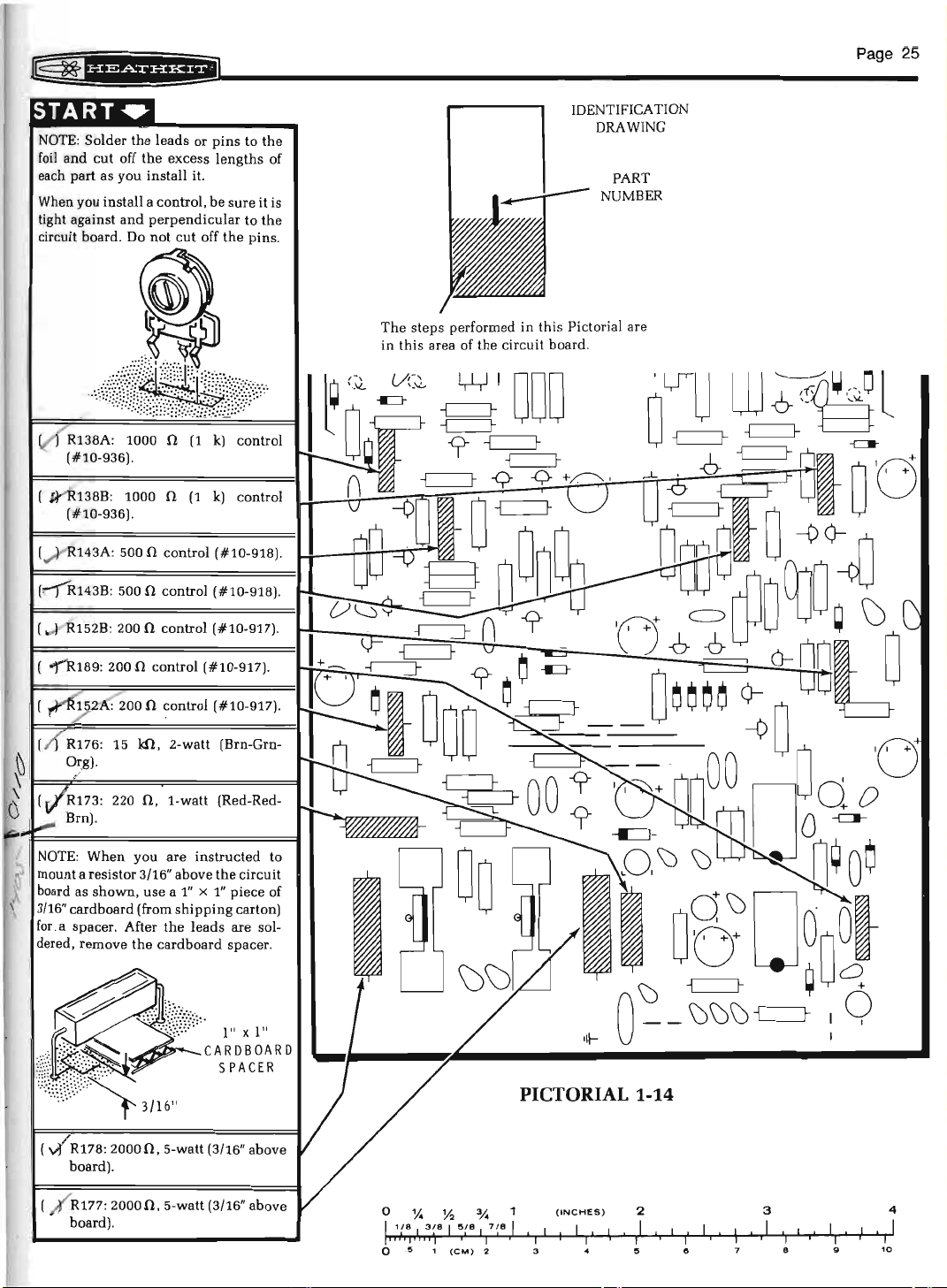
NOTE
foil
: Solder
and
cut
off
the
the
leads or
excess
pins
lengths
each part as you install it.
When you install a control, be
tight against
circuit board. Do
(
~
and
138B
:
1000 0
perpendicular
not
cut
off
(1
k)
(#10-936).
(
.,....l
143A: 500 0 control (#10-918) .
sure
the
control
to
to
pins
the
it
the
of
is
Page
25
IDENTIFICATION
DRAWING
PART
NUMBER
.
The
steps performed in this Pictorial are
in
thi
s area of
the
circuit board.
(!"'")R.143B: 500 0 control (#10-918).
152B: 200
0 control (#10-917) .
200
0 control (#10-917).
15
kn
, 2-watt (Brn-Grn-
220 0 , 1-watt (Red-Red-
you are
instructed
mount a resistor 3/16" above
board as
3/
for
dered , remove
shown, use a 1" x 1"
16"
card
board (from
. a
spacer
. After
the
cardboard
~
or--
shipping
the
leads
the
CARDBOARD
circuit
piece of
carton)
are sol-
spacer
X 1"
1"
SPACER
to
.
•II-
PICTORIAL 1-14
R178:
board) .
R177:
board).
20000
, 5-watt (3/16" above
20000
, 5-watt (3/16" above
0
I
0
I I
1(8
fl
y.
I
j I I I
.5
%
!S(B
3~8
I
I
')
1
(CM)
"4
1;8
I
I
2 3 5
(INCHES)
1
I I
I
I
I I I I
I I
I
4
I
I
I
I
10
I I
I
I
3
I I
I
I
I
I
I
8
"
2
I
I
"
Page 28

Page
26
Refer
toPictorial1-15
the
following steps.
NOTE:
circuit
pin 1 end
the
(
( ) Q101B: Install a 5566
(
When
(I
circuit board. See
~
Q101A: Install a 5566
location Q101A .
location Q101B.
-1
Q102A: Install a 5566
location Q102A.
C)
of
in
you
the
the
(Illustration Booklet, Page
install a transistor
following steps,
transistor
or
Detail1-15A.
( j Q102B: Install a 5566
/ location Q102B.
( ) U102: Install a
I U102.
7472Ic:;
or
integrated
be
sure
to
match
IC
to
the
index
transistor ( #417
transistor
transistor
transistor ( #417
(#443-4)
(#417-902)
(#417-902) at
at
3)
for
the
mark
on
-902)
at
at
-902)
ar
location
2.
Fit
the
pins
of
into
control
down
turn
the
end
these
against
If
they
the
switch
all
the
foil.
rotary
you
step, cut
length
their
switch
and
time,
and
switch
3. Carefully
only
spect
are
tight
board.
push
solder
to
the
(
'-')
/ SW2A - R3A: In
other
(#63-1316) at its location
the
When
next
end
.
NOTE:
in
indicated
each
each
switch
board
holes
pins
are
in
tight
against
the
circuit
pins
of each wafer
pins
the
printed
are not,
remaining
switch
are
reheat
tight
against
the
same
with
instructed
the
specified color
remove 1/4" of
wafer,
place.
the
board
to
make
switch
manner,
5000 0
on
to
one
until
all
Then
circuit
over
to
sure
side
of
the
connection
the
and
(5
the
circuit
prepare
insulation
wafer at a
the
push
board.
and
the
foil. In-
all
the
the
board.
control
install
k)
control
board.
wires, as
wire
switch
the
solder
pins
circuit
and
Then
pins
the
to
the
from
(
~
U101:
U101.
(
SW2B-
/
rotary
1316)
circuit
1. Carefully
with
Install a 7400
switch
at
board
their
IC
R3B: Refer to
with
5000 0
its
location
as follows:
align
the
pins
holes
in
the
SMALL
(#443-1) at
Detail1
on
the
of
circuit
5B
(5
k)
printed
the
front wafer
board.
location
and
mount
control
side
(#63-
of
the
(A)
DOT
a
·~~~~
ulf)~
PIN1 PIN1
~
PIN
Detail1-15A
Prepare
are
RIDGE
listed
the
in
3"
2"
NOTCH ___
~~
PIN
1
following
the
3"
2-1/4"
0{1
pIN
1
~
order
.
brown
they
--
~
wires.
The
will be used.
<
~~
wires
Page 29

Page
27
I§~
f§fifi*U*FP
NOTES:
1.
When
board, always
after
in
2.
solder
later.
means
number
wires are
3.
When you
sure
directly above
capacitors, as
justed later.
j
Connect a 3"
( )
(S-1)
tion
the
spacer
you
connect a wire
cut
the
connection
the
following steps, (NS)
because
"S-"
to
other
with a number,
solder
following
at
the
connection.
wire
to
no
wires or
components
the
these
Brn
wire
to
switch
on
wire
the
SW2A
between
switch.
off
the
excess
is soldered.
wires
the
connection.
the
"S"
tells
the
rotary
screws
in
trimmers
from
circuit
wafer A lug
the
shaft
to
the
circuit
lead
length
means
will
such
not
be
added
as (S-3),
how
switches,
are
positioned
the
trimmer
must
be
board
hole
9 (NS). Posi-
and
indicated
to
The
many
be
ad-
A
C
v(
Connect a 2"
A2 (S-1) to
(J Place a 1/2"
0 , 1/2-watt (Org-Org-Blk)
33
/)['
R2A:
tween
switch
length
Connect
wafer A
(S-1).
(
~
R106A: Connect a 33
5%
resistor from
in
the
circuit
B
lug
9 (S-1).
(
~
onnect
CC
Position
indicated
V )
Connect
hole
(S-1).
the
~
33
(~B:
tween
~
S-1).
(
v('
R106B: Connect a 33
5%
on
B
(
~
a
3"
(S-1) to
switch
the
spacer
a 2-1/4" Brn
B2
(S-1) to
Position
indicated
/2"
length
0,
1/2-watt (Org-Org-Blk)
Connect
wafer A lug
resistor from
the
circuit
lug
9 (S-1).
t
the
circuit
Brn
wire
from circuit
SW2A wafer A lug 8 (S-1).
of sleeving
on
5%
this
lug
the
board
Brn
wire
resistor to
9 (NS)
0,
indicated
(S-1) to
switch
and
wafer B
1/2-watt (Org-Org-Blk)
resistor
switch
from circuit
SW2B wafer A
wire
between
on
switch
the
wire
spacer
of sleeving
the
on
the
shaft
switch.
wire
from
SW2B wafer A
between
the
the
switch.
on
each
5%
this
the
board
board
resistor ! o
9~')
0,
indicated
(S-1) to
aside
switch
and
wafer B
1/2-watt (Org-Org-Blk)
resistor
switch
temporarily
board
hole
each
lead
of a
resistor.
SW2A be-
lug
outline
SW2A wafer
board
lug
circuit
hole
9 (NS).
and
board
the
lug
shaft
and
lead
of a
resistor.
SW2B be-
lug
outline
SW2B wafer
.
8
8
8
Q .5 1
(C
M ) 2
'II
7
I
17
(INCHES)
'I
I I
II,
3
2
. I '
I
·,
I
I '
s
"
3
' I .
'I
4
, I ,
I I
8
' I
I I'
I
10
9
I, ' I'
11
5
'• I I
12 13
6
I I
I ' I
I''
,.
I '
I
1tl
1S
Page 30

Page
28
Refer to Pictorial 1-16 for
~
(
Locate
shown.
the
switch
I SW1A: Install a DP3T
location
x 1/4"
stalled
( .;{ SW1B:
3-position
switch
NOTE:
refers
use
hardware,"
screw,
Refer
number
install
nished
start
The
to
to
mount
one
to
the
with
them
SW1A
flat head screws.
either
In
the
slide
bracket.
term
"hardware"
the
screws,
parts.
for example,
or
more
the
Detail called
of
lockwashers
hardware. Use
the
kit
on
screws.
in
the
way.
same
switch
nuts,
The
#4
lockwashers
to
to
pick
the
following steps.
bracket
3-position
switch
The
manner,
at
location
in
the
and
lockwashers
phrase
means
out
in
use
the
up
to
the
and
plastic
#4
and
position
slide
bracket. Use 6-32
switch
install
SW1B
following
"Use
4-40 x 1/4"
use
a 4-40 x 1/4"
and
a 4-40
step
for
the
correct
nut
and
#6
it
switch
can
be
a DP3T
in
steps
you
will
nut.
the
correct
way
starter fur-
nuts
and
as
at
in-
the
to
switch
switch
Now
against
drawing
J1
: Install a BNC
switch
furnished
J2:
(
~
Refer to
the
( J)
-
~
In
at
location
Refer
bend
shown.
Pictorial1-17
following steps.
Prepare
Remove
from
bracket.
with
4-40 x 1/4" flat
bend
the
switch
the
bend
#1
on
bracket. Use
with
the
same
J2
in
to
inset
drawing
the
indicated
two
2"
an
extra 1/2" (total 3/4") of
one
end
of
Secure
in
Pictorial1-16.
connector
the
manner,
the
(Illustration Booklet, Page
brown
both
the
tab,
that
the
switch
at
the
lockwasher
connector
install
switch
#2
on
lugs
on
wires.
2"
brown
other
tab of
head
hardware.
is
in
the
bracket.
location
and
a BNC
bracket.
Pictorial1-16
switch
See
a 3/8" spacer.
connector
insulation
wires.
the
slot, flat
inset
J1
in
the
and
nut
and
SW3 as
4)
for
SW3:
switch
Push
into
either
the
tab of a DP4T
slot
at
location
4-position
SW3
slide
in
the
Page 31

13-1/2"
1/4"
MARK
WITH
INK
MARK
WITH
INK
Page
29
Connect
(
j)
these
Pass
the
through
other
end
( 1 Pass
(
v)
the
wire
through
the
other
Locate
the
cable for its full
conductors. Discard
consisting
ductors
( \1) Refer
the
0
y.
11
!8 I 3 ( 8
iihjlilij
.5
1
0
13-1/2"
y,
5fe
I
I
(C
M)
, as it will
to
•;.
718
I
I I I
I
2 3
two
wires
to
longer
lug
longer
end
bared
9 (NS) to
of
this
bared
lug
of
wire
8 (NS)
this
8-conductor
length
of
the
Grn, Blu , Viol ,
not
Detail 1-17 A
length
I I I
of
(INCHES
0
I
I
I
switch
end
lug
to
end
wire
SW3 as follows:
of
one
4 (S-1).
lug
6 (S-1) .
of
the
to
lug
7 (S-1).
to
lug
5 (S-1).
2"
Connect
other
flat cable. Separate
between
the
the
Yel
4-conductor
and
be
used.
and
prepare
4-conductor
)
2
I I I
I
I
I
5
the
flat cable.
I
I
..
1/4"
Brn
wire
the
2"
Brn
Connect
this
and
Grn
section
Gry con-
ends
3
I
I
I
I
8
of
I
NOTE: Where a wire passes
goes
to
solder
ing
connections
"through
Connect
has its
(
~
( { Org to
( 1
(
..{
The
I I
I I
I
I
9
another
instructions
the
connection.
ends
Yel to
ed
Brn
free
4
I I I I I I I I I I
I
10
, to
wires."
the
end
even, to
lug
lug
to
lug
to
lug
end
of
I
I
,
point, it
this
will
(S-2), one
Be
sure,
apply
of
enough
this
switch
10 (S-1) .
9 (S-3).
8 (S-3).
3 (S-1).
cable
5
I
I
I
12
13
through a connection
count
as
two
wires
entering
when
heat
4-conductor
and
you
solder
to
solder
flllt cable,
SW3 as foi lows:
will
be
connected
6
I
I I I I I I I I
I
I
I
I
15
1.
I
16
one
later.
and
in
the
leavthese
these
that
I
17
7
I
Page 32

Page
30
~I
~
~~
~
~
~
~~-iL~-
-
:
Q
I n I
I-~
-1=~-~=---
~
Pl
r------..o
VERT I CAL
CIRCUIT
BOARD
~r~~~
J
I--~
Detail 1-17B
3/8-32
~
NUT
~I
~
Q
~-~~
ljll
n
m
~~I
Cliiiii-,..JJJ~
r!l·~
~
~~~
-t?-~
4-CON
FLAT
m¥~
-1~
DUCTOR
CABLE
m I
(J Refer to Detail 1-17B
bracket
(mounted
3/8-32 nuts. Be
switch
cable above
Connect
the
circuit
Org to hole T (S-1).
Brn to
Yel to
Red
Prepare
Connect
lug 7 (S-1) to
onto
bracket as
the
free
board
hole
holeS
to
hole X (S-1).
two
a 1-3/4" Brn
switches
on
the
vertical
sure
to
shown
the
board. · -.:..:r
end
of
the
as follows: /
P (S-1).
(S-1).
1-3/4"
brown
circuit
and
mount
SW2A
circuit
position
4-conductor
wire
board
and
wires.
from
hole
the
the
the
switch
and
SW2B
board)
flange of
4-conductor
flat cable to
switch
B (S-1).
with
SW1A
the
,J
~
)
Position
fl
.-
~
~
~
\\
11\0
( Place a 3/8"
(
vJ
Connect
lug
uit
two
R1A:
to
(S-1).
lug 9 (S-3).
R1B: Connect one
to
(S-1).
circuit
shown.
a 1-3/4" Brn
3 (S-1) to
these
board.
33
0,
Connect
switch
Connect
switch
Connect
board
circuit
two
length
1/2-watt (Org-Org-Blk)
one
SW1A
the
Position
SW1B
the
(S-1).
wire
from
board
hole
wires
down
of sleeving on
lead
of
one
through
other
lead
through
other
lug
lead
the
resistor as
of
the
lug
lead
Position
other
switch
BB
against
each
5%
of
these
3 (S-2) to
to
switch
shown.
33 0 resistor
7 (S-2) to
to
hole AA
the
resistor as
SW1B
(S-1).
the
lead of
resistors.
resistors
lug
SW2A
lug
in
cir-
6
2
the
0
y.
I 1(8 I 3f8
iifljiiiif
5
0
1
(INCHES
)
3f.
Y:.
7 / 8
5(8
I
I
1
(C
I
M ) 2
I
I I I I
I
I
I
I
3
2
I
I I
I
I
'
I
I
5 6 8
I I
I
3
I
I
'
I
I
I
I
I
I
I
I
I
9
4
I I
I I I I I
I
10
I I
I
,
I
5
I
I
I
I
I
12
I
I
13 14
I
I
6
I I I
I I I
I
I
1~
"'
I
7
I
I
I
I
17
Page 33

4-40
#4
LOCKWASHER
NUT
@__~
Page
31
NOTE:
the
rial1-17.
(..--1
( efer
Be
sure
to
next
two
steps,
/
C1:
Connect
through
through
ther
ard
C2:
through
through
her
e
grooves
4 X3/8" screw.
Refer
transistor (#417-834)
1/4" hardware. Be
transistor
connector
lug
lead
the
band
Connect
connector
lug
lead
band
to
Detail 1-17C
in
to
Detail 1-17C
position
exactly
one
1 (S-2)
to
switch
on
one
5 (S-2)
to
switch
on
the
the
bottom
are
positioned
the
capacitors,
as
they
lead
of
J1
(S-2)
to
lug
SW1A
the
capacitor.
lead
of a
J2
(S-2)
to
lug
SW1B
capacitor
and
of
and
on a heat
sure
the
installed
are
shown
.1
J.LF
Mylar
to
switch
5 (S-1).
.1
J.LF
1 (S-1).
lug
.
both
install
beveled
as
Connect
lug
4 (S-1). Disre-
Mylar
to
switch
Connect
8 (S-1). Disregard
prethread
heat
sinks. Use a
an
sink
with
edges of
shown.
in
in
Picto-
capacitor
SW1A
the
capacitor
SW1B
the
the
two
MPSU10
4-40 x
the
·
/
)
In
the
same
transistor
Q115:
lead of
and C leads
sponding
at
circuit
solder
the
(
~
Q116:
transistor
Q116
Refer to Detail 1-17D
circuit
holes
the
flat
Then
shield
Place a short
one
location
board
the
excess
In
on
board
and
printed
4-conductor
turn
tabs
Detail
manner,
(#417-834)
of
these
of
the
E,
B,
and
Q115.
with
transistor
lead
lengths.
the
same
and
short
the
circuit
shield
push
the
side
of
cable is
the
circuit
to
the
foil.
1-170
install
on a heat
ferrite
transistors. Insert
transistor
C holes
Secure
two
leads
manner, install
ferrite
board.
and
into
shield
the
circuit
board
another
sink.
bead
into
in
the
the
heat
#4
x 3/8" screws.
to
the
foil
bead
insert
the
their
down
board
positioned
over
and
MPSU10
on
the
theE,
their
circuit
sink
and
the
at
location
tabs
circuit
tight
. Be
as
solder
center
correboard
to
the
Then
cut
other
on
the
board
against
sure
the
shown.
the
B,
off
Page 34

Page
32
RefertoPictorial1-18 (Illustration Booklet, Page 5) for
the foLlowing steps.
(/
Turn
the
it as
shown
(
_)
Refer
to
bracket at
6-32
x 1/4" hardware.
;(
In
the
same
bracket
at
V R4B: Refer to
(1
k)
control
at
location
control so its
( R4A:
/
In
the
control (#10-1118)
circuit
Detail 1-18A
location
board
foil
in
Pictorial 1-18.
R4B
manner,
mount
location R4A
Detail1-18A
(#10-1118)
R4B
with
a 3/8-32
lugs
are
same
manner,
on
side
up
and
mount
on
the
circuit
the
on
the
and
mount a 10000
on
the
nut.
up
as
shown.
install
the
control bracket
and
a control
board. Use
other
circuit
control
Position
a 1000 n
position
control
board.
bracket
(1
location R4A.
NOTE:
When
lowing steps,
touch
the
v{
R12B:
Red)
/
the
(
-/
) R119B:
Red)
9fe
(
~
R121A:
Red)
the
/
(/ R119A:
Red)
the
(~Prepare
NOTE:
circuit
above
the
tion
to
Connect a 2"
(S-1)
do
metal
Connect
5%
indicated
Connect
5%
indicated
5%
indicated
5%
indicated
When
board,
foil to
the
wire
to
the
you
wire
these
not
allow
case of
the
a 3300
resistor
from control
hole
a 3300 n, 1/2-watt (Org-Org-
resistor from
hole
Connect
a 3300
resistor from
hole
Connect
a 3300 n, 1/2-watt (Org-Org-
resistor from
hole
two
2"
brown
you
connect a wire
keep
the
be
sure
you
and
circuit
Brn
wire
indicated
two
controls
any
of
the
controls.
0,
1/2-watt (Org-Org-
in
the
circuit
control
in
the
circuit
0,
control
in
the
circuit
control
in
the
circuit
wires.
insulation
get a
good
board
from control
hole
in
in
the
fol-
resistor
R4B
R4B
lug
board
lug
board
leads
1 (S-1)
(S-1).
3 (S-1)
(S-1).
1/2-watt (Org-Org-
R4A
lug
1 (S-1)
R4A
to
board
the
on
solder
lug
board
foil
the
wire
(S-1).
3 (S-1) to
(S-1).
side
of a
1/8"
connec-
foil.
R4B
lug
the
circuit
board
(S-1).
the
k)
at
to
to
to
to
2
Connect a 2"
to
(S-1)
the
indicated
Brn
wire
from control R4A lug 2
hole
(S-1).
CIRCUIT BOARD CHECKOUT
Carefully
conditions.
( ) Diodes for
( ) IC's for
There
board
aside temporarily.
Save
The
Save
inspect
Unsoldered
solder
Poor
Solder
Protruding
Transistors
the
connections.
connections.
bridges
leads
for
circuit
between
which
the
proper
Electrolytic capacitors for
of
the
positive
tion
of
the
the
are a
number
that
will
the
remaining
following
them
3 6-32
4 6-32
3
Slide
parts
for
use
x 1/8"
x 1/8" setscrews
switch
1 Metal front
5"
extension
2
2
Split
plastic
couplings
Shaft
2
knob
Red
1
2 Small
1 Large
1
1
1
1 Cable
2
black
black
Sleeving
Shielded
Label
assembly
Alligator
2 Alligator
(
the
proper
banded
proper
of
be
used
parts
should
later.
black
covers
panel
shafts
bushings
knobs
knob
cable
clips
clip
insulators
+)
or negative
end.
type
unused
later. Set
setscrews
with
board
foil patterns.
could
type
type
and
for
use
be left over at
connector
in
the
circuit
for
the
touch
and
installation.
the
correct
(-)
and
the
correct posi-
installation.
holes
in
the
circuit
later.
board
following
together.
position
end.
the
circuit
board
this
time.
IIFipiiij
Q 5 1
I I I
(CM)
7
I
I
II
17
12
5
II
I I I I I
6
I I
I I
I. I I
I I
I
I
13
14
,.,
15
(INCHES)
I I I I
2
Ill
2
·~
I I
I
I
5 8 9
3
I I
I I I I I
I I I
I I
I
10
4
I I I I I
I I I
,,
Page 35

HORIZONTAL
CIRCUIT BOARD
PARTS LIST .
Remove
each
correspond to
Board Parts Pictorial (Illustration Booklet , Page 6).
part
the
parts
against
from
the
the
numbers
the
pack
marked
following list.
on
the
#2
and
check
The
key
numbers
Horizontal Circuit
To
order a replacement
PART NUMBER. Use
with
the
kit.
If
one is
Parts" i
separate
nside
"Heath
the
rear
Parts Price List."
part, always
the
Parts
not
available, see "
Order
include
Form
Replacement
cover. For prices, refer
Page
33
the
furnished
to
the
KEY
HEATH
No. Part No.
RESISTORS
All
resistors
(fourth
NOTE:
velope
pack
band
The
(stamped
before
are
silver).
resistors
you
1/2-WaH
A1
6-279
A1
6-100 3
A1
6-470
A1
6-221
A1
6-271
A1
6-331
A1
6-391
A1
6-511
A1
6-561
A1
6-821
QTY.
5%
RES).
check
DESCRIPTION
(fourth
band
gold)
unless
designated
may
be
packed
Open
all
the
resistors
2.7
!1
5
2
8
2
2
1 390
2
2 560
(Red-Viol-Gold)
10
!1
(Brn-Bik-Bik)
47 n (Yei-Vioi-Bik) R214, R215
220
!1
(Red-Red-Brn) R230, R237,
270
!1
(Red-Vioi-Brn) R212, R255
330
!1
(Org-Org-Brn) R209, R228
!1
(Org-Wht-Brn) R229
510
!1
(Grn-Brn-Brn) R206, R207
!1
(Grn-Biu-Brn) R235, R258
820
!1
(Gry-Red-Brn) R217
the
in
more
resistor
against
than
envelopes
the
Parts
CIRCUIT
Comp.
No.
10%
one
en-
in
this
List.
R241
, R275,
R276, R277,
R281
R244, R269,
R270
R238
, R246,
R253, R254,
R259, R260
KEY
No
HEATH
Part No.
.
QTY.
Resistors (Cont'd.)
A1
6-102
A1
6-152 1 1500
A1
6-182
A1
6-222 2200
A1
6-682 6800
A1
6-103 10
6-153
A1
A1
6-473 2 47
A1
6-683 1
6-104
A1
6-684
A1
A1
6-914 910
A1
6-105 1
1-163
A1
A1
1-166 10
13
5
1
5
DESCRIPTION
1000
!1
(Brn-Bik-Red)
!1
(Brn-Grn-Red)
1800
!1
(Brn-Gry-Red)
!1
(Red-Red-Red)
!1
(Biu-Gry-Red)
k!1
(Brn-Bik-Org) R256
15
k!1
(Brn-Grn-Org)
k!1
(Yei-Vioi-Org) R220,
68
k!1
(Biu-Gry-Org)
100
k!1
(Brn-Bik-Yel)
680
k!1
(Biu-Gry-Yel) R224
k!1
(Wht-Brn-Yel)
M!1
(Brn-Bik-Grn) R280
6.8
M!1
(Biu-Gry-Grn) R223
M!1
(Brn-Bik-Biu)
CIRCUIT
Comp.
R272
R226
R225
No.
R12, R202,
R204, R218,
R221
R219,
R227, R245,
R262,
R268
R273, R278,
R282
R248
R205,
R208
R213, R216,
R250
R210
R222
R201
, R239,
R243,
R252
R274
R242
R240
,
,
,
,
Page 36

Page 34
KEY HEATH
No.
Part
QTY. DESCRIPTION
No.
Other Resistors
1-21-1
A2.
A3 1-23-2 2 5600
A4 5-2-2 2 22
n' 1-watt, 1 0%
680
(81u
-Gry-8rn)
n, 2-watt R263, R265
(Grn-81u-Red)
k!l
, 2-watt R233, R264
CAPACITORS
Ceramic
81
21-157 5
21-7
81
81
21-32
81
21-121
81
21-75 100 pF C212
21-21
81
81
21-56 1 470 pF C214
81
21-36
81
21-16
81
21-82 1
81
21-199
pF
1 33 pF C204
47
pF
2
pF
2 56
200 pF C222
3
.002
JLF
01
.02
.1
JLF
JLF
JLF
2 .
3
Tantalum - Electrolytic
C1
25-221 1
25-820
C2
C2 25-115
C2 25-233
2
9
JLF
tantalum C208
2.2
10
JLF
NP (non-polarized) C203, C221
electrolytic
10
JLF
electrolytic C206, C217,
JLF
electrolytic C207
22
Other Capacitors
CIRCUIT
Comp. No.
R232
C219
C220,C235
C205, C213
C211, C218,
C229
C202, C224
C210
C209, C228,
C232
C223, C225 ,
C226, C227 ,
C230, C231 ,
C234
KEY HEATH QTY. DESCRIPTION
No. Part
-------
No.
CIRCUIT
Comp.
DIODES
56-56
01
01 56-59
56-67
01
TRANSISTORS
1N4149
8
1 1N750A
2 VR10A
INTEGRATED CIRCUITS
-
0201 , 0204
0207
, 0208,
0209
, 0210,
0213
, 0214
0206
0205
, 0211
(IC's)
NOTE: Transistors and integrated circuits are marked for iden-
tification in one of the following four ways:
1.
Part number.
2. Type number. (On integrated circuits this refers only
to the numbers and letters listed. Any additional
letters or numbers
3. Part number and type number.
4. Part number with a type number other than the one
listed .
E1
417-134
E2
417-154 1 2N2369 transistor
417-235 2 2N4121 transistor
E1
E1
417-801 4
417-834
E3
E4 417-902
E5 443-6 7474 IC U201
E5 443-22 74121 IC U205
E5 443-23 74122 IC U203
E5 443-44 7413 IC
443-625
E5
5
2
3
on
an IC are not significant.)
MPS6520 transistor
MPSA20 transistor
MPSU 1 0 transistor
5566 transistor 0201,
74132 IC
0209,
0212, 0213,
0217
0216
0203, 0204
0202,0205
0206
0214,
0208
U204
U202
0210
, 0211
0215
0207
No.
,
,
,
29-5 1 000 pF polystyrene C216
C3
27-47
C4
C5
27-2
.1
JLF
Mylar
JLF
film
1
C201
C215
Page 37

l§
KEY
No
. Part
~
f§f*Si¥fHil
HEATH
QTY. DESCRIPTION
No.
CIRCUIT
Comp. No
KEY
. No.
HEATH
Part
No.
QTY.
DESCRIPTION
Page
35
CIRCUIT
Comp. No.
CONTROLS
F1
F2
F1
F1
F1
10-918
10-391
10-936
10-398
10-904
2
HARDWARE
G1
G2
G3
G4
250-52
250-186
252-15
254-9
2 4-40 x 1 /4" screw
4
2 4-40 nut
2
MISCELLANEOUS
H1
H2
H3
H4
434-230
434-298
475-16
475-10
3
5
2
2
500
n control
1000 n ( 1
1 000
2000
5000
#4
#4
8-pin IC socket
14-pin IC socket
Short ferrite bead
Long ferrite bead
K)
control
n ( 1
K)
control
n (2K) control
n (5K) control
x 3/8" screw
lockwasher
R231
R236
R257
R251
R211
FB
FB
, R247
PARTS FROM FINAL PACK
J1
63-1315
85-2044-2
J2
215-95
344-51
344-163
344-165
344-166
344-167
344-168
344-56
344-170 1'
344-58
344-172 1'
344-173
344-174
344-175
344-176
344-177
344-178 1'
344-179
344-180
344-181
Rotary switch with 5
and 1 0
kO.
1
Horizontal circuit board
2
Heat sink
6'
-8
" Brn wire
2'
Blk wire
1' Red wire
1'
Org wire
1'
Vel wire
1'
Grn wire
2'
Blu wire
Viol wire
2'
Gry wire
Wht wire
1'
Wht-Bik wire
1'
Wht-Brn wire
1'
Wht-Red wire
1'
Wht-Org wire
1'
Wht-Yel wire
Wht-Grn wire
1' Wht-Biu wi
1'
Wht-Viol wi
1'
Wht-Gry wire
controls
re
re
kO.
SW5-R10-
R11
Page 38

Page
36
The
steps performed in this Pictorial are
in this area of
the
circuit board. ------¥.4"
START•
Position
up
NOTE: When you install a diode, al-
ways match
the
as
band
the
shown
on
circuit
.
the
band
the
board
on
circuit
printed
the
board
diode
.
STEP-BY-STEP ASSEMBLY
IDENTIFICATION
DRAWING
PART
NUMBER
side
with
201: 1N4149
0214
1"
bare wire.
1"
bare wire.
J)
1"
bare wire.
: 1N4149
diode
diode
( /1 1-3/8" Brn wire.
t-
)
Solder
the
off the excess lead lengths.
1"
"bare
1"
1-1/8" Brn wire.
1-5/8" Brn wire.
1-1/8"
Solder
off
leads to
bare wire.
wire.
bare wire.
Brn
wire
the
leads to
the
excess lead
.
(#56-56).
(#56-56).
the
foil
the
foil
lengths
and
and
.
cut
cut
1-1/8"
Brn
wire
1-3/4" Brn wire.
1-5/8" Brn wire.
1-3/8" Brn wire.
Solder
the
off
leads to
the
excess lead lengths.
1-7/8" Brn wire.
1-1/4" Brn wire.
1-1/2" Brn wire.
2"
Brn wire.
Solder
the
the
excess lead
leads to
off
.
the
foil
the
foil
lengths
and
and
.
cut
cut
II II I iII
Q .
'i I I I
!5
1
(CM
) 2
(INCHES)
, I I ,
I I
3 •
2
I
I
e
I I I
~~
I I
e
PICTORIAL 2-1
3
I I
7 8
I I I
I I
9
I I
I
10
4
I I I
I I 1 I
11
5
I.
I I
I.
12 13 14
I I I I
6
I I
I
"'
I I
17
7
I
I
Page 39

~
~
1
§f!di#B*+i
The
steps
performed
in
this
area of
·
the
in
circuit
this
board.
Pictorial
are
Page 37
IDENTIFICATION
DRAWING
PART
NUMBER
( /t"
I
1-3/4"
(
v{
0211:
(
v{
0208:
(
ij'
0207:
(
/)
0213
) 1-3/8"
I
Solder
off
bare
Brn
VR10
1N4149
1N4149
: 1N4149
Brn
the
the
excess
wire.
wire.
leads
diode
wire
diode
diode
diode
.
to
lead
(#56-67}.
(#56-56).
(#56-56).
(#56-56).
the
foil
lengths.
and
cut
PICTORIAL 2-2
(. I[D209: 1N4149
0210
: 1N4149
Solder the
off
the
excess lead
leads
diode
diode
to
the
(#56-56).
(#56-56).
foil
lengths
and
.
cut
2Z>D
Page 40

Page
38
The
in
kn
) R252: 100
R208: 1800
R212: 270
(Brn-Blk-Yel).
n (Brn-Gry-Red).
n (Red-Viol-Brn).
1
16: 1800
Solder
off
fJ R219: 1000 0 (Brn-Blk-Red).
the
the
leads
excess
n (Brn-Gry-Red).
to
lead
steps
this
the
lengths.
performed
area of
foil
and
the
cut
in
circuit
this
Pictorial are
board
IDENTIFICATION
.
DRAWING
PART
NUMBER
1000
R205: 1800
R210: 15
R209: 330
R214: 47
Solder
R217: 820
kn
0 (Yel-Viol-Blk).
: 1000
the
the
excess
n (Brn-Blk-Red).
0 (Brn-Gry-Red).
(Brn-Grn-Org) .
n (Org-Org-Brn).
0 (Brn-Blk-Red).
leads
to
the
foil
and
lead
lengths
0 (Gry-Red-Brn).
cut
.
R229: 390
R228: 330
R268: 1000
R277: 2.7
R278: 1000
R227: 1000
Solder
the
off
the
excess
n (Org-Wht-Brn).
n (Org-Org-Brn).
0 (Brn-Blk-Red).
0 (Red-Viol-Gold).
0 (Brn-Blk-Red).
0 (Brn-Blk-Red).
leads
to
the
foil
lead
and
lengths.
cut
PICTORIAL 2-3
R242: 910
R244: 10
R237: 220
R220: 47
LJ-Solder
(
off
kn
0 (Brn-Blk-Blk).
n (Red-Red-Brn).
kn
the
leads
the
excess
(Wht-Brn-Yel).
(Yel-Viol-Org).
to
the
foil
lead
11nd
lengths.
cut
Page 41

IDENTIFICATION
DRAWING
PART
-'l'A~--Th
e
steps performed in this Pictorial are
in this area of
the
circuit board.
Page
39
23: 6.8
MD.
24: 680
kn
74:100
kn
Solder
the
off
R262: 1000
R256: 10
leads to
the
excess lead lengths.
!l
kn
(Brn-Blk-Org).
5:
270
!l
(Red-Viol-Brn).
2:
1000 n (Brn-Blk-Red).
(Blu-Gry-Grn).
(Blu-Gry-Yel).
(Brn-Blk-Yel).
the
foil
and
(Brn-Blk-Red).
cut
II
16: 1000
the
capacitor
circuit
R225: 68
R226: 6800
pF
band
(colored end)
with
board.
kn
!l
!l
: 1000
220 n (Red-Red-Brn).
10
MD.
100
kn
polystyrene. Match
on
the
band
on
(Blu-Gry-Org).
(Blu-Gry-Red).
(Brn-Blk-Red).
(Brn-Blk-Blu) .
(Brn-Blk-Yel). /
.,..,
the
the
.../
_.A
R250: 1800
R248: 1500
) R270: 10
) Solder
off
the
the
excess lead
n (Brn-Gry-Red).
!l
(Brn-Grn-Red).
!l
(Brn-Blk-Blk).
leads
to
the
foil
lengths
and
.
cut
PICTORIAL 2-4
!l
560
!l
59: 220
Solder
the
off
leads to the foil
the
excess lead lengths.
(Grn-Blu-Brn).
(Red-Red-Brn).
and
cut
Page 42

Page
40
NOTE:
When
Pictorial, sol
the foil as
you install a
der
the
each
part
pins
is
part
of
each
installed
in
part
.
I~
this
to
!
(/J
8-pin
IC socket at Q201.
!v Y 8-
pin
IC socket at Q207.
8-pin
IC socket at Q208.
pin
IC socket at
14-
14-pin
IC socket at
14-pin IC socket at
R236: 1000
391).
!l
(1
0205.
0201.
0203
.
k)
control (# 10-
PICTORIAL 2-5
Page 43

Page 4
1
Q216: 2N236
154).
Align
th~
tor with
cuit
leads
holes of
the
cuit boar .
foil
lengths.
theta
board.
In~r
into
.t e.
the
Circu~~.
transistor 1/
d Solder
and
cut
~
LOCATIN t
G
TAB~~)/~
·
NO
align its
Insde
an b d
bove
a f
to
lengths.
h
Y
TE: W
rt
the
C holes. Position t e
the
the
01
~
ou
en
th
the
'
flat~
into
lea s h transistor
Then
oar . ff
'I
and
cut
FLA
(RI~OR
~~
.
.
..
9 transistor .
on
the
ta:tline
ot
ff
the
o
transis-
on
the
the
corresponding
board
above
the
excess e
I
cir-
C,
B'
and
E
.
Positi~n
the
Cir
-
leads
to
the
1
ad
I
"
:'=~f.G;
. II a transistor,
msta
their
o
.
}J~
fl t on
a E B
so lead
the
T'fE]
~~~f
. ·
.'·.',.;·:·:· :·'\ .
b ard
the
o .
cor~ect
lder
the
excess
{/4';
leads
.1/4"
·,.·
'')~
,
\
,'
,.~;l/f(~
( Q202:
tl
MPSA20 transistor
801).
Q203:
2
235).
Q206: M
801).
N4121 transistor
Q217:
(#417-134).
·01).
MPS6520
PSA20 transistor 11:
M
~~;.
',
Ji~
''
'
(#417
-
(#417-
(#417
-PSA20 transistor
0 (#417-
(#417-
PICTORIAL
2-6
Page 44

Page
42
The steps performed in this Pictorial are
in this area of the
JLF
C202: .01
CAUTION:
polarized
capacitors
capacitors
polarized capacitors have a positive
"
+"or
negative"-"
to use
an
specified
ic capacitors will be
in
ceramic.
There
are
both
and
polarized electrolytic
in
this kit.
are
NP capacitor
a step. All other electrolyt-
Nonpolarized
marked
marking. Be
the
polarized
non-
NP ,
when
type.
and
sure
it is
circuit
IDENTIFICATION
DRAWING
board.
PART
NUMBER
can
be
NOTE: NP capacitors
with either lead
C203: 10
C204:
C205: 56
NOTE: When you install a polarized
electrolyti c capacitor , always
the positive ( +) mark
with
the
cuit
board
mark on
(
-)
mark on
C225: 10
C234: 10
C217: 10
(
vf
C227: 10
( ) Solder
off
the
in
either
JLF
NP electrolytic.
33
pF
ceramic.
pF
ceramic.
positive ( +) mark
OR
match
the
capacitor
the
circuit
JLF
electrolytic.
JLF
electrolytic.
JLF
electrolytic.
JLF
electrolytic.
the
leads to
excess lead
hole
on
the
on
the
minus ( -)
with the
board.
the
foil
length
installed
.
match
capacitor
the
cir-
minus
and
cut
s.
- n_
When
capacitor (C231},
negative
capacitor
circuit
~-..0...• ~-.-----
1 capacitor
I
board
negative
board
"-"
lead
screen
......
- - • . - -
"-"
lead
you
install
insert
circuit
in
the
circuit
in
the
screen
C207:
22
the
the
positive"+"
board
positive
is
hole
circuit
incorrect
-----
board
positive
is incorrect.
JLF
electrolytic.
following electrolytic
lead
in
the
and
the
negative
boa d
hole
. !_he : ·
.
- ·
--
- ·
hole
circuit
and
bo
the
negative I
d hole.
--
The
1
-j
PICTORIAL
2-7
Page 45

START•
When
NOTE:
capacitor,
or
positive (
color
match
dot
+)
IDENTIFICATION
DRAWING
PART
NUMBER
you
install a tantalum
the
positive
on
the
capacitor
mark
on
l<l.;~~l~TR
the
board
(+)
with
·mark,
the
.
+
CONTINUEO
(
rrC
215: 1
J.L
the
capacitor
circuit
F film .
board.
on
the
Match
with
the
Page
the
band
43
band
on
C221: 10
C224: .01
Solder
the
off
the
excess
POSITIVE
J.LF
NP electrolytic.
J.LF
ceramic.
leads
to
the
lead
lengths.
MARK
foil
and
1+1
cut
12: 100 pF
680
33: 22
C222: 200
5600
5600
Solder
the
off
the
excess
ceramic
.
0 , 1-watt (Blu-Gry-
kO
, 2-watt.
pF
ceramic
.
0,
2-watt
(Grn-Blu-
0 , 2-wa
leads
to
lead
tt
(Grn-Blu-
the
foil
lengths.
and
cut
PICTORIAL
2-8
Page 46

Page 44
START•
NOTE: Solder
each
part
is
the
installed
pins
.
to
the
foil
as
~
R211 : 5000 n (5 k)
(
904).
(
.;
) R231: 500 n
( ) R247: 500
(J ) R251 :
( R257:
2000fi
398).
1000 n (1
936).
n
control
control
(2
k)
k)
control
(#10-918)
(#10-918)
control
control
(#10-
(#10
(#10
.
.
-
-
PICTORIAL
2-9
Page 47

Align
the
pin 1 end
index
mark
install
sistor.
on
each
.,:·
.
:::'~1'-~
'
':
.:·:
.'
:
:'~fJ#LI:
SMALL
I
~
PIN
1
the
circuit board
integrated
~
kr~.~
of
the
IC
with
PIN l
or
as
tran-
circuit
J-ND
::
,
l:f.\
{.'
:
:·
~i
~
the
you
Page
45
I ~
~~
PIN
l
Q201:
Q207:
2
oa
Q
02
02: 74132 IC
0204
)
0205: 74121
0201: 7474
0203: 74122
Pllll
5566
transistor
5566
transistor
:
5566
transistor
: 7413 IC
IC
(#443-625)
(#443
IC
(#443-22)
(#443-6)
IC
(#443-23).
f
~
.
(#417-902).
(#417-902)
(#417-902)
-44).
.
.
.
.
.
PICTORIAL 2-10
Page 48

Page 46
Refer to Pictorial2-11 (Illustration Booklet, Page
the
follow~ng
SW5-R10-R11: Refer to
the
controls ( #63-1315)
board
1.
Carefully
with
2.
Fit
time,
pins
Then
steps.
rotary
as follows:
their
the
pins
into
and
push
switch
align
holes
of
their
the
the
Detail2-11A
with
5000
at
its
the
pins
of
in
the
circuit
each
switch
board
holes
pins
of control R11 are
switch
down
!1
location
the
front wafer
board
wafer,
until
tight
and
(5k)
on
the
.
one
all
the
against
and
wafer
switch
in
circuit board.
3.
Carefully
only
spect
are
board.
push
solder
to
the
the
these
tight
If
the
all
foil.
turn
end
pins
switch
against
they
are not,
switch
the
remaining
the
circuit
in
pins
the
printed
tight
board
each
to make
reheat
against
switch
wafer
sure
side
the
the
and
over
and
to
the
foil. In-
all
the
of
the
connection
board.
control
Detail
7)
for
mount
10k
circuit
(A)
at
a
place
the
solder
pins
circuit
and
Then
pins
2-11A
( J)
( ) ) Remove
( )
.
")
(
Prepare
from
one
Connect
switch
(S-1).
cuit
SW5 wafer A
Connect
board
Remove
from
one
Connect
switch
(S-1).
Connect
cuit
board
the
following
brown
3-1/4" 3-1/4"
2"
2-1/4" 4-1/4"
2"
an
extra 1/2" of
end
of a 3-1/4" Brn wire.
the
longer
bared
through
the
other
end
hole
B9
(S-1).
an
extra 1/2" of
end
of a
2"
Brn wire.
the
longer
SW5 wafer B
the
bared
through
other
end
hole A9 (S-1).
wires:
3-1/4"
insulation
end
of
lug
5 (S-2) to lug 4
of this wire
insulation
end
of
lug 4 (S-2) to
of this
(total 3/4")
this
wire to
in
(total 3/4")
this
wire
lug
wire
in
cir-
to
5
cir-
0
I
0
1(8
II,,
5
I I
y.
I
3~8
it
(INCHES
a;.
Y2
7 / 8
5re
I
I
I)
1
(CM
I
I
I
I
I
I
I
) 2
I
3
)
2 3
I
I
I
I I I I
I
I
I
I
5 6 8
I I I I
I
I
I
I
I
I
9
I I
4
I I I I I
I
I
10
I
I
,
I
5 6
I
I
'
I
I
12
13
I
I
I
I
14
I
I
I
I I
I
I
"' "'
I
I I
7
I
I
I
17
Page 49

®
~
f¥f*SP#B*i?iJ
4-40
NUT
@_~
#4 LOCKWASHER
Page
47
(
~
onnect
wafer E
(
v(
Connect a 2"
/ lug 8 (S-1)
(/)
Connect
)
wleD9
(
~
Connect a 3-1/4"
j ole M (S-1)
M
Connect
holeD8
~~~
_:;---
Refer
to
following steps.
( ) / Prepare a
[
<Vj'
Connect a 3"
(S-1)
(
~
Connect
(S-1)
f/D
the
to
to
lug
(S-1)
(S-1) to
c;
inset
control
control R11
a 2-1/4"
to
a 3-1/4" Brn
a 4-1/4"
Brn
9 (S-1) to
Brn
wire
control
to
switch
Brn
to
switch
Brn
switch
./
\ "?
drawing
3"
and a 2"
Brn
wire
R11lug
a
2"
Brn
wire
wire
from
control
from
switch
Rll
lug
wire
from
SW5
waferD
wire
from
SW5 wafer E
wire
from
SW5
waferD
on
Pictorial 2-11 for
Brn
wire.
from
circuit
2 (S-2).
from
circuit
lug
3 (S-2).
switch
R11
lug
SW5 wafer E
2 (NS) .
circuit
lug
circuit
lug
circuit
lug
board
board
Detail 2-11B
SW5
3 (NS).
board
5 (S-1).
board
4 (S-1) .
board
4 (S-1).
the
hole
J
hole
I
Connect
R12:
resistor from
control
sleeving
Rll
on
a 1000
switch
lug
1 (S-1). Use a 5/8"
each
lead.
( 4 Refer to Detail 2-11B
grooves
#4
Refer
(
)V
transistor
1/4" hardware. Be
transistor
In
transistor (#417-834)
Q215: Place a
lead
and C leads
sponding
Q215.
with
transistor
lead
Q214:
transistor
Q21!
in
the
X 3/8" screw.
to
Detail 2-11B
(#417-834)
are
positioned
the
same
manner,
of
one
of
of
holes
Secure
two
#4
leads
lengths
In
on
the
and
the
.
circuit
bottom
sure
short ferrite
these
transistors.
the
transistor
in
the
the
heat
x 3/8" screws.
to
the
same
a short ferrite
0,
1/2-watt (Brn-Blk-Red)
SW5 wafer E
and
of
both
and
install
on a heat
the
beveled
as
install
on
a hea:t sink.
circuit
sink
foil
and
manner, install
board.
lug
prethread
heat
sinks. Use a
an
sink
with
edges of
shown.
another
bead
on
Insert
into
their
board
to
the
circuit
Then
cut
off
bead
at
5 (S-1)
length
MPSU10
MPSU10
the
at
solder
the
the
to
of
the
two
4-40 x
the
center
theE
, B,
corre-
location
board
the
excess
other
Iscation
Page 50

Page
Refer
48
to
Pictorial 2-12 for
the
following steps.
12"
Grn
wire
to
hole
E (S-1).
( ) Prepare
8"
Org
the
following wires:
6-1/2" Wht-Blk
6-1/2" Viol
6-1/2" Wht-Blu
4-1/2" Blk
later.
wire
end
to
Connect only one
the
horizontal circuit
connected
8"
Org
6-1/2" Wht-Blk
(
./)
6-1/2" Viol
(
;;
6-1/2" Wht-Blu
/(
4-1/2" Blk
(
(J )
8"
Red
wire
wire
wire
to
( j ) 7-1/2" Wht-Viol
8"
Red
7-1/2" Wht-Viol
9-1/2" Wht-Yel
9-1/2" Wht-Gry
of
each
of
the
following
board. Their
hole
K (S-1).
wire
to
to
hole
wire
to
to
hole(~)
hole
B (S-1).
wire
to
hole
AA
hole
hole
free
L (S-1).
(S-1).
BB
ground
N (S-1).
ends
(S-1).
(S-1).
wires
will
to
be
12" Wht-Org
12" Wht-Red
12"
Remove
one
gray
of each
two
Connect
the
foil
ends
will
10" Blu
Wht
end
prepared
steps.
only
side
be
wire
wire
wire
to
an
extra 1/2" of
(total 3/4") of
wires. Pass
wire
through
one
end
of
the
horizontal
connected
wire
with
to
hole
F (S-1).
to
holeD
hole G (S-1).
insulation
the
remaining
the
the
ferrite
of
the
two
circuit
later.
a long ferrite
(S-1).
9-1/2" Gry
Xl
(S-1).
wire
with
a long ferrite
CIRCUIT BOARD CHECKOUT
Carefully
inspect
the
circuit
board
conditions.
(S-1).
from
only
blue
and
longer
bead
bared
in
the
end
next
following wires to
board.
for
bead
bead
the
Their
free
to hole
X2
to hole
following
(
~
(
1'9-1/2"
( ) Prepare
Connect
the
horizontal
connected
~
)
Jil
ij
II II
Q .5 1
9-1/2" Wht-Yel
Wht-Gry
the
following wires:
7"
Wht-Brn
8"
Wht-Grn
9"
Brn
8-1/2" Yel
12" Grn
only
one
end
circuit
later.
8"
Wht-Grn
7"
Wht-Brn
9"
Brn
8-1/2" Yel
1 I I I
(CM)
wire
2
wire
wire
to
wire
I I I I
3
wire
to
hole
wire
to
hole
12" Wht-Org
12" Wht-Red
12"
Wht
10" Blu
9-1/2" Gry
of
each
of
the
board.
hole
to
(INCHES)
Their
to
hole
to
hole
EXT (S-1).
hole
Ill
P (S-1).
Q (S-1).
R (S-1).
C (S-1).
A (S-1).
following
free
ends
I I
e
wires
to
will
be
3
0 I 0 I 0
I I I
8
Unsoldered
Poor
solder
Solder
Protruding
Transistors
Electrolytic capacitors for
of
the
( ) Diodes for
tion
of
( ) IC's for
There
board
aside
Save
1
I I
1
9
are a
that
temporarily.
the
remaining
4 5
I 1
1
10
11 1'2
connections
connections.
bridges
leads
for
positive (
the
the
banded
the
proper
number
will
be
~
I,
,
1
1
1
between
which
the
proper
+)
end.
proper
end.
type
of
unused
used
later.
parts
,,
I
1
1
13
type
for
,.
.
foil
patterns
could
type
the
and
and
installation.
holes
Set
use
later. J
\ ,
,1
14
touch
and
installation
correct
the
correct posi-
in
the
circuit
6
~
,
I 1
1
1~
.
together.
position
the
circuit
board
~
, J ,
1
HS
1
1
11
.
j
1
I
1
Page 51

ORG
:::;;~L~K===-
~OL
=
~T-
--==~
=WHT-GRN
BL
U
RED
WHT-VIOL
WHT-YEL
WHT-GRY
W HT-
BR
N
-==---
---======F~
Page
49
GRN
==
W H T
OR
G
WHT-RED
WHT
PICTORIAL 2-12
BLU
GRY
Page 52

Page
50
POWER SUPPLY
CIRCUIT BOARD
Open
the
pack
the
following
numbers
Pictorial
marked
list.
on
the
(Illustration
#3
The
key
Power
Supply
Booklet, Page
and
check
numbers
each
correspond
Circuit
8).
part
Board
PARTS LIST
against
to
the
Parts
To
order a replacement
inside
the
"Heath
rear
Parts
cover.
Price
part,
For
List."
see
prices,
"Replacement
refer
to
the
= :
11
Parts"
separate
QTY
KEY
No
.
HEATH
Part
No.
. DESCRIPTION
CIRCUIT
Comp. No.
RESISTORS
All
resistors are
5%
(fourth band
gold)
unless designated 10%
(fourth band silver).
NOTE
: The resistors may
velope (stamped RES). Open
be
packed
all
in
more than one en-
the resistor envelopes
pack before you check the resistors against the Parts
1/2-Watt
A1
6-510
A1
6-471 470
A1
6-511 510
A1
6-
561
A1
6-102
A1
6-152
A1
6-182
A1
6-222
A1
6-432
A1
6-472
A1
6-562
A1
6-682
A1
6-103 10
A1
6-123
A1
6-153
A1
6-183
A1
6-273
A1
6-473
51
n (Grn-8rn-81k)
fi
(Vei-Viol-8rn)
fi
(Grn-8rn-8rn)
fi
(Grn-81u-8rn)
560
1
1000 n (8rn-81k-Red)
3
1 1500
3
1 5600
2 6800
1 12
2 15
2 47
n (8rn-Grn-Red)
1800 n (8rn-Gry-Red)
2200
fi
(Red-Red-Red) R317
fi
(Vei-Org-Red)
4300
4700
n (Vel-Viol-Red) R315
n (Grn-81u-Red) R316
fi
(81u-Gry-Red) R335, R336
k!l
(8rn-81k-Org)
k!l
(8rn-Red-Org)
k!l
(8rn-Grn-Org)
18
k!l
(8rn-Gry-Org)
kfi
(Red-Vioi-Org)
27
k!l
(Vei-Vioi-Org)
R322
R332
R325
R307
R311
R320
R341
R312, R313,
R342
R334
R331
R326
R328, R329
R321
R327
R318, R338
in
this
List.
, R314,
No
QTY.
.
KEY
No
.
HEATH
Part
Resistors (Cont'd.)
A1
6-104
A1
6-474 470
A1
6-105
3
Other Resistors
A2
1-30-1
A2
A2
A2
A3
1-32-1
3-5-2
3-11-2
5-1-3
3
CAPACITORS
Ceramic
81
21-33
81
81
81
21-120
21-141
21-16
2 500 pF
DESCRIPTION
CIRCUIT
Comp.
100
k!l
(8rn-81k-Vel)
k!l
(Vel-Viol-Vel)
1
M!l
(8rn-81k-Grn)
k!l
, 1-watt, 10% (Red-
220
Red-Vel)
k!l
, 1-watt, 10% (Vel-
470
Viol-Vel)
n,
2-watt, 10%
2.2
(Red-Red-Gold)
3.9
n,
2-watt, 10%
(Org-Wht-Gold)
2100 n (2.7
3-watt, 10%
3.3 pF C317
.0033
.
01
J.LF
J.LF
k!l)
,
R319,
R339
R324
R323
R308
R301, R309
R310
R302
R303
R306
C314,
C319
C318
No
R333
C315
.
,
,
Page 53

Page
51
KEY
HEATH
No
. Part No.
Other
Capacitors
B2
28-2
27-47
B3
B4
23-115
25-837
B5
25-288
B6
B7
25-241
QTY. DESCRIPTION
1 .1
3
3 1.5
1 25
4
DIODES
C1
56-26 1 1
C1
56-56
C1
56-89
C1
56-634 2 2EZ8205
C1
57-27
C1
57-52
7 1N4149
1 G0510
8 IN2071
2 007
1 pF phenolic (Brn-Bik-Wht)
JLF
Mylar
.1
JLF
paper
JLF
Tantalum
JLF
electrolylic
JLF
N191
electrolytic
(Brn-Wht-Brn)
1200
CIRCUIT
Comp. No.
C312
C316
C301
, C302,
C303
C309, C310,
C311
C320
C304, C305,
C306, C307
0314
0312, 0315,
0316, 0318
0319,
0320,
0321
0313
0311,0317
0303, 0304,
0305, 0306
0307, 0308 ,
0309, 0310
0301, 0302
QTY.
KEY HEATH
No. Part No.
TRANSISTORS-INTEGRATED
DESCRIPTION CIRCUIT
Comp. No.
CIRCUITS
(IC's)
NOTE: Transistors and integrated circuits are marked for identification
in
one of the following four ways.
1.
Part number.
2.
Type number. (On integrated circuits this refers only
to the numbers and letters listed. Any additional
on
an
IC
letters or numbers
are not significant.)
3. Part number and type number.
4.
Part number with a type number other than the one
listed.
01
417-237 2 SE6020 transistor 0301,
01
417-295 1
01
417-811 4
02
442-617
442-618
02
MPSL51 transistor
MPSL01 transistor
2 UA78 U301, U302
UA79
0302
0305
0303, 0304
0306, 0307
U303
MISCELLANEOUS
E1
E1
E2
E3
E4
E5
10-312
10-941
215-629
250-49
252-1
254-7
1 0
kn
control R340
1 00
kn control
3 Heat sink
6 3-48 x 1 /4" screw
6 3-48 nut
#3
6
lockwasher
R330
PART FROM FINAL PACK
E6
85-2045-1
354-7
1 Power supply circuit board
6 Cable tie
Page 54

Page
52
) R312: 1800 n [Brn-Gry-Red).
STEP-BY-STEP ASSEMBLY
The
steps performed
in
this area of
in
the
circuit board.
this Pictorial are
IDENTIFICATION
DRAWING
) R315: 4700
0315
Solder
off
the
n [Yel-Viol-Red).
: 1N4149
the leads to
excess lead
diode
diode
the
[#56-56).
[Brn-Wht-
foil
lengths
R336: 6800 n [Blu-Gry-Red).
1N2071
: 1N2071
der
the leads to
the
excess lead
n [Blu-Gry-Red).
diode
[#57-27).
diode
[#57-27).
the
foil
lengths
R335: 6800
0304:
0303
Sol
off
and
.
and
.
cut
cut
17:
off
the
0306:
)
0305
Sol
der the leads
off
the
2200
n [Red-Red-Red).
the
leads to
the
foil
excess lead lengths.
4300
n [Yel-Org-Red).
1N2071
: 1N2071
diode
diode
to
the
[#57-27).
(#57-27) .
foil and
excess lead lengths.
and
cut
cut
.
0
11{
0
ii
iljiiii)
.
8 I
~
14
Y:.
S(B
3~8
I
I
1
(CM)
%
I
7(8
I
I
2 3
PICTORIAL
{INCHES)
1
1
I
I
I
I
I
2
I
I
I
I
~
I I
I
I
I
e
3
I
I I
I
I
7
I
I
I
8
I
I
..
3-1
7
I
I
I
I
17
I
I I
I
I
"'
6
I
I
I
1e
4
I
I
I
I
10
I I
I
I
I
11
5
I
I
I I
I
I
I
12
I I
I
I
I
I
,.
13
Page 55

The
in
steps
this
performed
area of
in
the
circuit board.
this
Pictorial
are
r
IDENTIFICATION
DRAWING
:;:===
=======l
Page
53
. J J(
Is
R327: 27 k!l (Red-Vi ol-Org).
0318:
{
0319
(
tJ
0316
(
....-) R323: 1
/)
Solder
(
off
the
0310
0309
0308
1N4149
: 1N4149
: 1N4149
: 1N2071
: 1N2071
: 1N2071
1\1.0.
(Brn-Blk-Grn).
the
leads
excess
diode
diode
diode
to
lead
diode
diode
diode
(#56-56).
(#56-56).
(#56-56).
the
foil
lengths.
(#57-27).
(#57-27).
(#57-27).
and
cut
.342: 1800 n (Brn-Gry-Red).
R332: 470
./
(
IA""R
333: 100 k!l (Brn-Blk-Yel).
Solder the
)
off
0301: 007
R324: 470 k!l
Solder
off
n (Yel-Viol-Brn).
leads to
the
excess
diode
2:
1N4149
the l
eads
the
excess
lead
(Yel-V
diode
lead
the
foil
lengths
(#57-52).
iol-Yel).
(#56-56).
to
the
lengths
foil a
and
.
nd
.
'
cut
cut
0307
Solder
off
the
: 1N2071
the
leads
excess
diode
to
lead
(#57-27).
the
foil
lengths
and
.
cut
PICTORIAL 3-2
Page 56
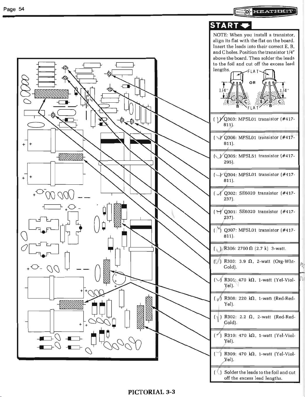
Page
54
START•
NOTE:
When
align
its flat
with
the
Insert
and
above
to
lengths .
leads i
C holes. Position
the
board.
the
foil
and
you install a transistor,
the
flat
on
the
board.
nto
their correct
the
Then
cut
off
FLA
TIE]}
transistor 1/4"
solder
the
E,
B,
the
leads
excess lead
+ +
i
8 ).
295).
Q302: SE6020 transis tor (#417-
237).
Q301: SE6020 transistor
37).
Q307: MPSL01 transistor (#417-
811).
~~:~
:i
: MPSL01 transistor
: MPSL01 transistor (#417-
: MPSL51 transistor (#417-
3-watt.
(Org-Wht-
2-watt
(#417
(#417
-
-
PICTORIAL 3-3
R308: 220
Yel).
2.2
R310: 470
Yel).
Solder
the
off
leads to
the
excess lead lengths.
kfl,
1-watt (Red-Red-
n, 2-watt (Red-Red-
kfl
, 1-watt (Yel-Viol-
the
foil
and
cut
Page 57

Page 55
C312: 1 pF
Wht).
"
l,V'
C317: 3.3 pF ceramic.
(..t C319: .0033
NOTE
: When
capacitor, match
or
color
positive ( +)
dot
C311
: 1.5
) C310: 1.5
) C314: 500
] C315: 500 pF ceramic.
) Solder
off the excess
you
on
mark
!LF
ILF
the
phenolic
JLF
install a
the
the
capacitor
on
tantalum
tantalum
pF
ceramic.
leads
lead
cer
amic
positive
the
circuit board .
.
.
to
the foil
lengths
(Brn-Blk-
.
tantalum
(+)mark
with
the
and
cut
.
PICTORIAL 3-4
Page 58

Page
56
NOTE:
When
tic capacitor,
mark
on
+)
mark
C305: 1200
C307: 1200
C303: .1
the
on
When
, match
with
(
NOTE:
capacitor
capacitor
PULL~END
ROUGH
SIDE~
t
CABLE
TIE-/
CATCH
~
&SS
ff.._.CUT
'i?V=
you install
match
capacitor
the
circuit board.
JLF
electrolytic.
JLF
electrolytic.
you install a
the
the
band
JLF
paper.
CIRCUIT
Detail 3-5A
an
electroly-
the
positive (
with
the
band
on
the
positive
paper
on
the
circuit
BOARD
+]
OFF
C302: .1
C301:
C320: 25
the
capacitor
mark
negative
capacitor
mark
( \1 ) C306: 1200
C304: 1200
Solder
off the excess
Refer to Detail3-5A
six cable ties
board holes
and
capacitors. Be
of
capacitor. Fit
through
cable
excess cable tie.
JL
.1
JLF
positive (
on
the
on
the
the
tubular
the
cable tie is
the
tie
F
paper
.
paper.
JLF
electrolytic. Match
+)
the
board
(-)
mark
the
board.
JLF
electrolytic.
JLF
electrolytic.
to
lead
through
and
around
sure
the
catch
Then
mark
positive (
or
match
negative
the
foil
lengths
and
the
electrolytic
the
rough
toward
cable tie
and
cut
with
with
leads
tight.
on
on
and
.
install
circuit
the
paper
pull
off
the
+)
the
the
(-)
cut
the
side
the
end
the
the
PICTORIAL 3-5
Page 59

Page
57
~~EI;IIIIII;I~~~~~---------------------------------------------------------------
-c::::::J
-c:::::::J
~G
o=S'~
~
-{lm~
~a
Refer
to Pictorial 3-6 for
-c:::J
L:::J-
6
oo
or'-----------',1
the
-c=:J-
_l_
:
POWER
CIRCUIT
following steps.
SUPPLY
BOARD
+
I+
PICTORIAL 3-6
I
HEAT
SINK
I
(I U303:
(#442-618)
board.
mark
in
their
the
IC
its
pins
(
r./
Refer
location U303
sure to
rial 3-6.
/'
Now
i
off
the
[
~
)
U301:
(#442-617)
Position
(
YJ
U302:
(#442-617)
Position
RefertoDetail3-6A
at
location
Match
on
tight
to
solder
In
the
the
circuit
holes
in
against
at
this
time.
Detail 3-6A
with
position
excess
the
In
the
the
the
pins
pin
the
same
and a heat
heat
the
same
and a heat
heat
notch
board
the
circuit
the
and
3-48 x 1/4"
heat
ofthe
lengths.
manner,
sink
manner,
sink
and
install a UA79IC
U303
in
board
sink
sink
as
sink
as
on
the
IC
and
insert
board.
but
mount a heat
as
shown
IC
to
the
install
at
location
shown.
install
at
location
shown.
the
with
the
the
IC
Then
do
not
sink
hardware.
in
foil
and
a UA78
a U78 IC
circuit
index
pins
press
solder
at
Be
Picto-
cut
IC
U301.
U302.
Detail 3-6A
Page 60

Page
58
CIRCUIT BOARD CHECKOUT
Carefully
inspect
the
circuit
board
conditions.
Unsoldered
solder
Poor
Solder
Protruding
Transistors for
connections
connections.
bridges
leads
between
which
proper
.
the
could
type
for
the
following
foil patterns.
touch
together.
and
installation
( ) Electrolytic capacitors for
the
of
positive (
( ) Diodes for
tion
of
the
( ) IC's for
There
board
are a
which
proper
number
will
+)
the
proper
banded
type
of
be
used
end
end
unused
.
type
.
and
installation
later.
the
correct position
and
the
correct posi-
holes
in
the
Set
the
circuit
.
circuit
board
aside temporarily.
.
Page 61

[[!
~
'if*ifih*ii
CHASSIS
Open
the
pack
marked
remaining
ing list.
bers
(Illustration Booklet,
on
The
the
parts
key
Chassis
in
the
numbers
and
#4
and
check
final
pack
corresponding
Final
Pack
Pages 9 and
these
against
the
to
Parts Pictorial
10).
PARTS LIST
and
follow-
the
the
num-
To
order a replacement
inside
"
Heath
the
rear cover. For
Parts
Price
part
List."
, see
"Replacement
prices
, refer to
the
Page
59
Parts"
separate
KEY
HEATH QTY. DESCRIPTION CIRCUIT
No
. Part
CIRCUIT
A1
A1
A2
A3
A4
AS
AS
A6
A7
AB
A9
A10
A11
A12
No.
COMPONENTS
6-473
6-104
1-31-1
5-2-3
3-12-10 1 500
10-1118
10-1119
25-228
54-953
60-2
60-4
60-54
60-73
60-624
411-815
47 k.n, 1 /2-watt
(Yei-Vioi-Org) resistor
100
(8rn-81k-Yel) resistor
330 k.n ,1-watt,10%
(Org-Org-Yel) resistor
270
3 1 000 n ( 1
1
1 00-1 00-300
electrolytic capacitor
Power transformer
1
DPDT 2-position slide switch
2 SPOT 2-position slide switch
DPDT 120V-240V
slide switch
DP3T 3-position slide switch
DP4T 4-position slide switch
5DEP31 F cathode ray
tube (CRT)
k.n
, 1 /2-watt
n,
3-watt, 1 0% resistor
n,
1 0-watt, 1 0% resistor
k)
control
M!l
control
ILF
Comp. No.
R13
R16
R17
R15
R14
AS
, R7, R8
R6
C3 A, 8 ,C,
T1
SW9
sw7,
SW8
SW10
SW6
SW4
V1
KEY HEATH
Part
No.
QTY. DESCRIPTION CIRCUIT
No.
Comp.
Circuit Components (Cont'd.)
412-15 NE2H pilot lamp
.•
A13
A14 421-20
1 /2-ampere, 3AG,
slow-blow fuse
PL1
F1
HARDWARE
NOTE: The hardware may be packed
velope (stamped HDW). Open all the hardware envelopes
according to size before you check the hardware against the
Parts List.
#4
Hardware
81
250-375 2
82
252-15 2
83
254-9 2
4-40 x 5 /16" flat head screw
4-40 nut
#4
lockwasher
in
more than one
en-
No.
Page 62

Page 60
KEY HEATH QTY. DESCRIPTION
No.
Part No. Comp. No.
#6
Hardware
250-1282
C1
C2 250-1164 6
250-138
C3
250-365 2
C4
250-1157 12
C5
250-32
C6
250-89 12
C7
250-1101 1
C8
250-591
C9
C10 250-1203
250-29 2
C1
1
252-3 25
C12
252-22 2
C13
254-1 26
C14
255-63 3
C15
259-1 3
C16
#8
Hardware
250-1138 8
01
254-4 4 8-32 nut
02
252-68 8
03
254-2 4
04
6-32 x 1/8" black setscrew
9
6-32 x 3
6-32 x
17
#6
washer head screw
6-32 x 1/4" hex stud
6-32 x
2
6-32 x 3/
6-32 x 3/8" T-bolt
#6
5
#6 x 9/16
1
6-32 x 3/4" screw
6-32 nut
6-32 push-on nut
#6
6-32 x
#6
/1
6" flat head screw
3/16" screw
x 1/
4"
hex F4 204-2314
3/8
" flat head screw
8"
screw
x 1/2" screw
" screw
lockwasher
2"
threaded spacer
solder lug
#8
x 5/
8"
hex washer
head screw
8-32 push-on nut
#8
lockwasher
Other Hardware
10-32
252-5 2
E1
254-37 2
E2
252-73
E3
E4 252-7 5
253-10 7
E5
E6 254-4
4
nut
#10
lockwasher
5/16" push-on nut
3/8" nut
3/8" flat washer
3/8" lockwasher
LINE CORD - HARNESS - CABLE
89-54
134-237 Cable with connector
134-1021 Harness
Line cord
CIRCUIT KEY HEATH
No. Part No. Comp.
METAL PARTS
F1
200-1348
204-2141
F2
204-2313 2
F3
F5 206-1216
206-1274 1
F6
207-1 2
F7
MISCELLANEOUS
G1
73-5
G2 73-34 2
73-45 7 Plastic grommet
G3
75-52
G4
75-754
G5
75-771 4
G6
92-609
G7 92-679
211-49 Handle
260-16 2
G8
261-1 3 Foot
G9
266-991
G10
~
00-18
351-9
G11
354-5
413-10
G12
414-36
G13
422-1 Fuse block
G14
G15 431-82
G16 434-41
436-11 3 Red socket
G17
436-22 1
G17
462-1049 2
G18
G19 462-1055
462-1059 4
G20
490-14
G21
205-778
G22
QTY. DESCRIPTION
Chassis
1 Front panel bracket
CRT bracket
Circuit board bracket
CRT shield
Input shield
CRT clamp
3/4" x 5" rubber strip
Red
alligator clip insulator
Slide switch insulator
Line cord strain relief
Slide switch cover
Cabinet shell
Cabinet front
Alligator clip
4 Plastic spacer
Felt strip
1
Epoxy glue packet
2 Cable tie
Red lens
Graticule
Terminal collar
1 CRT socket
Black socket
Red knob
2 Large black knob
Small black knob with skirt
Allen wrench
Alignment tool blade
(2-1/2'1
CIRCUIT
No
J3, J4, J6
J5
.
Page 63
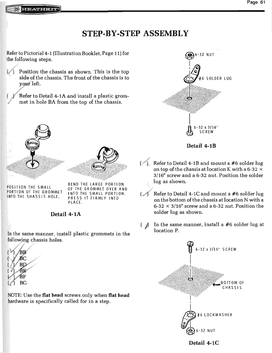
STEP-BY-STEP ASSEMBLY
Refer
to Pictorial4-1 (Illustration Booklet, Page 11) for
steps
the following
)
Position
side
of
ymn
left.
(
/
)
~
fer
to
met
in
.
the
chassis as
the
chassis.
Detail4-1A
hole
BA from
shown.
The
front of
and
install a plastic
the
top
of
This
the
the
chassis
is
the
is
grom-
chassis.
top
to
ft
6-32 X
@
Detail 4-1B
3/16"
SCREW
Page
61
POSITION
PORTION
INTO
In
following chassis holes.
(
~
the
THE
same
THE
SMALL
OF
THE
SHASSIS
manner,
GROMMET
HOLE.
Detail 4-1A
install
c /
B/
NOTE:
hardware is specifically
Use
the
flat head
BEND
THE
LARGE
OF
THE
INTO
PRESS IT FIRMLY INTO
PLACE.
screws
called
GROMMET
THE
plastic
only
for
SMALL PORTION .
in
PORTION
OVER
grommets
when
a step .
AND
in
the
flat head
( ~ Refer to Detail 4-1B
on
top
of
the
chassis
3/16"
screw
and
a 6-32 nut.
lug
as
(/ Refer
on
the
6-32 x 3/16"
solder
In
the
location
shown
to
bottom
same
.
Detail4-1C
of
screw
lug
as shown.
manner,
P.
'f
the
6-32
I
,
c;o!f:i\iffl,lflf~
I
and
mount a #6
at
location K with
Position
and
mount a #6
chassis
and
at
location N with
a 6-32 nut.
install a #6
X 3/16"
SCREW
!':,o
solder
lug
a 6-32 x
the
solder
solder
Position
solder
:;~~~
~F
lug
lug
a
the
at
Detail 4-1C
Page 64

Page
62
( ) Refer
1/4"
location
nut.
In
the
same
studs
at
(
CB
cc
( /)
( I
CD
CE
C
;Jl
CF
CG
~
~
( )
CH
( )
CJ
( )
CK
)
(
CL
( )
CM
to
hex
This
manner,
the
following
Detail4-1D
stud
on
the
CA
with a #6
stud
will
loosely
chassis
@ 6-32
~#6
and
loosely
bottom
lockwasher
be
tightened
mount
holes
NUT
LOCKWASHER
mount
of
6-32 x 1/4"
.
the
and
later.
a 6-3 2 x
chassis
at
a 6-32
hex
K Refer
threaded
location
lockwasher.
Detail
to
Detail 4-1F
spacer
Q. Use a 6-32 x 3/8"
on
4-tE
the
and
bottom
install
of
screw
a 6-32 x
the
chassis at
and a #6
2"
(
vJ
Refer to
nut
in
of
the
use
the
(
In
the
v/ locations
( / ) Install
the
flat
chassis.
Detail4-1D
Detail4-1E
the
slot
nut
is
on
two
6-32
same
manner,
J,
L,
an
8-32
side
of
tlh
6-32 X
llJI
HEX
at
location
the
bottom
push-on
and
M.
push-on
the
nut
1/4"
STUD
and
install
H. Be
of
the
nuts
install8-32
nut
at
on
the
rear
an
8-32
push-on
sure
the
flat
side
chassis. Do
at
this
push-on
location T with
(outside) of
not
time.
nuts
the
at
In
the
spacers
same
manner,
at
locations
"
'
~iiH~,~-~~~i~~;
install6-32 x 2"
Rand
. f 6-32 x 3/8"
threaded
S .
SCREW
~:;~~I
~f
J';~LOCKWASHER
6-32 X 2"
SPACER
( · )
In
locations U, X,
the
same
manner,
andY
install8-32
on
the
rear
push-on
of
the
nuts
at
chassis.
Detail4-1F
Page 65

Page
63
~
10:
Refer
120V-240V
chassis
screws. Be
lugs
the
at
with
the
front of
to
Detail4-1G
slide
switch
location
sure
the
bare
wire
the
chassis.
SW10
switch
between
~
6- 32 X 3/16"
and
on
is
the
with
~
mount
positioned
the
bottom
6-32 X 3/16"
them
is
DPDT
of
the
so
the
toward
Detail4-1H
BARE
WIRE
Detail4-1G
Refer
to
Detail 4-1H
on
the
bottom
; -32 x 3/8" hardware.
( ..{ Refer
;h
(
.!]'
; bracket
to
ray tube)
either
In
of
ardware.
the
of
Detail4-1J
bracket
the
V1
same
manner,
at
the
I
Install a 6-32
CRT
f
nut
shown
bracket. Be
is
up
on
push-on
and
Pictorial 4-1.
and
mount
the
chassis
and
mount
on
the
top
locations. Use 6-32 x 3/8"
install
remaining
sure
that
nut
that
each
V1
nut
the
at
location
a CRT (cathode
of
the
the
other
location
on
the
top
the
flat
side
is
positioned
fuse
chassis
.
block
F1
of
of
with
at
CRT
each
each
as
@ @
~/
~@#6
0
® ®
Detail
4-lJ
6-32
~
\\
n
6-32
I
CRT
SCREW
BRACKET I
NUT
LOCKWASHER
x 3/8"
Page 66

Page
64
Detail
4-lK
Detail
( ) C3: Refer to Detail 4-1K
JLF
100-300
the
top
inset
positions
( ) T1 : Refer to Detail 4-11
transformer ( #54-953)
lockwashers
the
transformer so
located
RefertoP"1orial4-2 (Illustration Booklet, Page 12) for
the f owing
Refer
lens
in
push-on
positioned
tight
(v }/pLl:
Push
pilot
electrolytic capacitor (#25-228) on
of
the
chassis at
drawing
as
to
hole PL1
against
lamp
which
from
the
and
shown.
steps.
Detail 4-2A
nut. Be
as
shown
the
the
pilot
lens.
4-lL
and
location
shows
bottom
8-32 nuts. Be
the
in
sure
chassis.
of
and
at
location
proper
and
install
the
chassis
the
slot
before you
lamp
all
mount
C3. Refer to the
the
the
mount
sure
color wires are
the
the
capacitor lug
chassis.
the
power
T1
with
to
position
the
pilot
with
a 5/16"
in
the
lens
push
the
way
into
100-
#8
lamp
nut
the
is
Refer to Detail 4-2A
lar
onto
the
pilot
lamp
even
with
the
end
minal
collar so its
and
push
lens
of
the
lens.
lugs
are located as
the
terminal
until
the
Position
col-
collar is
the
ter-
shown.
Page 67

Detail 4-2A
efer
to
the
install a
cal circuit
side
chassis.
of
split
the
Detail 4-2C
inset
drawing
bearing (furnished
board
parts)
in
bearing
must
be
on
Pictorial 4-2
with
hole
R4A.
on
the
the
The
inside
Page
and
verti-
wide
of
65
the
#4
Detail 4-2B
((.)""' SW4: Refer to Detail4-2B
4-position
4-40 x 5/16" flat head
be
mounted
~
SW6
3-position
6-32 X 3/16" flat head screws.
(
v{
SW7:
2-position
tion
slide
either
'
Refe,
to
slide
In
the
slide
the
switch
switch
Detail
switch
same
switch
so its
hard
way.
4~2C
manner,
lugs
(
~
Refer to Pictorial4-3 (Illustration Booklet, Page 13) for
the
the
hole
R4B
follcSwing
same
steps.
l
T
urn
the
LOCKWA~
4-
40
NUT~
and
mount
at
location
ware. The
and
at
location
install
at
location
are
located
the
SW4
switch
imtall
SW6
an
SW7 . Posi-
as
DP4T
with
can
a DP3T
with
SPDT
shown
.
Locate
with
as
...r-i'ass
(
for
) Pass
for
p Pass
small Gry-Wht wires from
grommet
transformer T1. Pass
ness
later.
the
the
shown
the
wires from
connection
the
wires from BO#B
connection
the
large Brn, large Red, large Org,
wist
together
and
manner,
.
chassis over
harness
wires from
.
BE
through
and
B0#1
later.
later.
for
connection
the
two
grommet
install a split
and
position
position
the
various
through
through
B0#9
later.
green
leads
these
leads
BE
bearing
it
as
shown.
it
on
the
breakouts
grommet
grommet
and
through
coming
under
the
for
connection
in
chassis
(BO)
BA
BF
the
from
har-
·
SWB:
In
the
2-position
same
slide
manner,
switch
install
at
location
another
SWB
SPDT
.
Page 68

Page 66
Refer
to
Pictorial4-4
the
following steps.
(Illustration Booklet, Page 14) for
Refer
the
following
to
Pictorial4-5
(Illustration Booklet, Page 14) for
steps.
Connect
SW10 as follows. Make
tions. (See
{J
) Blk-Grn
(
./
! )
(A Blk-Red
Connect
a;ollows.
(})
)}
~
Connect
as follows:
the
leads
the
inset
lead
Blk
lead
to
lug
Blk-Yellead
lead
the
wires
coming
Make
mechanically
Either
largeBrn
OtherlargeBrn
Connect a 1"
tion
from a
capacitor
the
C3
wires
coming
from
drawing
to
6 (NS).
to
to
wire
wire
bare
1"
lug
transformer
mechanically
on
lug
5 (S-1).
lug
2 (S-1).
lug
3 (NS).
from
B0#7
secure
to
fuse
to
switch
wire
(remove all
length
4 (S-1)
from
of
to
B0#9
T1
to
secure
Pictorial 4-4.
blockF1lug
SW10
brown
solder
connec-
in
the
connections.
lug
the
wire) from
lug
N (NS).
in
the
switch
harness
2 (S-1).
3 (S-2).
insula-
harness
( } Locate
.f/
tion
Connect
to
the
(
LY
Wht-Grn
/
( l/) ,
Wht
(
11
Grn
( Vl Viol
(/) / Wht-Gry
Connect
to
the
(
()
Either Gry
/
(//
Other
it
the
power
w1re to
wire
wire
the
power
the
as
wires
.
wires
Gry
power
shown.
coming
supply
wire
hole
to
hole
to
hole
to
holeY
coming
supply
wire
wire
supply
circuit
to
holeS
R (S-1).
AA (S-1).
AD (S-1).
(S-1).
circuit
to
hole
to
hole
circuit
from
board
from
board
Q (S-1).
V (S-1).
B0#3
as follows :
(S-1).
B0#4
as follows:
board
of
the
of
the
and
posi-
harness
harness
( ) All five Blk
all wires,
dered.
(
IY'
Both Viol
( · Both Wht-Red
/
( V) Red
~
(
(_ .
.Y
~
(Y R-15:
wire
Place
500
n'
R14:
tween
resistor
la
~ e
270
n'
tween
resistor
wires
especially
wires
to
capacitor
a
1"
length
10-watt resistor.
Connect
lugs
1 (S-3)
directly
a 5/8"
length
3-watt resistor.
Connect
lugs
2 (S-4)
1/2" above
to
to
capacitor
wires
of
this
resistor
above
of sleeving
this
resistor
the
solder
to
sleeving
and
and
lug
the
lower
capacitor
C3
lug
to
2 (NS).
the
capacitor
3 (S-2).
chassis.
N (S-6). Be
ones, get sol-
C3
lug
C3
3 (NS).
on
each
capacitor
Position
on
each
to
capacitor
Position
1 (NS).
lug
2 (NS).
lead
C3
lugs.
lead
C3
sure
of a
be-
this
of a
be-
this
(
C(
Any
( ' Either
Remaining
(\ )
Connect
to
(
1.
( )
( K
the
power
Blk
Either
Other
Wht-Red
Wht-Yel
Wht-Brn
the
wire
of
the
ofthe
wires
supply
Org
Org
three
remaining
Yel
coming
to
holeD
wire
wire
wire
wire
to
wire
to
Yel
wire
circuit
(S-1).
to
hole
to
hole
to
hole
hole
hole
wires
Yel
to
hole
from
board
P (S-1).
U (S-1).
J (S-1).
L (S-1).
K (S-1).
to
hole
wires
to
AH (S-1).
B0#5
of
as follows:
N (S-1).
hole
T (S-1).
the
harness
iliijiiii)
Q .5 1
I I I
(CM)
(INCHES)
2
3
2
. I ' I ' I '
I'
I I
3
' I ' I • I '
I I I I
8 9
I I
I
10
4
I I I
I I I
11
12
13
I I
1.
1"
I I I
17
7
I
Page 69

Page
67
~
6-
\
32 X 3
H
POWER
CIRCUIT
/16
"
~
SUPPLY
BOARD
f
'T
<ID
~~~~--------~
J
~
@
()
PICTORIAL 4-6
@
f)
[01,
~
I
\QJ
()
0
~
'
Connect
to
Refer to Pictorial 4-6 for
Connect
the
(y Large
( ) Either large
(
~
the
wires
coming
the
power
Large Blk
Large Org
Large Red
Large Yel
po
Other
supply
the
leads
er
supply
Wht-Yellead
large
circuit
wire
wire
wire
wire
coming
circuit
Yellead
Yellead
to
to
to
to
hole
hole
from
board
hole
hole
the
from
board
to
to
to
B0#6
as follows:
AE (S-1).
X (S-1).
W (S-1).
AF (S-1).
following
the
transformer
as follows:
hole
AB
hole
E (S-1).
hole
C (S-1).
of
the
steps
(S-1).
harness
.
T1 to
~
arge
(
(V ) Large
(~Either
/.
(
(~Either
/o
(
This
complete
board. Be
off all excess
ble.
Wht-Brn
Wht
large Red
Other
large Red
large Brn
ther
large
l-L/
/
S'me
sure
lead
~
Temporarily
board
at hex
screws.
lead
to
lead to hole H (S-1).
lead
lead
to
lead
to
Brn
lead
to
-z.c
~
wiring
all
connections
lengths
studs
mount
CL
to
as close
the
and
hole
I (S-1).
to
hole
F (S-1).
hole
G (S-1).
hole
A (S-1) .
hole
B (S-1).
the
po~er
are
soldered, and
to
power
CH
with
supply
the
foil as possi-
supply
6-32 x 3/16"
circuit
cut
circuit
Page 70

Page
68
SHIELD
TAKING
REMOVE
CARE
THE
OUTER
REMOVE
NOT
~
REMOVE
INSULATION
I
NNE R LEA
THE
FOIL
FROM
D. Detail
LEAD
TO
CUT
THE
INSULATION.
SHIELD LEAD,
INNER
LEAD
~
/')'~s~1~~D
AND
THE
V"
REMOVE
END
4_7
OF
A
1/4"
THE
LEAD
OF
DO NOT
this
cable;
~
(
/
)/f
~onnect
the
will
Connect
the
will
Position
( )
as
Connect
to
the
~
)
Blk
(
(
I)
Viol
( / ) Yel
remove
it
repare
will
the
any
insulation
be
connected
ends
of
an
8"
e.
one
end
of
an
8"
vertical
be
vertical circuit
be
shown
the
vertical circuit
wire
wire
wire
circuit
connected
one
end
connected
the
vertical
in
Pictorial 4-7.
wires
coming from
to
hole
to
hole
to
hole
board
later.
of
an
board
later.
circuit
board
(
~)
N (S-1).
W (S-1).
8"
as follows :
from
later.
Gry
wire
Gry
wire
(S-1).
Blu
wire
(S-1).
board
B0#10
ground
the
and
in
The
in
The
on
of
(S-1).
free
an
hole
other
hole
other
the
the
end
of
8"
Blu
Y2
in
end
Y1
in
end
chassis
harness
Refer
to
Pictorial4-7 (Illustration Booklet, Page 15) for
the
following steps.
( 6 Refer
20"length
vertical
Connect
lead
~
(
~
Connect
lead
the
to
the
Inner
Shield
At
the
insulation
to
identify
Refer
length
26"
the
to
the
to
Detail4-7 A and
of
shielded
circuit
end
vertical
lead
lead
other
to
Detail4-7 A and
end
vertical
of
this
circuit
to
hole
to
end
from
this
of
shielded
of
circuit
board
hole
the
cable
this
prepare
cable
parts).
cable
board
HH (S-1).
KK
(S-1).
of
this
inner
lead.
when
prepare
cable.
cable
board
(furnished
with
the
as follows:
cable,
remove
This
it
is
connected
with
the
as follows:
both
bared
will
both
bared
ends
with
1/4" of
be
later.
ends
of a
the
inner
used
of a
inner
( / ( Org
(!) Gry
( o{/ Wht-Grn
( v[
This
board. Check
and
possible.
Refer to
the
wire
wire
Grn
wire
completes
cut
off all excess
Pictorial4-8
following steps.
~
Secure
with
through
holes
the
CD,
hex studs.
the
two
Band C and
circuit
CE,
to
hole
to
hole V (S-1).
wire
to
to
holeD
the
to
see
that
lead
vertical
#6
x 1/4"
the
switch
board
and
CF.
U (S-1).
hole
C (S-1).
(S-1).
wmng
(Illustration Booklet, Page 16) for
and
Then
of
the
vertical
all
connections
lengths
circuit
6-32 X 3/16" screws
into
as close
board
hex
washer
bracket
hex
tighten
are soldered,
to
to
the
head
and
into
studs
CA, CB, CC,
the
nuts
circuit
~he
foil as
chassis
screws
chassis
through
on
the
lf
)
Inner
)S
hield
lead
lead
in
hole
in
hole
H (S-1).
K (S-1).
Page 71

Detail 4-9A
Page
69
. /
~
~
/ r
/ Pass
NOTE:
on
the
free
=~:!~g
the
connection
ass
the
the
for
from
harness
the free
vertical
connection
the
free
vertical
connection
Position
the
and
later.
end
circuit
end
circuit
the
harness
later.
later.
gJ wires.
Position
( )
power
the
stall a cable
inset
tight
the
transformer T1
corner
of
the
tie
drawing
and
on
cut
off its excess.
indicated
around
ends
of
the
two
shielded
vertical
then
of the Blu
board
of
board
through
through
the
Gry
through
away
circuit
grommet
wire
wire
from
leads
on
top
of
the
vertical
circuit
all
these
Pictorial4-8. Pull
cables
board
under
BF for
coming &om
grommet
coming
from
grommet
these
blue
coming
harness
board
from
near
and
wires. See
the
cable
BC
BD
and
in-
the
tie
Remove
DANGER label
the
power
Set
the
chassis aside temporarily.
Refer to
the
Pictorial4-9
following steps.
the
chassis at
supply
protective
and
press
the
location
circuit
(Illustration Booklet, Page
CAUTION: Place a large soft
the
'to protect
you
work
SW9: Refer to
2-position
cabinet
Set
the
cabinet front from
with
the
Oscilloscope.
Detail4-9A
slide
switch
front. Use 6-32 x 3/8" flat head screws .
cabinet
front aside temporarily.
board
cloth
at
backing
the
label
shown
.
12/S""
on
your
being
and
mount
location
from
in
place
near
17}
work
area
scratched
the
DPDT
SW9
on
the
on
the
for
as
the
0
11{e
rilijiiil)
0
..
~
I
a~e
1
"!.
%
7 / 8
~:e
I
I
I
I
I
1
(CM)
2
(INCHES)
I
I
I I
I
I
I
3
I
I
2
I I
I I
I
I
I
•
"
3
I
I I
I
I
I I
I
•
I
I
I
I
"
4
I I I I I I
I
10
I
I
,
5
I
I
12 13
6
.
I
I
I
I
I
1.
I I I
I I I I I I I I
I
I I
1<5
"'
I
I
I
7
I
17
Page 72

1-'age
70
FRONT
PANEL
0
0
()
0
FROM
l
DO
REMOVE
0
I
-1
f--l/4
" f
l -
3/8"
:.a__L.~V~II
l/4"....
,.......,__
0
5"
~
D
PROTECTIVE BACKING
oD
~o_o~lo
__
o~--~--~
I
BOTTOM
EDGE
NOT
THESE
AREAS
0
1/4"-l
\
~if
¥
~1
:.~~
o
:
~:..:
0 o
0§0
~
W
---~o~
1
~.
L
l/4
"
0
NOTE:
remove
printed)
ing
otherwise,
recessed areas of
adhesive
five
tive backing
sharp
backing,
on
(
In
the
the
protective
side
of
must
not
be
the
back
switches
knife.
the
~
Refer to Detail 4-9B
backing from
for
vious note.
Temporarily
up
from operating.
around
Then,
be
sure
front panel.
the
two
on
your
next
switch
of
step,
the
front
removed
covers,
the
cabinet
the
front
these
when
these
shaded
the
back
shaded
lay
the
work
you
backing
panel.
from
front,
panel,
Cut
two
you
remove
and
of
areas
front
area.
will
be
instructed
from
the
The
protective back-
the
two
shaded
positioned
will
and
prevent
through
shaded
the
areas
remain
remove
the
mentioned
front
panel
the
adhesive
back
in
the
stick to
the
protec
areas
with
protective
in
protective
panel
except
in
the
Detail 4-9B
to
(un-
areas;
five
the
these
-
a
place
pre-
side
( Fit
1
(
~
Locate
metal)
Install
location
((-~
( 1)
( /
NOTE: Be
their
the
6-32 x 3/8" T-bolt
square
Place
recessed areas at
SW7,
1.
2.
3.
recessed
recess
a 2-1/2"
and
SW8
the
three
slide
supplied
these
SW3
1-7/16"
1-3/16" metal
down
29/32"
covers
sure
with
in
the
switch
into
switch
the
areas
in
slide
the
switch
into
the
cabinet
switch
switch
in
the
switch
the
vertical
in
the
following order.
cover.
switch
cutout
cover.
covers
when
you
front.
cover
locations SW4, SW6,
cabinet
covers (two fiber
circuit
recessed area
cover. Be
in
the
and
perform
the
indicated
in
each
of
front.
and
board
parts.
at
switch
sure
its tabs fit
1-7/16" cover.
T -bolt
remain
the
next
step.
the
one
in
( )
0
',4
I 1 ! 8 I
''"''''')
5
0
Position
4-9.
%
3~8
I
1
the cabinet
o/.
7/8
5(a I
(CM
I I I I
I
I
I
I
) 2 3 5 e 8
I
I
(INCHES
I
front as
) 2
I
I
I
shown
I
I
I
I I
I
in
Pictorial
3
I
I
I
I
I
I
(J
I
I I
I
9
Carefully fit
down)
front. Press
4
I
I
10
into
I I
I
I
I
I
11
the
front
the
recessed area of
the
front
5 6
I
I
I
I
I
I
12
13
panel
I
I
I
panel
I
.
I
1~
down
I
I
I
I
15
(adhesive
the
cabinet
into
place.
I I
I I
I
"'
side
I
I
17
7
I
Page 73

= :
jcHASSisl
Page
71
(
~
(
(
(
Refer
( )
NOTE:
line
cabinet front
~
:
Install a
panel. Use
/
~
4:
In
the
location J4.
.(
J5:
Install a black socket
.J
J6:
Install
J6.
to Pictorial 4-10 for
Temporarily
switches
If
necessary,
up
with
the
in
it
the
cabinet
Be
sure
erly
into
red
socket
the
nut
same
the
remaining
.J_U-/s-
10'5:>C>--
remove
SW2A
slide
slide
the
following
front
all
the
switches
their
slots
at
furnished
manner,
the
the
and
SW2B.
the
switches
onto
and
location
install a red
at
red
following
3/8-32
switch
when
steps
the
and
holes.
J3
with
location
socket at
nuts
covers so
you
.
front of
the
T -bolt fit
PICTORIAL
in
the
front
the
socket.
socket
J5.
location
steps
.
from rotary
they
mount
the
the
chassis.
prop-
at
4-10
Install 3/8" flat
tary
switches
Install a
T-bolt
( )
R8:
location
washer,
so its
l'
\l R7: In
control (#10-1118)
( )
R6
tion
control so it does
chassis.
R5: Install a 1000 0 (1k) control ( #10-1118) at
location
at
Mount
and
lugs
the
: Install a 1
R6. Cut
washers
SW2A
#6
lockwasher
hole A
R8
R5.
in
a 1000
with
a 3/8"-32 nut.
are
located
same
manner,
MO
the
and
3/8-32
and
SW2B.
and
a 6-32
the
chassis
0(1k)
a 3/8" lockwasher, 3/8" flat
as
at
location
control (#10-1119)
control locating tab off
not
touch
front.
control (#10-1118)
Position
shown
install
.
a 1000 n (1k)
R7.
the
nuts
nut
the
inside
on
ro-
on
the
at
control
at
loca-
the
of
the
Page 74

Page
72
Refer
to
Pictorial4-11
the
for
~
Connect
as
following
)
Position
Push
switch
the
follows:
Either
the
SW9
wires
large
Make a mechanically
Other
large
Make a mechanically
( '-)
Wht-Brn
(
tJ_.,.--
Blk
wire
ass
the
through
steps
the
chassis
slide
switch
.
coming
Brn
wire
Brn
wire
wire
to
to
socket
Wht-Red
grommet
(Illustration
.
upside
insulator
from
B0#2
to
switch
secure
to
switch
secure
socket
J5
BB
J3
(NS).
wire
for
(S-1).
coming
connection
Booklet,
down
as
shown.
onto
the
of
the
SW9lug
connection
SW9lug
connection.
from
later.
Page
17)
rear
harness
6 (S-1).
.
5 (S-1).
B0#2
Gril
to
1
I
Blk
(
Wht
solder
lead
lead
to
to
lug
fuse
switch
P (S-1).
block
SW10
F1
lug
of
ALTERNATE LINE VOLTAGE OPERATION
This
Oscilloscope
or 240 VAC
is
most
more
is
THAT
AREA.
120
VAC LINE VOLTAGE
~
line
often
common.
AGREE WITH THE LINE VOLTAGE IN YOUR
Move
120
is
screwdriver
can
be
operated
voltage.
used, while
In
the
in
United
other
USE ONLY THE INSTRUCTIONS
slide
switch
visible
blade
on
SW10,
the
to
move
top
1 (S-1).
lug
6 (S-2).
on
either
States
countries
if
necessary,
of
the
the
switch
120 V AC
120 VAG
240 V AC
switch.
so
the
Use a
slider.
==t'J
)
:::TJ.
)
T )
Refer
(
.!)'
/
(
~
Pass
the
connect
must
Prepare
a 5-1/2"
Connect
socket
J4
through
Connect
(S-2).
Pass
grommet
to
Pictorial
Refer
to
Detail4-12A
line
cord.
Refer
to
Detail4-12B
of
the
line
chassis.
Refer
to
Detail4-12B
the
line
strain
relief
screw
.
end
of
its
leads
be
mechanically
Wht-Blu
one
end
(S-1).
Pass
grommet
one
end
the
other
BB
for
4-12 for
cord
through
cord
strain
at
location W with a #6
the
line
as
follows.
wire
of a 5-1/2"
the
other
BA for
of a
connection
3"
Blk
end
of
connection
the
following
and
prepare
and
pass
hole
and
install
relief.
cord
through
All
secure.
and a 3"
Wht-Blu
end
wire
this
later.
the
Win
the
Install
grommet
three
Blk
wire.
wire
of
this
wire
later
.
to
socket
wire
through
steps.
the
end
of
prepared
the
rear
of
line
cord
the
line
cord
x 9/16"
BG
and
connections
to
J5
the
end
the
in
~
~
F1:
\
in
the
(
Remove
1
label
chassis
Write
[
~
line
Install
fuse
the
block
the
and
press
at
the
"1/2-ampere,
on
the
fuse label.
1/2-ampere,
protective
the
indicated
240 VAC LINE VOLTAGE
( ) Move
( ) F1:
( )
( )
slide
switch
240
is
visible
screwdriver
on
blade
Install a 1/4-ampere,
(not
supplied)
Remove
label
and
chassis
Write
line
on
at
"1/4-ampere,
the
in
the
protective
press
the
indicated
fuse label.
the
at
location
label
3AG,
SW10,
the
to
move
the
fuse
label
3AG,
3AG,
backing
onto
location.
top
of
3 AG,
block
backing
onto
location.
if
slow-blow
Ft.
from
the
bottom
Slow-blow"
necessary,
the
switch.
the
switch
slow
blow
at
location
from
the
bottom
Slow-blow"
fuse
the
fuse
of the
on
so
Use a
slider.
fuse
Ft.
the
fuse
of
on
the
the
the
the
''"''''')
0 .5 1
I I I
(CM)
2
(INCHES)
I I I I ',1
2
.
,I
'I I II
s "
II
I
3
I I I I I
I I I
8
4
I . I I I
1
r
r
9
10
I I I I I
r I r
,,
7
I I I
12
13
I I
1~
I,~
1&
I
17
Page 75

Page
73
PICTORIAL 4-12
Detail
4-12B
·.::.
_..:;)
Page 76

Page
74
r -'
Refer to
for
the
following steps.
Position
( )
Connect
lows:
'
~
'i---f-
~
(
( r Y/
(
vf
~
~
Large
Large
Yel
Grn
Wht-Yel
arge
lk
/_
( ) R17:
sistor
(S-2).
Place a 1/2"
Connect
(NS)
Connect
ing
( / Locate
met
inner
SW4lug
ti
Remove 1/4" of
the
BF.
~
(
SW4lug
tion
Connect
from
Pictorial4-13
the
the
wires
Yel
Brn
Blk
wire
to
wire
to
wire
to
wire
Connect
to
control
this
and
7 (S-1).
the
from
grommetBA
the
BF
with
lead.
8 (S-1).
, n
at
this
other
shielded
nnect
the
6 (S-1).
at
this
the
grommet
(Illustration Booklet, Page 18)
chassis
from
wire
wire
wire
control
control
control
top
B0#1
to
control R6
to
control
to control
R5
R5
R5
to
switch
side
up
of
the
lug
R6
lug 2 (S-1).
R6
lug
lug
3 (S-1).
lug
2 (S-1).
lug
1 (S-1).
SW4 lug 5 (S-1) .
a 330k!l, 1-watt (Org-Org-Yel) re-
R6
length
of
wire to
free
end
shielded
the
insulation
Connect
There
end
of
insulation
inner
There
end
of
free
end
BB
between
sleeving
switch
of
to
cable
the
the
cable
lead
the
to
solder
lugs
on a 1"
SW4
the
Wht-Blu
switchSW4lug
coming
removed
inner
is
no
shield
cable.
from
coming
of
this
is
no
shield
cable.
of
the
Blk
lug
as
shown.
harness
3 (NS).
1 (NS) .
1 (S-2)
bare
between
wire
from grom-
lead
lead
the
inner
from
cable
lead
wire
K (NS).
as fol-
...
and
wire
lugs
com-
3 (S-1).
from its
to
switch
connec-
lead
grommet
to
switch
connec-
coming
3
.
4
of
Connect
ing
from
(NS).
Prepare
wire.
(\
J
Connect
3 (S-1) to
Connect
lug
1 (NS)
Connect
(S-2).
( )
Connect
lug
2 (NS).
Be
sure
the
R13:
PL1
between
Refer
to
Pictorial4-14
for
the
following steps.
CAUTION:
ing steps,
were
Connect
horizontal
sition
bles
do
connected
the
circuit
the
following six wires
connected
Wht-Org
wire
Grn
(
Wht-Red to control
Wht-Gry to control
Red
wire
Wht-Yel to control
Remove
1")
from
end
of
to
switch
the
free
grommet
a 2-1/2"
a 2-1/2" Blk
solder
a 6-1/2" Blk
to
one
the
pilot
lamp
Connect
When
you
not
burn
earlier.
free
ends
board
to
switch
wire
to
control
to control
an
additional
the
free
this
wire
SW6
end
of
the
black
lug
solder
lead
other
leads
BB
of
lead
wire
the
to
pilot
wire
from
K (NS) .
wire
from
lug
K (NS).
pilot
of
the
do
not
Wht-Red
and
lamp
pilot
touch
wire
lamp
PL 1 lug 3
a 6-1/2" black
switch
pilot
to
SW8lug
lamp
PL1lug
lamp
each
other.
a 47 k!l(Yel-Viol-Org) resistor
lugs
2 (S-2)
and
3 (S-2).
(Illustration Booklet, Page
connect
the
of
the
wires
insulation
the
wires
to
the
on
coming
chassis as follows. Po-
under
the
in
the
follow-
the
wires that
from the
shielded
SW4.
to control
end
through
lug
R8
R8
lug
R8
lug
R7
lug
R7
lug
R7
lug
3/4" of
of
the
switch
6 (S-1).
lug 3 (S-1).
2 (S-1).
1 (S-1).
3 (S-1).
2 (S-1).
1 (S-1).
insulation
Org wire. Pass
SW4lug
4 (S-3)
corn-
PL1
to
PL1
(total
1
to
19)
ca-
the
"'''"")
Q .
!5
I I I
1 (CM ) 2
(
INCHE.S
I
I' I Ill
)
. I . I • I I I I I .
I I I I I I I
e 1 e 9
3
I I
I
10
4
I I I 1 I
11 1'2
13 14
I I
I
15
6
·II
7
I
17
Page 77

Page 75
( ) Wht-Blu
Remove
(
\.2
3/4") from
Connect
through
Refer
to Pictorial 4-15 (Illustration Booklet,
for
the
following steps.
Connect
horizontal
l"
J Viol
(
~~
- ) Yel
(
1.-
c-r--
!
Refer
for
Connect
BF
( ) Yel
move
2")
17
Connect
(S-2)
Wht-Grn
) Wht-Brn
Wht
to
the following steps.
to
the
wire
to
an
additional
the
the
free
lug
7 (S-2)
the
free
ends
circuit
wire
from
to
wire
wire
Pictorial4-16
the
horizontal
wire
board
to
switch
an
additional1/4"
the
this
wire
lug
2 (S-1).
wire
to
to
switch
wire
to
to
switch
wires
from
to
hole W (S-1).
switch
free
end
of
free
switch
switch
(Illustration Booklet, Page 21)
circuit
end
of
to
the
to
the
SW6
end
to
switch
SW7
SW8
B0#8
SW6
1/2" of
of
this
lug
wires
chassis
lug
of
SW7
lug
SW7
lug
coming
board
lug 8 (S-1)
insulation
the
Wht-Viol
wire
to
1 (S-1).
coming
as follows:
4 (S-1) .
of
insulation
the
Wht-Blk
SW6
through
lug 3 (S
2 (S-1) .
lug
2 (S-1) .
from
as follows:
switch
Page
from
-1).
1 (S-1).
grommet
.
(total
wire
SW6
20)
the
(total
wire
lug
( ) Grn
Connect
cuit
.
This
board. Check
and
foil.
the
( ) Carefully
.
3
~
( ) Refer
I
(
wire
to
hole
the
following wires from
board
to
the
chassis as follows:
wire
to
Blk
Brn
wire
completes
then
cut
The
remaining
circuit
)
board
connected
shown.
Pass
the
chassis
a 3/8" flat
Refer
supply
CH.
mount
the
chassis
Remount
6-32 X 3/16" screws at
and
CL,
studs
solder
through
the
to
see
that
off all
the
will
position
to
shaft of
at
location
washer
to
Detail 4-16A
circuit
to
the
inset
the
circuit
with
the
power
CM.
Then
.
T (S-1).
the
horizontal
lug
K (S-4).
grommet
wiring
all
excess
Blu
and
be
connected
all
the
horizontal
the
SW5.
and
board
drawing
board
6-32 x 3/8" hardware.
tighten
BB
tosocketJ6
to
the
horizontal
connections
wire
lengths
Gry
wires
later.
the
wires
circuit
rotary
screws
supply
switch
Secure
a 3/8-32 nut.
and
remove
from
on
Pictorial4-16
bracket
circuit
hex
studs
the
nuts
the
at
CG,
cir-
(S-1).
circuit
are
soldered
close
to
the
connected
and
board
through
switch
the
holes
location Z on
board
CH,
on
to
harness
as
the
with
power
CL
and
and
with
CJ,
CK,
the
hex
r/(
(
( {
(
(
v{
,Y
Gry
org
~
ed
Blk
f
Wht
wire
wire
wire
wire
wire
to
to
to
to
to
hole
hole
hole
hole
holeS
V (S-1).
U (S-1).
X (S-1).
H (S-1).
(S-1).
( )
( )
Secure
board
3/8"
Position
horizontal
shown.
indicated
Pull
the
to
the
hardware
all
Then
the
cable
other
end
circuit
.
the
wires
circuit
install a cable
chassis
tie
holes
tight
of
board
connected
board
and
and
the
horizontal
bracket
and
Ue
around
cut
with
between
the
through
these
off its excess end.
circuit
6-32 X
chassis
the
wires.
the
as
two
Page 78

Page
76
INSIDE
CRT
SHIELD
OF
~
TAB
PICTORIAL 4-18
Refer to
for
Reposition
--L.J.
Pictorial4-17
the
following
Locate
sion
nished
Start
the
the
shafts,
with
two
coupling.
( ) Install a shaft
control R4B.
In
the
same
pling
on
It
NOTE:
may
control bracket
the
form
alignment
next
with
Pass a
priate
hole
coupling
5/16"
outside
setscrew
steps
chassis as
two
shaft
and
the
6-32 x 1/8"
coupling
Tighten
manner,
the
shaft of
be
necessary
mounting
two
steps) to get
the
front
5"
extension
in
the
on
control R4B so
the
in
the
(Illustration Booklet, Page 22)
.
shown.
couplings,
four
#6
vertical
the
install
control
to
hardware
panel
shaft
front
front
shaft
coupling.
X 1/8" setscrews fur-
circuit
setscrews
5/16"
proper
temporarily
proper
holes.
panel
board
onto
the
other
R4A.
(when
extension
through
and
the
panel.
two
5"
exten-
parts
in
each
the
shaft of
setscrew.
shaft cou-
loosen
you
the
appro-
into
the
shaft
extends
Tighten
.
shaft
the
per-
shaft
shaft
the
~
)
In
through
~
into
....
~
Locate
backing. (There
the
at
Place
opening
Position
outside.
NOTE:
its
edge
graticule
( { Remove
strip.
ring, starting
cabinet front.
against
the
the
the
face of
this
When
must
in
Then
ends
same
the
shaft
the
graticule
the
manner,
proper
graticule
install a 5"
hole
coupling
and
may
also
extension
in
the
front
on
control R4A.
remove
be
which
the
a protective film on
must
be
time.)
the
graticule
in
the
the
printed
you
install
be
against
place
in
the
protective backing from
press
on
The
the
plastic cabinet front. DO NOT allow
to overlap.
cabinet
the
its
opening
the
the
side
adhesive
in
the
front from
side
of
felt strip
the
graticule
felt strip
nearest
Cut
off
large rectangular
the
graticule
in
the
to
in
the
cabinet
inside
the
side
must
any
excess.
shaft
panel
and
protective
removed
the
inside.
to
the
next
step,
hold
the
front.
the
felt
the
CRT
edge
ofthe
be
"out"
Page 79

Slide
Note
with
/
(
.-:"') Push
cabinet
CRT
Install
the
the
CRT
the
position
reference to
the
face of
front.
Nate
plug
.
the
two
CRT
but
inside
shield
of
the
the
the
CRT
over
the
tabs
key
CRT
position
clamps
the
CRT
the
neck
on
on
the
into
around
shield
of
the
CRT
CRT plug.
the
ring
of
the
key
the
.
Page
the
neck
77
CRT.
shield
in
the
on
the
of
CAUTION:
next step ,
bottom of
fore
you
the circuit boards. to
( /
(
\;5
~
( \') fn
~
Re
er
When
be
the
tighten
Install
chassis
wires
~
sa
screws
input
Install
slot
in
cab
'net
If
necesary,
the
front
chassis.
E.
to
Pictorial 4-18 for
Refer
you
sure
the
chassis
the
the
input
holes F and
between
o
the
front
into
chassis
shield.
Do
another
the
front
front.
reposition
panel
Then
to
the
inset
install a rubber
cated
screwdriver
holes
in
to
install
shield
between
screws, or
shield
the
panel
the
is
with
G. Be
shield
~
brae e w1
the
you
holes D and E and
not
tighten
#6
x 1/2"
screw
panel
bracket
the
is
perpendicular
tighten
the
the
following
drawing
foot
in
each
the
CRT
force
the
feet
input
shield
up
tight
circuit
may
#6
x 1/2"
sure
not
and
the
:7
ZD
fli
the
screws. \ V
through
and
front
panel
to
screws
on
at
Pictorial 4-18
of
the
shield.
into
in
against
boards
break
one
screws
to
pinch
chassis.
#6
x 1/2"
into
the
into
bracket
the
top
of
holes D and
steps
.
three
indiUse a
the
small
holes.
the
the
be-
of
in
any
the
top
the
so
the
and
Secure
the
3/4" screws.
be
~
er
to
the
Align
key
the
~
)
Connect
to
Connect
( )
to
Connect
CRT socket as follows:
(
+-Wht
,--r-
~
( ) Large
(
~
he
lengths.
3/4" x 5"
rubber
strip
into
two
equal
(
~
the
CRT
tops
of
the
Tighten
hold
the
CRT
repositioned
Pictorial4-19
clamps
CRT brackets
in
later.
(Illustration Booklet, Page 22)
these
place.
and
screws only
The
following steps .
the
keyway of
on
the
CRT
CRT
plug
.
the
Blu
the
CRT socket
the
Gry
the
CRT socket
the
wires
coming
-Gry
wire
to
arge
Brn
wire
Large Red
ither
wire
Org
wire
large Grn
the
plug
and
wire
coming
lug
6 (S-1).
wire
coming
lug
7 (S-1).
from
lug
8 (S-1).
to
lug 4 (S-1).
to
lug
to
lug 2 (S-1).
wire
to
CRT socket
push
grommet
3 (NS).
lug
the
CRT
with
CRT
the
from
from
1 (NS).
shield
two
6-32 x
enough
may
have to
with
socket
grommet
grommet
BE
to
to
the
onto
BC
BD
the
(4 fer
ber
strip
WARNING:
of
its
high
vacuum,
the CRT
to
more
A fracture of
considerable
injury.
Q .
!5
1
(C
M ) 2
to
Detail4-18A
onto
each
Handle
than
the
glass
violence
1 1 1
1
1
3
CRT
the
CRT
do
not
moderate
could
capable
(INCHES)
1
and
place a length
clamp
very
carefully.
strike,
scratch
pressure
result
in
of
causing
2
I
'I
I I I I
I I I
5 "
.
, or subject
at
an
implosion
of rub-
Be~;ause
any
time.
of
personal
3
I I I I I I I
I I I I
8 9
Other
( ) R16:
the
~
(
tal
4
I I
I
10
large Grn
Connect
CRT socket
e
Gry
circuit
I I I I I
I I I
11
board
12
wire
a 100
between
wire
to
the
5
II
I I I
13
to
lug
12 (S-1).
k.O
(Brn-Blk-Yel) resistor
lugs
coming
CRT socket
I I I
I.
I I
1•
1 (S-2)
from
6
I I
I
"'
and
the
lug
1"
to
3 (S-2).
horizon-
9 (S-1).
I I
I
17
7
I
Page 80

Page
78
SHIELDED
CABLE
~
Connect
tal circuit
This
completes
to
see
that
any
cut-off
lodged
Refer to Pictorial 4-20 (Illustration Booklet,
the
for
( )
(
v{
following steps.
Start a 6-32
12 knobs. Use
the
setscrews were
board
Turn
fully
black
knob
Install a small
the
HORIZ POS control shafts.
the
Blu
wire
coming
board
to
the
CRT socket lug 10 (S-1).
the
wiring
all
connections
wire
ends
in
the
wiring
x 1/8"
the
kit. NOTE:
parts.
the
counterclockwise. Then
knob
pointer
INTENSITY, FOCUS, TRIG LEVEL,
Four
Y1
POS
on
positioned
or
or
on
black
allen
of
packed
and
each
black
ofthe
are
solder
the
the
of
knob
from
the
Oscilloscope. Check
soldered
splashes
circuit
setscrew
wrench
knobs
with
Y2
these
as
with
and
that
boards.
in
each
furnished
and
three
the
vertical
POS control shafts
install a small
shafts
shown.
skirt
horizon-
shake
may
Page
of
of
circuit
with
on
each
out
be
22)
the
with
the
each
of
and
PICTORIAL 4-21
(
~
~
( (
{ Install a
n
the
three
rotary
shafts) fully counterclockwise.
nstall
a large
switch
. ositions .
Install a large
switch
tion.
Turn
the
shafts to
with
each
black
shafts
shaft
with
remaining
their
red
knob
knob
with
black
fully
on
pointer
switches
knob
on
their
knob
its
pointer
three
clockwise
each
at
the
two
pointers
on
at
the
small
positions.
of
these
the
CAL
(large
the
inner
control shafts
outer
VOL
TS/CM
at
the
TIME/CM
"200"
posi-
control
position.
"20"
Page 81

PUSH
IN
OUT
THE
THE
BACK
SHIELD
THE
SHIELD .
AKJD
INNER LEAD.
BEND
THEN
OVER
MAKE
AN
AS
SHOWN. PICK
Page 79
OPENING
PICTORIAL 4-22
REMOVE
THE
THE
ONLY
1/4"
OF
SHIELD . APPLY A SMALL AMOUNT
END
OF
ENOUGH
INNER INSULATION
THE
SHIELD
HEAT
FOR
AND
THE
SOLDER-(/
-~
/
Refer
to
Locate one of
tor
pare
Slide a red
of
Pictorial 4-21 for
on
one
the
the
inner
Detail
the
shielded
end. Refer to Detail 4-21A
free
end
of
alligator
lead.
THE
SOLDER
4-21A
the
following
this
cable.
clip
insulator
AND
INNER
TO
cables
STRETCH
OF
SOLDER
LEAD. USE
FLOW.
steps
with
a connec-
and
over
.
the
OUT
TO
pre-
end
Repeat
other
the
four
shielded
previous
cable
Refer to Pictorial 4-22 for
When
CAUTION:
next
step, carefully follow
serve
the
cautions
sure
you
do
spacers
or bosses
Glue a
in
the
screws
after
the
This
completes
Proceed
to
the
you install
on
the
not
get epoxy
in
the
plastic
cabinet
in
spacer
. DO NOT
these
holes
spacers are
the
assembly of
"Initial Tests"
steps
with
connector
the
following steps.
the
plastic
the
instructions
epoxy
glue
in
the
cabinet.
on
each
attempt
for
at
installed
your
section
and
prepare
.
spacers
and
packet. Also,
holes
in
of
the
four bosses
to
install
least 30
minutes
.
Oscilloscope.
of
this
Manual.
the
in
the
ob-
be
plastic
any
Q .5 1
(C
M ) 2
(INCHES
• I I I I
3
I I
I
17
7
I
)
II
I'
5
II
3
I I I I I I I
I
I I I I
8 9
I I
I
10
4
I I I
I I
11
5 6
'I
I I I I I
12
13
I I I
I I
I I
I
1~
Page 82

Page 80
INITIAL TESTS
Use
an
ohmmeter
measurements
loscope.
not
be
damaged
rectly
proper
installation
column
Case of Difficulty"
sure
proceeding.
installed
indication
for
you
This
ofthe
that
obtain
before
will
due
or faulty part.
step. You
the
to
make
the
following resistance
you
apply
insure
in
parts
section
that
the
to a wiring
If
a step,
listed
correct resistance
check
in
may
ofthe
the
power
error or
also refer to
Manual
power
you
do
the
"Possible
reading
to
supply
some
not
wiring
(Page
the
get
Cause"
the
Oscil-
will
incor-
the
and
"In
97).
He
before
....---
PICTORIAL 5-1
0
RESISTANCE MEASUREMENTS
an
tance
round
ments
Be
or
If
you
primary
any
connection
ohmmeter
sure
any
do
not
wiring
between
prong
you
the
connection.
obtain
on
should
test
and
make
are
touching
is available,
each
flat
the
line
obtain
probe
is
not
infinite
indications,
sure
measure
plug
cord. In
an
infinite
touching
no
fine
another
the
prong
and
both
measure-
indication
the
chassis
recheck
wire
strands
connection
resis-
the
all
.
Refer
' ( )
NOTE: Not all
Therefore, if
the
chassis
indicated
indication
ing of
.
NOTE:
lowing
tery
at
Make all of
supply
to
Pictorial 5-1 for
Position
J
Connect
chassis of
positive
the
following chart.
first time,
and
in
, cross
the
first
The
measurements
and
set
the
circuit
the
Oscilloscope
the
negative
the
meter
ohmmeters
you
do
not
connect
touch
the
the
chart
out
column
ohmmeter
on
the
RX1000 range.
following
board.
the
following steps.
ohmmeter
Oscilloscope.
lead
to
the
are
get
the
correct
the
positive
negative
.
the
and
that
was
meter
If
this
produces
word
"positive"
write
was
used
powered
measurements
bottom
points
polarized
side
lead
Then
touch
indicated
the
meter
meter
learl to
lead
to
the
the
in
the
in "negative."
to
make
by a
1.5
on
the
up.
to
the
the
in
same.
reading
the
point
correct
head-
the
fol-
volt
bat-
power
Page 83

Page
81
POSITIVE METER
I ..
EADTO:
"
TP1.
) TP2.
(
)
(
(
v{
TP4.
( ) TP5.
TP6.
(
'1
TP3.
APPROXIMATE
METER READING
600 kfl-1
f
\.
t
~;v
I
~
~
\
">·t~
•
600 kfl-1
900 kfl-1.5
600 kfl-1.5
400
n-1ooo
Mn
Mn
Mn
Mn
n
.
POSSIBLE CAUSE
1.
Resistors R310, R309.
2. Focus control
3.
Diodes 0317, D302, and
4. Capacitors
5.
Power Transformer.
1. Power transformer.
2 . .
Diodes
3. Capacitors
1. Power transformer.
Diodes
2.
3.
Capacitors C301, C302, and C303.
1. Power transformer.
2. Diodes
3. Capacitors C301, C302, C303,C314, and
1. Capacitor C310.
2.
I
IC U302.
3 . Resistors R334, R335,
D301
D301
D301
R2
and resistor R3.
C301
, C302, and C303.
and D302.
C301
, C302, and C303.
and D302.
and D302.
and
D301
R336.
.
C3t5.
(
_,(
( .
(
-(
This
tion
."
TP7.
TP8.
TP9.
completes
the
Initial Tests.
n-aoo
3oo
n-1000
400
9000
fi-20
Proceed
n
n
kfl
to
"Calibra-
1. Capacitor C309.
2.
IC
U301.
Connections to other circuit boards.
3.
C311
1. Capacitor at
2. IC U303.
3.
Resistors R334, R335, and R336.
4. Connections to other circuit boards.
1. Diodes 0307, D308, D309, and D310.
2. All sections of capacitor C308.
Connections to other circuit boards.
3.
.
Page 84

1-'age
82
CALIBRATION
In
this
section, you
panel
controls of
tion
. To
dance
Perform
NOT
are
voltmeter
connect
instructed
do
the
adjustments
will
set
your
Oscilloscope
this,
you
will
and a sine-square
exactly as
the
line
cord
to
do
so.
the
circuit
for
need a high
wave
instructed
to
an
AC
outlet
board
proper
input
and
front
opera-
impe-
generator
and
DO
until
you
.
(
~
) SWEEP V AR/HORIZ GAIN:
Y1-Y2-EXT-LINE: Y1.
AC-DC-TV: AC.
(~l
+/-:
+.
Full
clockwise.
Refer to Pictorial 5-1 (Illustration Booklet, Page 23) for
the
following steps.
Set
the
front
panel
controls as follows:
(- )
Y1
POS: Center of
(- ) Both AC-GND-DC: GND.
( ) Both
( _ ) Both VARIABLE:
(.
~_)
(- )
(,-
) POWER: OFF.
( ) INTENSITY:
VOLTS/CM: 0.02.
Y1-Y2-CHOP-ALT: Y1.
Y2
POS: Center of
Full
Full
clockwise.
rotation
clockwise.
rotation
.
.
C ) FOCUS: Center of rotation.
(- ) TRIG LEVEL: Center of rotation.
(_ ) HORIZ POS: Center of rotation.
( - ) TIME/CM: 200
JLS.
( ) AUTO-NORMAL: AUTO.
(- ) Refer to Detail 6-1A
tool
blade
into
the
Always
capacitors
( , )
Set
of rotation.
( )
On
mer
Then
CAUTION: AC
Oscilloscope
when
you
the
Oscilloscope is setting
and
is
not
conductor.
shown
( )
NOTE:
following
have
get
refer
on
Connect
outlet.
adjusted
the
indicated
to
the "In
use
this
and
controls in
all
the
circuit
the
vertical
capacitors clockwise
turn
them
and
DC
may
exceed 1300 volts. Be
make
the
following
within
If
reach
The
"Dangerous Voltage
Page
26
in
the
Oscilloscope
you
do
not
steps
, recheck
the
correct controls.
results,
Case of Difficulty "
and
end
of
tool to
board
controls to
circuit
board, turn
counterclockwise
voltages
adjustments
on a nonmetallic
of a
water
the
Illustration
get
the
the
steps
turn
the
push
the
alignment
the
plastic
adjust
the
until
in
pipe
line
proper
Oscilloscope off
section
nut
the
following steps.
their
all
the
y are snug.
1/2 turn.
some
areas of the
ver
. Make sure
or
other
Areas"
Booklet.
cord
to
results
to make
If
you still
on
starter.
trimmer
centers
the
trim-
y careful
surface
ground
are
an
AC
in
the
sure
you
do
not
and
Page 97.
Page 85

=
=
::
CRT
Page
83
~-Set
the
light. Allow
nute
NOTE:
Y2
POS)
the
CRT
the
ON-OFF
ON position.
the
to
warm
up.
You
may
have
and
HORIZ POS controls
in
the
next
switch
The
Oscilloscope
to
step.
red
adjust
on
the
the
Oscilloscope
Power
at
vertical
to
get
Lamp
least
(Y1
the
PICTORIAL
to
should
one
mi-
POS or
trace
on
6-2
All
GNMENT
BLADE
TOOL
CRT
CLAMP
DANGER
Check
horizontal
perform
1.
2.
3. Rotate
4.
to
Note
power
Refer
clamp
Turn
the
trace
the
see
if
the
CRT
graticule lines.
the
following
position
.
to
Pictorial 6-2
.
the
CRT
to
the
power
.
on
trace
If
numbered
ofthe
trace
and
align
and
check
is parallel
it
is
not
steps.
and
turn
loosen
the
trace.
the
position
with
the
parallel,
off
the
the
CRT
of
5.
Repeat steps 1, 3,
lign
the
lines.
6. After
turn
clamp
the
the
.
Detail
trace
correct
power
and
to
the
results
off
6-lA
4 as necessary
horizontal
have
been
and
tighten
to
al-
graticule
obtained,
the
CRT
Page 86

Page 84
DC CALIBRATION
POWER SUPPLY CIRCUIT BOARD
( L( Place
Refer
the
following steps.
(.
/(
(
U'
the
POWER
Turn
the
front
counterclockwise.
to
Pictorial 5-3 (Illustration Booklet, Page 24) for
Adjust
viewed
visible (the trace
adjust
the
Adjust
the
INTEN BIAS control clockwise (as
from
the
control
trace
disappears.
the
ASTIG control:
Turn
the
until
the
Turn
the
x 10 position.
·,
the
the
and
Center
trol.
Adjust
FOCUS control
round
switch
panel
the
front panel)
may
back
INTENSITY control
trace
appears
TIME/CM
spot
ASTIG
as clear as
in
the
INTENSITY control fully
until
already
with
control
until
be
counterclockwise
.
switch
the
HORIZ POS con-
the
possible
ON position.
to
and
dot
the
trace
visible) .
clockwise
the
EXT IN
front
is small,
.
is
Then
until
panel
(
1'
Measure
INPUT ZERO control for zero volts.
v-('
Set
(
~
easure
i
5 volts
Measure
the
test
control
meter
step.
the
the
voltmeter to
the
ide
this
.8
the
front
panel
points
are equal.
until
reading
voltage
voltage
step.
to
5.2).
voltages
HORIZ POS control
the
you
measure
at
TP3
It
should
at
Then
test
point
recorded
at
TP2
and
TP4
adjust
and
adjust
5 volts DC.
record
be
approximately
and
TP5. Adjust
until
the
voltages equal the
in
the
the
read-
both
BIAS
AD]
previous
the
VERTICAL CIRCUIT BOARD
( /
set
the
voltmeter
Refer to Pictorial 5-5 (Illustration Booklet, Page 24) for
the
following steps.
(~Measure
DC
(~Measure
DC
the
BAL control for zero volts .
the
BAL control for zero volts.
to
voltage
voltage
measure
at
TP6.
at
TP7
1.5 volts
Then
and
adjust
adjust
DC.
the
the
Y2
Yl
·
HORIZONTAL CIRCUIT BOARD
[
vJ
Use
the
front
panel
HORIZ POS control
center
!
Connect
( )
/
chassis
'(
/ )
Set
Refer
to
the
following steps.
NOTE:
adjustment
±50
volts
Touch
ZERO ADJ control for zero volts.
the
spot
on
the
screen.
the
negative
of
the
Oscilloscope.
the
voltmeter
Pictorial 5-4 (Illustration Booklet, Page 24) for
In
the
following steps,
of zero volts,
millivolts.
the
voltmeter
to
measure
make
probe
voltmeter
1.5 volts
when
a step calls for
the
adjustment
to
TP1
lead
and
to
DC.
to
adjust
and
the
an
zero
the
[J
Placethefrontpanel
in
the
the
screen.
controls
(
vf
Rotate
clockwise. Place
the
new
Return
position.
move
the
your
finger. Repeat
times as necessary
moves
trol.
If
justment
(
1'
In
the
same
adjust
ALT position.
If
necessary,
to
position
the
Yl
location
the
Yl
Then
Yl
when
the
trace
of
the
manner,
the
Y2
the
VARIABLE control fully counter-
your
of
the
VARIABLE control
adjust
trace
you
rotate
did
DC
DC
BAL control.
Yl,
Y2,
CHOP,ALTswitch
Two
traces
use
traces
finger
Yl
trace
the
Yl
to
the
location
this
procedure
until
the
the
not
move
BAL control is
check
the
should
the
Yl,
near
on
the
line
DC
BAL control to
trace
Yl
VARIABLE con-
initially,
Y2
trace
or
Y2
one
another.
CRT
to
if
it
moved.
to
its
marked
as
no
needed.
line
be
on
POS
mark
CAL
by
many
longer
no
ad-
and
Page 87

=
Page 85
NOTE: Because of
you
scope,
ment
(
'")
( <"(' Set
( ) Measure
Set
the
(
I(
(/ Both VARIABLE:
( { Y1-Y2-CHOP-ALT:
( Y1-Y2-EXT-LINE:
( TIME/CM: 200 p,s
(
~
(
~
( t) Refer
may
periodically.
Place
the
in
the
the
the
front
ings
are
control
you
recorded
volts).
front
Both VOLTS/CM: 0.05
Use
the
center
Place
the
tion
.
to
24)
and
the
Y1
output
high.
Adjust
the
normal
have
to
front
panel
Y1
position.
voltmeter
the
voltages at TP8
panel
Y1
the
same.
until
the
reading
earlier
panel
controls as follows:
Y1
pas
and
the
trace
on
Y1
AC-GND-DC
Pictorial 5-6 (Illustration Booklet, Page
connect a 1kHz
INPUT connector.
to
produce a display
the
TRIG LEVEL as
aging of
repeat
to
POS
Then
Full
Y1
the
previous
Y1-Y2-CHOP-ALT
measure
control
adjust
in
clockwise.
Y1
HORIZ POS
the
is
the
the
Manual
screen.
switch
square
Adjust
5 volts
and
until
the
same
that
your
TP9.
Y1
Oscillo-
adjust-
DC.
Adjust
both
BIAS
as
the
(4.8
switch
read
ADJ
one
to
5.2
-
(---)
Measure
TRIG ZERO control for zero volts.
(t'
--r Place
in
the
L.}--
Measure
the
front
ings are
control
you
Measure
TRIG ZERO control for zero volts .
AC CALIBRATION
2. ( ) Set
3. ( ) Set
controls
in
the
wave
the
is 4 or 5
required
and
AC posi-
signal
to
generator
em
.
4. ( ) Repeat
( ) Set
AC-GND-DC
LINE
signal to
·
the
the
voltage
the
front
panel
Y2
position.
the
voltages
panel
Y2
the
same.
until
the
reading
recorded
in
Pictorial 6-7.
adjust
readjust
and
a
proper
adjust
tion,
necessary,
capacitor for a
pensation
the
switch
previous
earlier (4.8 to 5.2 volts).
the
voltage
the
X10
the
VOLTS/CM
the
generator
adjust
the
display.
the
x 100
the
VOLTS/CM
readjust
and
the
above
is correct.
Y1-Y2-CHOP-ALT
switch
to Y2,
the
Y2
INPUT
four steps for
at
TP10
and
Y1-Y2-CHOP-ALT
at
TP11
and
POS control
Then
adjust
at
TP13
If
it will
trimmer
switch
x 1000
If
it
trimmer
the
adjust
proper
three
to AC,
connect
until
the
is
the
same as
and
not
capacitor.
to
output
trimmer
will
not
capacitor.
switch
generator
connector, and
to
the
display.
steps
switch
the
the
channel
adjust
the
until
the
switch
TP12.
Adjust
both
read-
Y2
BIAS
ADJ
the
one
adjust
X10
the
adjust,
as necessary,
capacitor for
adjust, then
the
to Y2,
Y1-Y2-EXT-
square
then
1 position,
10 posi-
output
trimmer
the
com-
the
wave
repeat
Y2.
Y1
Y2
as
Y2
VERTICAL CALIBRATION AND
ATTENUATOR COMPENSATION
Refer
to
Pictorial 5-5 (Illustration Booklet, Page 24) for
the following steps.
In
the
NOTE:
switches
1. ( )
following
and
trimmer
Set
the
VOLTS/CM
tion. Use a
the
just
proper
display
steps, use
capacitors.
nonmetallic
x 100
trimmer
like
switch
screwdriver
the
one
the
capacitor for a
channel
to
the
labeled
Y1
0.1 posito ad-
RIGHT
If
NOTE:
disregard
Hz signal
the
switch
adjust
high.
clockwise.
you
signal to
to 2 mS, set
the
The
1. ( )
2. ( ) Set
do
not
have
the
next
three
that
is available
the
Y2
INPUT connector, set
the
VOLTS/CM
Y2
CAL control for a
Y2
VARIABLE control
Set
the
generator
the
Y2
a calibrated voltage source,
steps
and
use
the
1 V (P-P) 60
at
the
front panel. Connect
the
TIME/C
switch
display
must
output
VOLTS/CM
to 0.2,
that
is 4.5 em
be
set fully
to
.1
switch
V.
to .02.
and
Page 88

Page
( if Set
( ) Set
' .
r-
\J
( )
86
3.
( )
the
the
its
output
five
em
Adjust
square
a
shown
Page 24).
Adjust
play 5 em
TIME/CM
generator frequency to 1 MHz
high
the
wave
in
the
Y2
CAL control for a dis-
high.
switch
to
produce a display
.
Y2
H.F. COMP
with a smooth
Pictorial 6-8 (Illustration Booklet,
to
0.2
p.,s.
that
trimmer
leading
and
is four or
capacitor for
adjust
edge
as
the
Set
Adjust
and
complete
torial 6-9 (Illustration Booklet, Page 24).
NOTE :
use
the
switch
a waveform
output
Amplifier
generator frequency
the
horizontal
the
HORIZ POS control so
waveforms
If
a calibrated signal source is
1 V (P-P) 60 Hz output. Set
to 2 mS
can
and
adjust
that
is 8.6
be
used
Adjustments.
em
for
circuit
in
10
em
the
HORIZ CAL control for
long.
The
the
remaining
to
5 kHz.
board
CAL control
there
are
as
shown
not
available,
the
TIME/CM
1 V (P-P) 60 Hz
Horizontal
in
ten
Pic-
Connect
( )
INPUT connector.
( ) Set
VARIABLE control is fully clockwise),
Y2-CHOP-ALT
EXT-LINE
generator
Adjust
( )
a
square
shown
0.2,
If
signal
and
em
NOTE:
disregard
Hz signal
the
TIME/CM
to
is 4.5
fully clockwise.
1.
2.
3.
4.
the
Y1
the
in
you
do
the
next
that
to
switch
adjust
high.
Set
Set
Set
Adjust
em
the
the
the
1 MHz
VOL
switch
until
Y1
wave
Pictorial 6-7.
not
three
is available
the
to
the
The
Y1
generator
the
the
high.
square
TS/CM
switch
the
H.F. COMP
with a smooth
have a calibrated voltage source,
Y1
2 ms,
Y1
Y1
VOLTS/CM
TIME/CM
Y1
switch
to Y1,
to
Y1.
Adjust
display
steps
and
at
the
INPUT connector,
set
the
CAL control for a
VARIABLE control
output
switch
CAL control for a
wave
signal to
to 0.1 (be
and
the
is 4 or 5
trimmer
leading
use
the
front
panel.
VOLTS/CM
switch
to 0.1 V.
to
200
the
sure
the
Y1-
the
Y1-Y2-
square
capacitor
wave
em
high
edge
1 V (P-P) 60
Connect
set
the
switch
display
must
to
that
be
.02.
p.,s.
display
Y1
the
.
for
as
set
( ) Move
( ) Set
( )
( )
5
the
Y1
Set
Readjust
trace
HORIZ POS control
SWEEP LENGTH control
fills
the
the
wave
Set
the
Set
the
{
Adjust
vertically
Adjust
the
trace is
Adjust
starts
graticule) .
"-"
the
trace starts
+I-
adjustment.
AC-GND-DC
the
SWEEP LENGTH control for a
that
is 10
em
the
trace
one
screen.
generator frequency
approximately
Y1
TIME/CM
the
the
the
on
position.
switch
The
AC-GND-DC
Y1
POS control
on
the
screen.
HORIZ POS control so
on
the
TRIG LEVEL control so
the
zero base
Then
move
Adjust
on
back
switch
long (just fills
division
trace is
500 Hz.
switch
screen.
the
and
to
and
again
until
now
to
switch
to 2 ms.
to
line
the
+/-
the
TRIG BAL control so
zero
base
forth to make
to
GND.
the
screen).
the
left
with
the
adjust
the
trace
11
produce a sine
to
AC.
center
the
left
(center of
switch
line. Move
em
the
the
this
the
again
long.
trace
end
trace
the
to
the
the
final
of
HORIZONTAL AMPLIFIER ADJUSTMENTS
( )
Set
the
Y1
to
Refer
( )
Adjust
that
( ) Set
AC-GND-DC
Pictorial 6-4 for
the
SWEEP LENGTH control for a trace
is 10
em
long (just fills
the
Y1
AC-GND-DC
switch
the
following steps.
the
switch
to
GND.
screen).
to
AC.
( ) Move
( ) Move
the
TRIGGER COUPLING
the
trace starting
TRIG ZERO control (on
there
is
no
coupling
and
to keep
Y2
switch
DC
positions. Use
the
the
signal cable from
INPUT. Change
point
movement
back
and
the
trace starting
theY-
switch
moves,
the
when
forth
TRIG
on
Y2-CHOP-ALT
adjust
vertical board)
you
switch
between
LEVEL
the
zero base line.
the
Y1
INPUT to
to
DC.
the
Y1
until
the
the
AC
control
the
switch
If
Page 89
from
from
Y1
Y1
to
Y2
to Y2.
and
the
Y1-Y2 EXT-LINE
switch
( )
Set
the
generator
VOLTS/CM to 0.05
output
for a 4
em
and
readjust
display
Page 87
the
again.
( )
Now
Y2
channel.
repeat
the
trigger zero
LOW-CAPACITY PROBE
NOTE:
gard
If
you
the
following
do
not
have a
steps
low
and
sembly."
( ) Set
the
Y1-Y2-CHOP-ALT
TRIGGERING
switches
AUTO.
Set
the
Set
TIME/CM
the
Y1
VOLTS/CM
switch
VARIABLE control fully clockwise.
( )
Connect
a low-capacity
connector.
( )
Connect
the
probe
to
a 1 kHz
nal.
. ( )
( )
( )
Adjust
display
Adjust
for a·
shown
Set
Readjust
play
Adjust
square
ment,
capacitor
the
that
the
proper
in
the
VOLTS/CM
the
.
Y1
wave.
readjust
#1
output
is 4
of
em
the
high.
compensation
square
wave
Pictorial 6-7.
switch
generator
trimmer
If
capacitor
you
cannot
the
until
the
played.
adjustment
capacity
proceed
switch
to
Y1, AC,
to
200
switch
probe
generator
capacitor
with
to
output
make
probe
correct
for
the
probe, disre-
to
to
~J-S.
to
0.05
to
the
square
to
on
no
overshoot
"Final
Y1
Y1
As-
and
the
+,
and
and
the
INPUT
wave
sig-
produce
the
probe
as
0.5.
for a 4
#1
capacitor
for a
this
em
dis-
proper
adjust-
and
waveform is dis-
( )
Adjust
trimmer
wave.
If
NOTE:
proper
( ) Repeat
necessary,
square
the
Probe"
Y1
is called for,
adjust
channel
for
compensation
you
will
channel
ments
when
( ) Disconnect
PHASE ADJUSTMENT
( ) Change
CHOP position.
( ) Change
tion.
( ) Set
a
, ( )
the
DC,
+,
Adjust
four TRIGGERING
and
the
controls for a
Pictorial 6-10.
( )
Adjust
6-5) so
the
the
there
beginning,
zontal trace lines.
Turn
( )
off
unplug
This
completes
Proceed to
the "Final
ual.
capacitor
repeat
wave
previous
the
Y2
the
is displayed.
steps
channel. However,
insert
Y2.
Y2
without
capacitor.
be
able
to
use
the
and
will
not
need
using
the
probe.
the
Low-Capacity Probe.
the
Y1-Y2-CHOP-ALT
the
TIME/CM
switch
AUTO positions.
SWEEP V AR
pattern
PHASE
is
no
similar
ADJ
vertical
between, or after
the
Oscilloscope POWER
the
line
cord
.
the
Calibration of
Assembly"
#2
for a
proper
previous
under
"Low-Capacity
steps
square
until
whenever
If
may
be
changing
If
this
same
probe
to
make
to
switches
Y1
POS
to
possible
the
happens,
on
any
switch
the
2
to
the
and Y2, POS
that
shown
probe
either
adjust-
to
IJ-S
posi-
EXT,
to
then
the
in
control (see Pictorial
trace
information
any
the
Oscilloscope.
section
of
the
switch
of
the
at
hori-
and
Man-
a
Page 90

Page 91

Page 92
Page 93

Page 94

Page 95

Page 96

Page 97

Page 98

Page 99

Page 100

 Loading...