

Page 1
n$ffiuAt
for the
VIDEO
Model
oPERATION
TERMINAL
H9
595-2017-03
,l
I
HEATH
COMPANY
.
BENTON HARBOR,
MICHIGAN
Page 2
HEATH
The following telephone
COMPANY PHONE DIRECTORY
numbers
are direct
.
lines
to the departments listed:
Kitordersanddeliveryinformation
.
Credit
Replacement Parts
8:00 A.M. to 12 P.M.
RlC, Audio,
Amateur Radio
Test Equipment,
".
Technical
Assrstance Phone
and 1:00 P.M. to 4:30 P.M., EST, Weekdays
and Electronic Organs
.
Weather Instruments
HomeClocks
Television
Aircraft, Marine,
Appliancesand
Security.
General
Scanners,
Products
Automotive,
Computers
and
......(616)982-3411
(616)
.. . .. .
(616)
..
Numbers
(616)
.....
(616)
. .. .. .
(616)
.......
(616)
....
(616)
."...
(616)
...
982-3561
982-3571
Only
982-3310
982-3296
982-3315
982-3307
982-3496
982-3309
YOUR
you
If
are not satisfied
Services, Heath Company,
attention.
Our attorney, who happens to be
phrases
in order to
period
For a
eitheiinmaterialsoiworkminship.ioucanobtainpartsdirectlyfromHeathCompanybywritingusattheaddressbeloworby
telephoning us at
We wurant that
and used in accordance with our
If a
defective
yours,
fault
of
Electronic Center
You will receive
drop us a
Our wananty
incorrect assembly, misuse,
advertised. Our
This
ourproducts.Wearenotresponsib|eforincidentalorconsequentia|damages.Somestatesdonotallowtheexclusion
limiiation of incidental or consequential
gives you
line or
wananty
specific
with our seroice -
comply with the new wananty
(90)
of ninety
(6161
982-3571.
the first ninety
during
part
or error in design has caused
we will service it fiee upon
(units
of
free
consultation
give
us a call. Sorry, we cannot
does
not cover
warranty
covers only Heathkit
legal rights, and
HEATHKIT
warranty
Benton Hubor, Michigan
quite a kitbuilder himself,
purchase,
after
days
And we'll
[90)
printed instructions, will meet
Schlumberger
on any
and we ile not responsible
fire, or by unauthorized modifications
not include reimbursement
does
products
you
or
Heath Company
pay
shipping charges to
after
days
your Heathkit
proof
of
Products
you
problem
is not extended to allied equipment
and
damages, so the abovi
may also have other
DAY LIMITED WARRANTY
90
otherwise - or with our
49022. He will make certain
insists that we desctibe our
regulations.
will
purchase,
purchase and
Corporation), or any of
accept collect calls.
our
product
might
encounter
for damage caused
for customer assembly
limitation or
rights which
products,
Fine. Here they are:
replace
get
products,
published
to malfunction
at
delivery
in the
to or uses of
mite directly to our
your problems
repair free of chage
or
parts
those
when correctly
specifications.
your
expense
our authorized overseas distributors.
assembly or use of
by the use of corrosive solder,
our
or set-up time.
or components
-exclusion
vary from state to state.
Director of Customer
immediate,
receive
warranty using all the
parts
any
you - anywhere in the
to
assembled, calibrated,
during the warranty
to
Heath factory, any
the
your
Heathkit
products
may not apply to
purposes
for
used in conjunction
period through no
you.
personal
necessary legal
that are defective
world.
adiusted
Heathkit
product.
]ust
defective tools,
than
other
with
fhl, *'a".atiy
€
:iC)
F
3F
t?
3=
==
?=
*<=>
5:
rc
!€=)
=
*€
3=
"t
?=
{--
=
1i;
lF-
Prices
and specifications subject
to change without
notice
Page 3
Heathkit@
for the
Manual
VIDEO
Model
oPERATION
TERMINAL
H9
595-2017-03
HEATH COMPANY
tsENTON
HARBOR,
MICHIGAN 49022
Copyrlght
Ail Rights Reserved
Printed in tho United
1977
@
Heath Company
Stat€8 of
Amorica
Page 4
Pase2
@
INTRODUCTION.
OPERATION
Local Function Keys
Special
Control Characters
HoId Screen .. . .
SYSTEM
READIUSTMENT
Brightness
Focus
Centering
Height
width
Repeat Rate
Cleaning
Function Keys.
CONSIDERATIONS
Heathkit
Standards
General
Computer System Interface
Interfacing
.
TABLE
OF CONTENTS
CIRCUIT DESCRIPTION
BasicOverview.. ....47
PowerSupply .......48
4
5
8
B
10
L2
26
26
26
27
28
30
30
Video
CharacterGenerator
KeyboardCircuitBoard
RAM
Timing and Processing
Input/Output
SEMICONDUCTOR IDENTIFICATION
ComponentNumberlndex
PartNumberlndex
ROM
X-RAY Views ...
Circuits
and Counter ...
(I/O)
and PLA Programs
(TPU)
Unit
..
(Illustration
.......
.....,..50
....54
.. . . .. 57
........68
....... 85
Booklet, Page
48
55
... 66
...71
74-23)
SPECIFICATIONS
TROUBLESHOOTING
Troubleshooting
Troubleshooting
Shipping Information
Charts.
Waveforms .
.. . .
32
33
35
43
46
SCHEMATIC....
WARRANTY....
CUSTOMER
SERVICE
Fold-in
.. Insidefrontcover
.... Insiderear
cover
Page 5
INTRODUCTION
The Heathkit Model
information coming from a digital computer
formation typed in from the
is
tion
(CRT)
one time
displayed orta
that is capable of displaying 960 characters at
(12
rows with 80
A 67-key ASCII keyboard,
pose
and
edit directly on
64
different characters and
This message or
the standard
current
parallel
The Video Terminal
computer
plication,
communicate
language
using toggle switches.
serial
loop)
I/O interface to a
in
a dedicated format, in a stand-alone ap-
or in a time-sharing system. It lets
(Basic,
H9 Video Terminal
(diagonal)
L2"
which
the
program
to a digital
with
Assembler,
can be transmitted through
I/O interface
paper
can be used with any digital
a digital computer
The Video Terminal
can display
keyboard. This informa-
cathode
characters
permits you
has
CRT,
zq
different functions.
(EIA,
computer or through the
tape reader/punch.
rather
etc,)
ray
per
row).
a capability of
TTL,
or
in higher-level
than
in-
or
tube
to com-
20
mA
you
just
is
also
much
electro-mechanical teletypewriter systems. You
select any data
Other important features
These features,
cabinet,
peripheral
faster
.
.
.
o
o
o
.
o
o
(up
to
9600
rate between
Automatic
Cursor controls
Erase to
Erase
Short form
characters)
Automatic
Plot mode
Built-in
Transmit page
make
for
scrolling
end of
page
(four
line carryover
speaker
along with
the Video Terminal
your
computer
baud) than
110 and
include:
line
12-line
(audible
the
system.
the standard
g0OO
baud.
columns of
bell)
attractively-styled
a versatile
can
zO
Page 6
Pase4
OPERATION
The
ASCII
(upper
symbols.
twenty-four
Pictorial
location
raphs.
Video
coded
case
Thirty-two
1-1
of the
Terminal
characters.
only),
special
(Illustration
keys
will
numbers,
standard
functions
described
generate
They
include
punctuation,
control
can also
Booklet,
in
the following
and
the
characters
be
page
1)
display
and
generated.
shows
64
alphabet
many
and
the
parag-
@
The
local
ters;
they
CURSOR
These
they
keys
are labeled
uP
cuRSoR (f)
lrri
DO\
RIGHT
LEFT
CURSOR
function
only
CONTROL
are
CURSOR
CURSOR
keys
affect
on
the far
with
(+)
(---,)
(<-)
the
arrows.
do not
display.
KEYS
right
I
|
LOCAL
transmit
of the
These
the
cursor
character
or one
line
as indicated
by
the
ASCII
charac-
keyboard
keys
move
one
position
character
arrow.
FUNCTION
HOME
This
key moves
tion
on the
and
ERASE
This
key
tion to
ERASE
This
spaces. It
the
key
EOL
PAGE
erases
KEYS
first
(End
erases
end
all text
places
also
the
cursor
line.
Of Line)
the
text
of that
the
from
line.
and
cursor
to
fills
the
first
the
current
page (screen)
the
in
the home
character
cursor
position.
loca-
loca-
with
Page 7
@
-
Page5
AUTO CARRY
pushed
this key
When
goes
to the
is typed.
text
cursor will
fhome
scroll mode
"Hold
SHORT FORM
When this key is
changed from twelve lines
leased) to four
twelve lines of 20
writing
are
position),
Screen"
programs
short.
is
beginning of
At the end of
start over at the beginning of the first line
providing
(SCROLL
on
columns - each column
characters. Short
in
in, the cursor
the next
key released). Also, refer to
Page 8.
pushed in,
machine language
automatically
full
line
the bottom
the Terminal is not in
the display format is
of 80 characters
a
after
line of
consisting of
form is
where
text, the
fkey
useful for
entries
SPECIAL
SCROtt
When this key
line of
re-
lines
of text
upwardJ and
moves up
bottom line. In
the
characters
lost. The remaining three columns move to the
one column
right
column.
the non-scroll
lines
of
flashes at the start
entries will write over the existing text on the
line. Also, refer
FUNCTION
pushed
is
are typed, the first line is
lost. Each remaining
line
one
lines
[12
position,
When
position),
text are typed, the cursor
to
in, and after the first twelve
position
short
of
the SCROLL key
of
"Hold Screen"
and the cursor moves to
form,
20
characters)
and the cursor moves to the
and after the
page position. Further
the
left
on
KEYS
erased
returns
(scrolled
character
column of
is
erased
is released
first
twelve
to and
Page
8,
line
24o
and
left
(in
typed
first
RETURN
This
tion
Return ASCII code
into a RAM
space. That is, a carriage
other
ter,
except
LINE FEED
This key moves
transmits
feed does not write
able
RUB OUT
This key transmits
out
displayable
(Carriage
key moves the cursor
the line it is
of
location only
character.
in
the
the line
character, except
does not
character,
Return)
currently
(control
Return is
plot
mode.
the cursor down
feed ASCII code
into RAM and
in the
an ASCII rub out code
write into RAM and
to the first character
in and it transmits the
Return
M).
if
that
return
will not write over any
a non-displayable charac-
plot
except in the
can be written
location
it is not a display-
mode.
contains
line
one
(control
(delete).
is
it
plot
mode.
posi-
and
Line
)).
Rub
a non-
(Escape)
ESC
This
key
transmits
not
write intoRAM
ter,
except in
a
REPT
When this
it
will repeat the function
as long as both keys are held down. The
repeat rates
second. If the baud rate that has been selected
than the
the slower rate.
(Repeat)
key is held in, along with another key,
repeat rate,
the
are
an ASCII
and
plot
3.7-,
the
escape
it is
a non-displayablecharac-
mode.
the
of
7.5-,
L5-, or
repeat function will
other
code.
Escape does
key at a
30-characters
preset
presettable
is less
operate
it
rate
per
at
Page 8
PLOT
pushed
When this
for
the
key is
first line
displayed on
the
of
each of the four bottom
the text is blanked except
in,
page.
This first line, however, is
lines
of the
screen. The screen area above the bottom four lines is
divided into 128 scan
one character
wide,
characters displayed
position
proportional
code
P,
or
and
directly
tion
ASCII
all ASCII L's
of the dash above
to the binary value of the
for
that character. For
ASCII
null, is all zeros,
it
appears
above the
Booklet, Page 2) gives
code for each key
has a binary value
appears at the top line
the rub
In
out character.
plot
the
mode,
lines.
will appear above each of the
in the bottom four lines. The
the bottom
at
ASCII
entry.
(line
all characters are
but their special cursor
plemented.
written
control
into
character that appears
Even though
cannot be
generated from the keyboard,
is, a RETURN
That
but the cursor does not move. Any
RAM,
lower-case alphabetic
the
Pictorial r-2. A
See
the bottom line
(line
z-bit ASCII
example, a CTRL/SHIFT
its binary value
so
is
of the 128 line
null. Pictorial r-g
line
the
number and the
A RUB
of
OUT
727,
128) in the
written
movements
(carriage
fllustra-
(delete)
so the dash
space above
into
not im-
are
return) is
in the text will flash.
characters
they can be
dash,
0) is
zero,
space
or
RAM,
entered into RAM
other
characters,
characters
on the appropriate
case
characters
through
BAUD
is
characters
represented
o17 71,'17.
RATE
When this key is
operate at
110 baud. When this key is
from
the digital
the binary value
stored in RAM
line
in
stored in
by
released
computer, Like
of the lower
and
the dash is
the 128-line
RAM
are
displayed
the ASCII
(out),
the
space. Lower
words
Terminal will
pushed
rate is set by the BAUD RATE switch on
panel.
preset
or the
jumper
The rear
wire on
panel
switch selects either
preset
The
baud.
the I/O circuit board.
baud
is
determined
OFF LINE
When
this
from transmitting
I/O,
but it
tion through
read
or
Terminal
tape
is
pushed
key
is
in,
the
or receiving data from
does not interrupt
parallel
the
the
on
line from
off
paper
port.
I/O
tape reader/punch
the digital computer.
Terminal is inhibited
transmission
This lets
you punch
all
case
d.isplayed
as the
010 0000
in, the
the rear
300 baud
by a
the serial
recep-
or
the
while
L I NE
(B
INARY
VALUE I27)
(B
VALUE O)
LIN
INARY
NON-
r^rc
',iil,
3iililfijfi
PICTORIAL \-2
Page 9
@
%
Page 7
BREAK
When this
space
the
computer
not
confuse
fined
positive
pressed
be
page
mit
FULL
When this key is
in
the half
keyboard
RAM
out the
DUPLEX
the full
from
back to
displayed
XMIT
key is
at the
serial
that
this
as
zero
current in
voltage,
any time
function.
DUPLEX
duplex mode.
parallel
or
and, at
the keyboard
the same time,
serial and
key is
duplex
the Terminal
on the
PAGE
(Transmit
pushed
you
space with
or a TTL logic
released
pushed
mode. Data
screen.
in,
output,
wish
a 20 mA
you
want
(out),
input
parallel
in,
is
sent to the
before it
It is
Page)
generates
it
generally
to interrupt
an ASCII
0. The BREAK
to terminate
the Terminal
That is,
is written
ASCII
outputs.
the Terminal
from
computer and
is written into
space. It
current
data from
characters are
When the FULL
parallel
the
a
continuous
used
to tell
execution.
is de-
loop,
an
EIA
key
can
the trans-
operates
directly into
sent
operates in
input
echoed
RAM
and
Do
the
or
data is
lel
of the
transmit page
CTRL
When
other keys,
keys.
(carriage
shown
SHIFT
When
key,
key will
generate
necessary
alphabetic
cally
CTRL/SHIFT
transmitted
and serial ports
ports.
two
(Control)
this key is
it
For instance,
return).
in Pictorial
this
key is
the
character
be
displayed.
lower-case
push
to
characters
in the
keyboard
simultaneously
at a rate
Press
the BREAK
function.
used
in
changes
those
CTRL M is
The
control key
1-3.
used in
printed
Since
alphabetic
the
shift key
-
encoder.
outboth
determined
key to
conjunction
keys
to special
equivalent
combinations
conjunction
on the upper
the Terminal
characters,
generate
to
they
are shifted
the
by
the
interrupt
with
some
function
to
a return
with another
portion
does
it is
upper-case
automati-
paral-
slower
the
of
the
are
ofthat
not
not
you
When
mitted from
rent
cursor location
page.
When
returns
home
momentarily press
the RAM
it has
and the transmit page
(screen),
proceeding
and
completed
this key,
starting from
the
data
to the
page,
mode
is
trans-
the cur-
end of the
the
cursor
stops. The
These
two keys
keys
instance,
CTRL,
puts
provide
to
the
an ASCII
are
used in
additional
CTRL/SHIFT
SHIFT,
null
and
fall
conjunction
special function
(which
P
the P
zeros)
means, press
keys at
on the bus.
with
the
same time)
other
keys. For
the
Page 10
t"n"t
@
The Terminal
ters from the keyboard.
not write into RAM,
screen. Exceptions
plot
the
the control
keyboard
The
four characters
Line Feed
plicates
Carriage Return
ter duplicates
generates
nor are they
are
mode. The
characters. It will recognize
or from the
Terminal recognizes
are:
(LF
or CTRL
the LINE FEED key.
(CR
the RETURN
CONTROT
all 32 ASCII
Normally these
outlined in the description
parallel
])
or CTRL M) - This
control
characters do
displayed
only
these from
or serial input
-
This
character du-
key.
charac-
on
four
ports.
charac-
HOLD
CHARACTERS
Back
Space
moves the cursor to the left
the
of
of
the
tion without disturbing the
played.
(Bel
Bell
Terminal to
an internal speaker. Pictorial 1-3
trol and normal characters thattheTerminal
generate.
SCREEN
(BS
or CTRL H) - This
one character
character being dis-
or
G) - This
CTRL
sound a short audible tone
character causes the
character
posi-
through
shows the con-
can
If the screen has been
should occur,
pushed
not
mode. The
and blinks. All external
occurs. Data can only be
nal by the keyboard. The Terminal stays
screen mode until the SCROLL
until the ERASE
but can't
in, the Terminal
cursor
filled,
returns to the start of
inputs are
PAGE key is
and a scroll
because the SCROLL key
goes
into the hold
disabled when this
transmitted
out of
key is
pressed.
page
pushed
function
screen
location
the Termi-
in
the hold
in
You
can use this feature
is
tape reader/punch
reader/punch
to fill
up the
been written,
handshake
stops
the tape
or
contents
press
screen full
the
can read
screen
the
signal
from running.
of the
screen.
ERASE
program
of
in
conjunction
for reviewing program
the tape
quickly,
hold
coming
When
PAGE
information
at its maximum
then
screen mode
from
You
you
key
and receive
with the
after the last line
disables
the Terminal.
can
then
are finished,
automatically.
paper
tapes.
speed
review
another
The
has
the
This
the
just
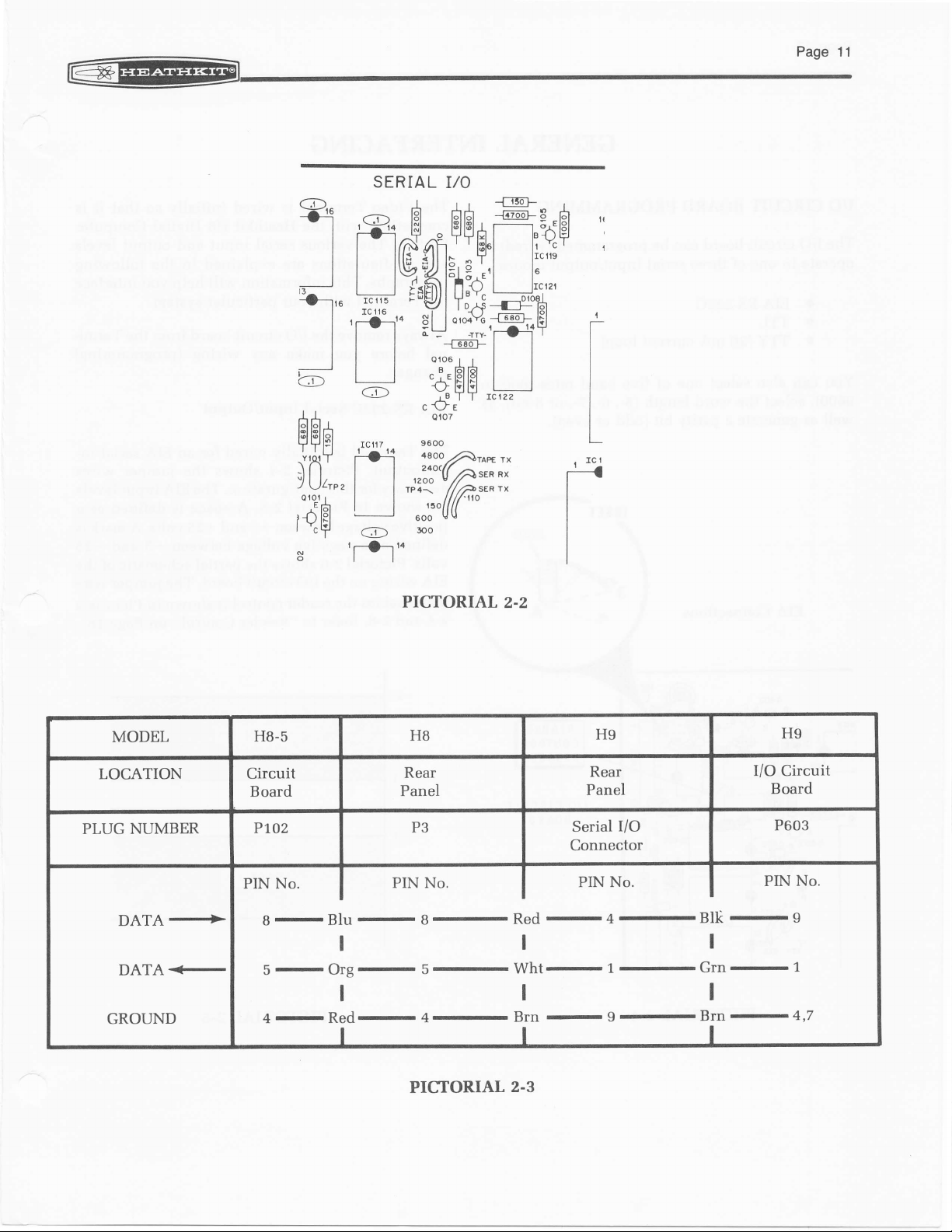
Page 11
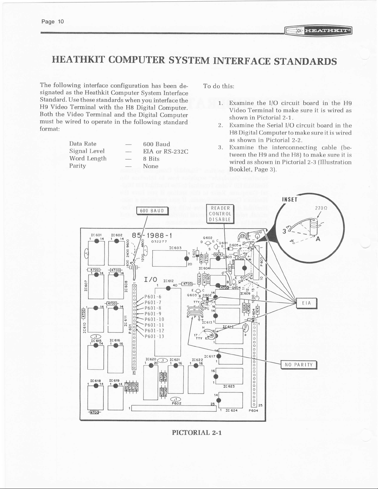
SYSTEM
CONSIDERATIONS
Video
digital
section
Terminal
Refer
System.
computer
"General
the
interface
following
The
Interface Standards"
Heathkit H9
tal
Computer.
Heathkit Computer
Heathkit
minal,
select
refer to
the suitable
"Heathkit
explains
to this
with
Computer
how to
Heathkit
the
to
you
you
your
if
are
H9
section
If
Interfacing"
scheme'
System
interface
HB Digi-
have the
a non-
using
Video
section
the
Ter-
and
Page 12
Paselo
@
HEATHKIT
The
following
signated
Standard.
H9 Video
Both
must be
format:
as the
Use these
Terminal
the Video
wired
Data
Signal Level
Word
Parity
COMPUTER
interface
Heathkit
standards
with
Terminal
to operate
Rate
Length
configuration
Computer
the
and
in the following
System Interface
you
when
H8 Digital
the Digital
600 Baud
EIA
8 Bits
None
600 BAUD
SYSTEM
has
been
interface
Computer.
Computer
standard
RS-232C
or
de-
the
INTERFACE
To
do this:
1.. Examine
Video Terminal
shown in Pictorial 2-1.
2.
Examine
HB Digital
as shown in Pictorial 2-2.
3.
Examine the interconnecting
tween the H9
wired
as shown in Pictorial 2-3
Booklet, Page 3).
READER
CONTROL
DISABLE
STANDARDS
I/O
the
the Serial I/O
Computer to make
circuit board in
to make sure it
circuit board in the
and the HB) to make
il{stT
--
-f',ffi;
-
sure
-\J
--nA
the H9
is
wired
it is
wired
cable
sure
(Illustration
27 0a
/
t
as
(beit
is
r/o
I
"j't.*-H
-6
P60l
P601-7
-8
P60l
-9
P60l
-10
P60l
P60l-lt
P60t-12
-I3
P60t
IC62o
.-1-\ tC 621
i.q-d.sr
|ffit i
t__tffiH
PICTORIAL
2.1
o
o
o
o
o
o
o
o
o
o
o
o
o
o
o
NO PARITY
Page 13
I
-r
__J
bl'.
_l
2-T\
SERIAL
I/O
i
I
MODEL
LOCATION
PLUG NUMBER
DATA+
r*rrir
l,l l.l13l
TTI-I
r'fiT
j
U4,,
OIO_1
,,\.B
IYE
3
H8-5
Circuit
Board
P702
prN
No. I
g-Blu-g-Red-{-Blk-9
IClr7
i-Oi
| |
I lr?4\ ///PosERrx
I
| |
-t
@
'fi'4
l-ll
9600
caoo
l44aft.tx
,,\',J',(n"
"#"u(
3oo
PICTORIAL
H8
Rear
Panel
P3
rt* *o.
^,
2.2
I
t
H9
Rear
Panel
I/O
Serial
Connector
ptN
No.
I
H9
I/O Circuit
Board
P603
plN
No.
DATA
GROUND
{-
g-Org-g-Wht-!-Grn-1
e-Red-
{-
PICTORIAL
[111
2.3
-g-Nyy1
-Q,/
Page 14
t"n"tt
@
I/O
CIRCUIT
The I/O
operate
You
9600), select the word length
well as
circuit board
in
O
o
o
can also
generate a parity
BOARD PROGRAMMING
be
can
one of three
EIA RS-232C
TTL
(20
TTY
select one of five baud
serial input/output modes:
mA
current
bit
GENERAT
programmed (wired)
loop)
(600
rates
(5-,6-,
(odd
or
7-,
even).
or 8-bit), as
INTERFACING
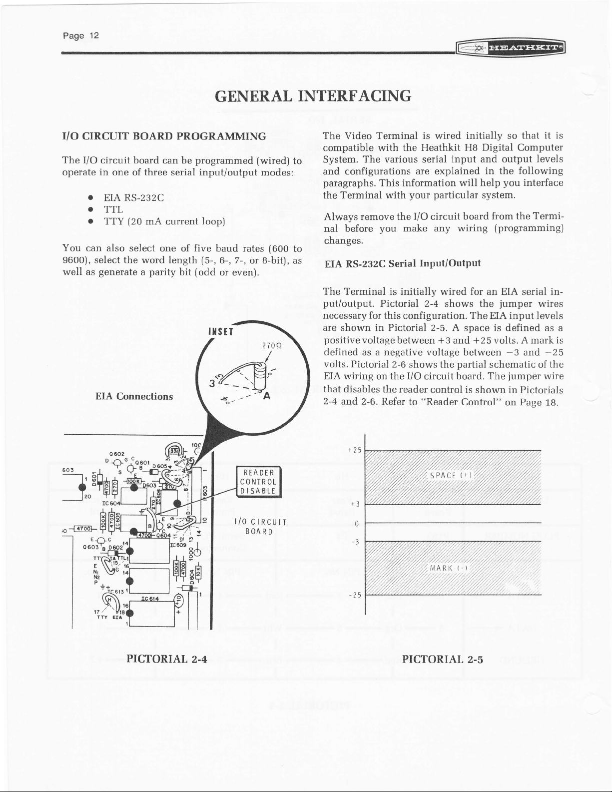
The Video Terminal
compatible with the
to
to
System.
and configurations
paragraphs.
the Terminal with
Always remove
nal
changes.
EIA RS-232C
The Terminal is
put/output.
necessary for this
are
positive
defined as a negative voltage between
volts.
EIA wiring
that disables
2-4
The various serial input and
This information
before
shown in Pictorial 2-5. A
and 2-6.
you
Serial
Pictorial
voltage between +3
Pictorial z-0
the I/O circuit board.
on
the reader
Refer to "Reader
is
wired
Heathkit H8 Digital Computer
are
explained
your particular
the IiO circuit
make any
Input/Output
initially wired for an EIA serial in-
2-4
configuration. The EIA input levels
shows the
control is
initially so that
in the following
will help
system,
board from
wiring
shows the
space
and
partial
Control"
fprogramming)
jumper
is
+25 volts. A mark is
schematic of the
The
shown in
output levels
you interface
defined as a
-3
jumper
on Page
it is
the Termi-
wires
-25
and
wire
Pictorials
18.
PICTORIAL
2.4
RTADER
CONTROL
DISABLE
l/0
ctRCUlT
BOARD
'/t
ACE
sP
ru
7,%,
PICTORIAL
2.5
Page 15
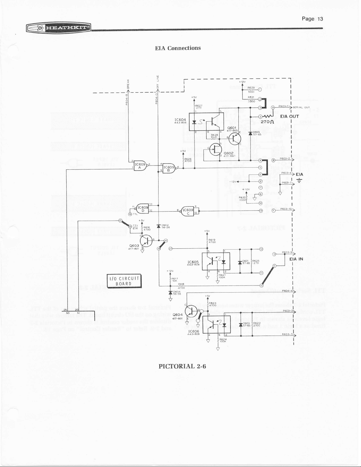
EIA Connections
27On'
Page
13
PICTORIAL
2.6
(r)_lq,3l,>
I
I
I
I
Page 16
14
Page
]-l
77
rc60r
-------_lr
rc 6t2
:"*-H
t
120
oeoirs
@
E-(\c
iL
I
-
icers
TTL
Vi
I
Connections
r/0
BOARD
ctRcutT
+5
t) A
MARK
PACE
S
TTL INPU]
LEVELS
MARK
(LOGIC
(LOG
I C O)
(LOG
IC I)
1)
TTL
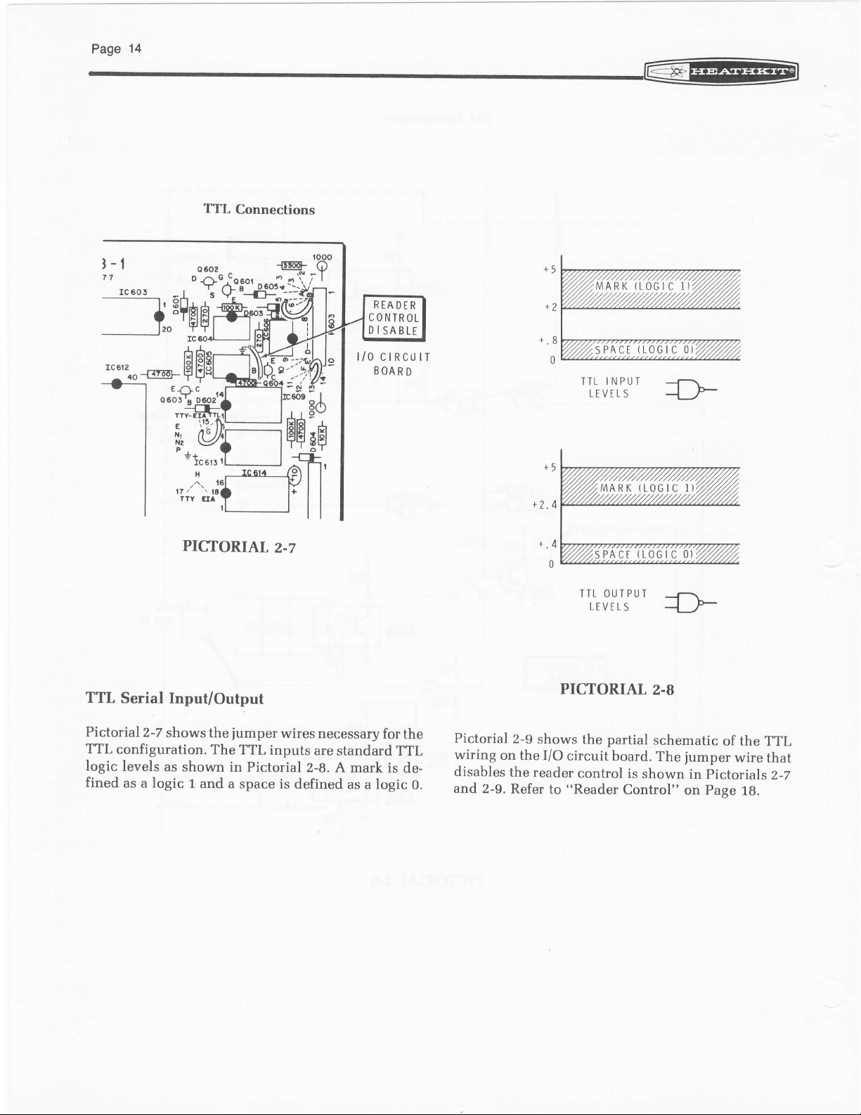
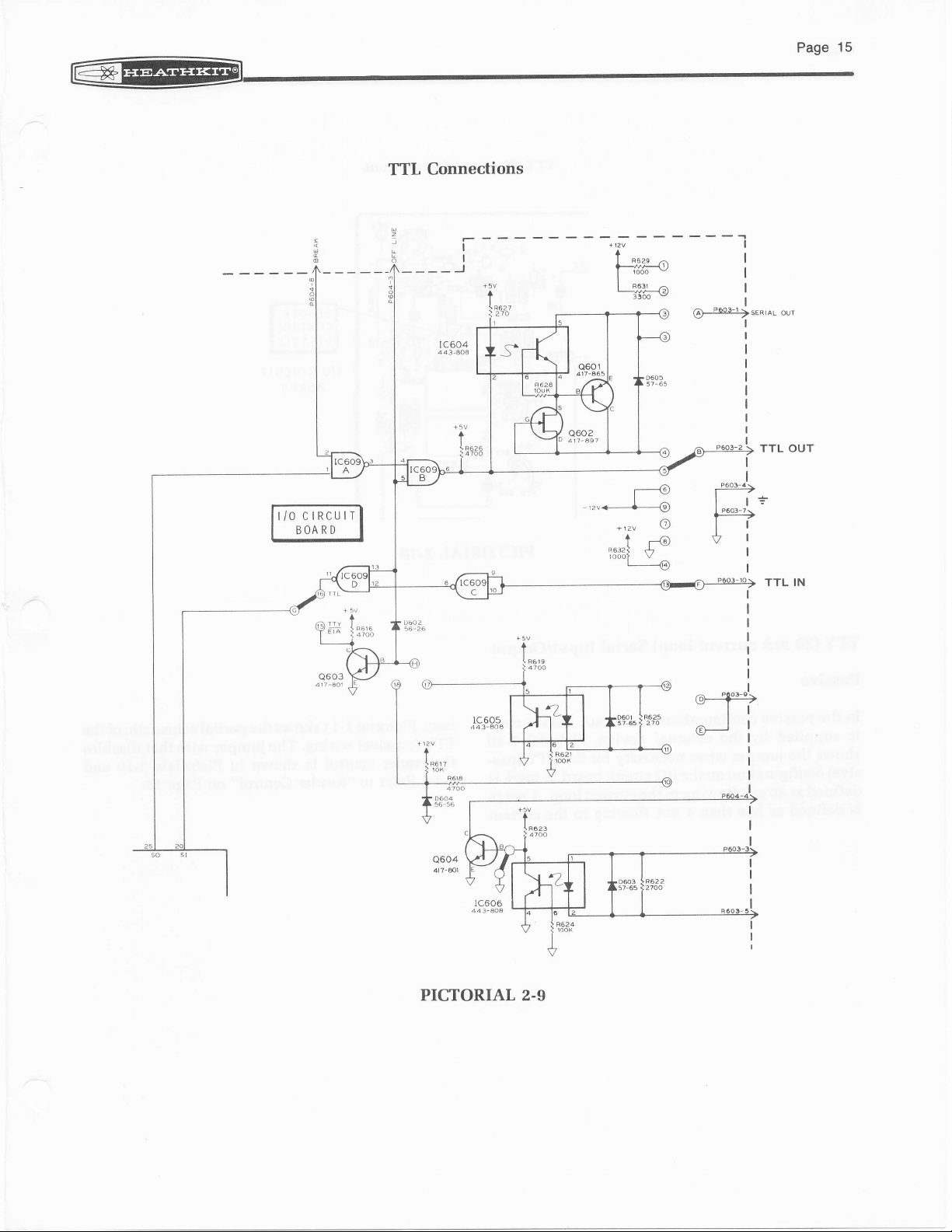
Serial Input/Output
Pictorial
TTL
logic
fined
2-7
shows
configuration.
levels
as shown
as a logic 1
PICIORIAL
the
iumper
The TTL
in Pictorial
and a
space is
2.7
wires
necessary
inputs
are
standard TTL
2-8.
A mark
defined as a logic
for
the
is de-
0.
Pictorial
wiring
disables
and
on
2-9.
2-9
the I/O
the
reader
Refer
+.4
0
TTL OUTPUT
LEVTLS
PICTORIAL
shows
the partial
circuit
control
to "Reader
PACI {LOGIC
2.8
schematic
board.
The
is
shown
Control"
())
of the TTL
jumper
pictorials
in
on Page
wire
18.
that
2-7
Page 17
Connections
TTL
Page
15
z
_---J
tc604
4
43-808
I
I
G"..8'99l:L:sea,ar
our
I
TTL OUT
I
I
tt=
eoe-r>
+12v
ne:zl
IOOO)
O
aa
-
.t'
v
€
vl
I
ll
I
I
IN
TTL
PICTORIAL 2.5
Page 18
Page
16
(Passive)
TTY
-}
o
o
o
Connections
lzo
l/0
ctRcul
BOARD
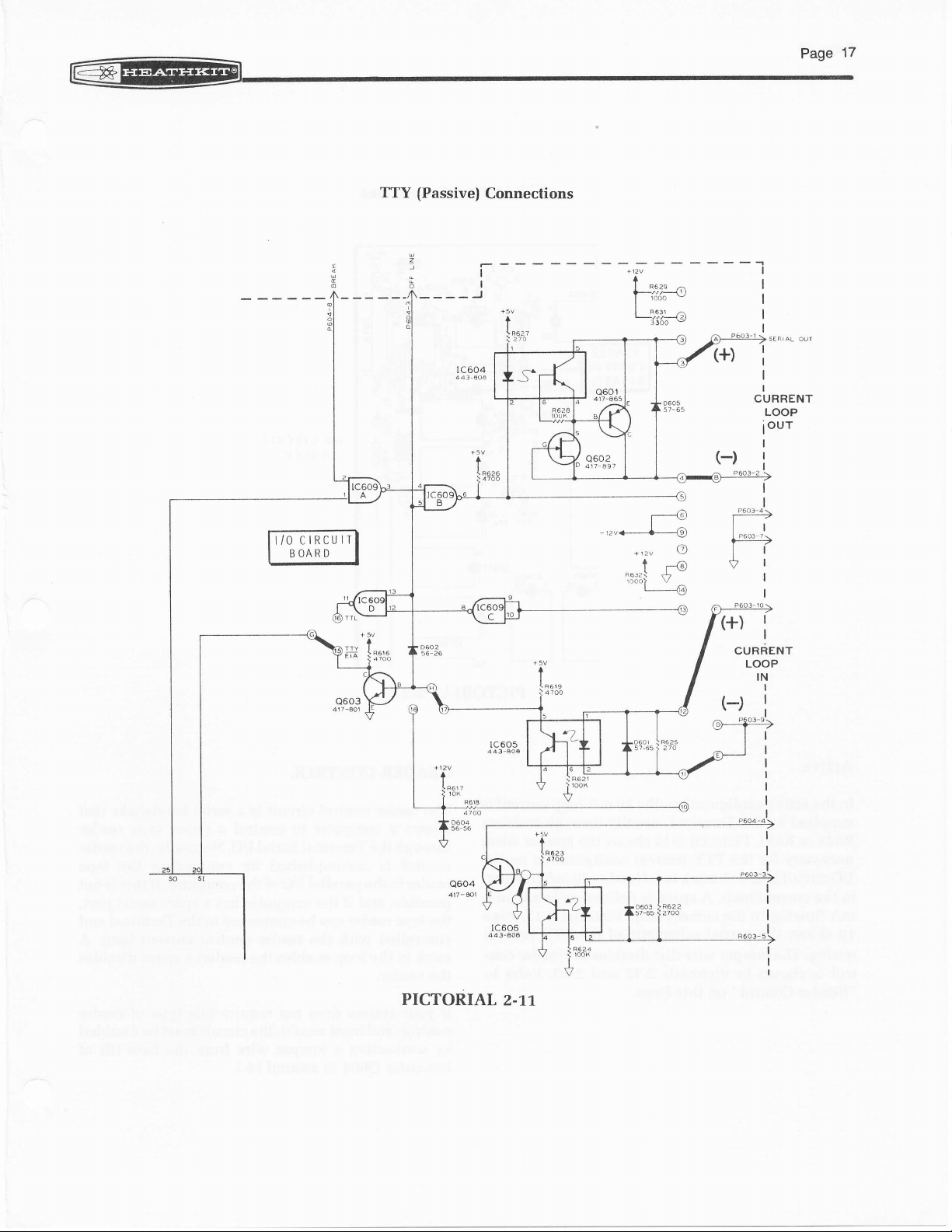
TTY (20
Passive
In
passive
the
is
supplied
shows
sive)
defined
is
the
configuration
as
defined
mA
current
configuration,
by
the
jumper
20
as less
mA
wires
flowing
than
loop)
external
necessary
on the
4 mA
I/O
in
Serial
the
device.
circuit
the
current
flowing
Input/Output
20
mA
pictorial
for
the
board.
loop.
in
PICTORIAL
loop
current
TTy (pas_
A
maik
A
space
the
current
Z_tO
is
2.'],O
loop.
Pictorial2-1.1,
(passive)
TTY
the reader
2-11.
Refer
shows
wiring.
control
is
to "Reader
the
jumper
The
shown
Control"
partial
wire
pictorials
in
on
schematic
that
disables
2-10
page
1g.
of
the
and
Page 19
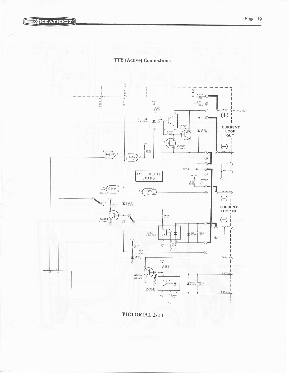
TTY
(Passive)
___-J
1c604
443,604
Connections
I
I
(+)
CURiENT
LOOP
(-)
IN
I
I
I
I
PICTORIAL
2-11
Page 20
Page 18
READFR
CONTROL
DISABLE
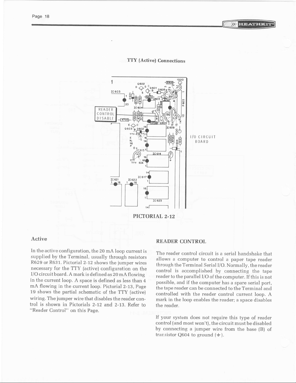
TTY
(Active)
Connections
I/O CIRCUIT
BOARD
Active
In
the active
supplied
R629
necessary
I/O
in
the
by the Terminal,
R631.
or
for
circuit board. A
current loop.
mA flowing
19
shows the
wiring.
trol is
"Reader
The
shown in
Control"
configuration,
Pictorial 2-1.2
the TTY
(active)
mark is
A
space is defined
in
the
current loop. Pictorial
partial
jumper
schematic
wire
that disables
Pictorials
on this Paee.
the 20 mA
usually
through
shows the
configuration
defined
as
of the TTY
2-1.2
and 2-t3. Refer
PICTORIAL
loop
current is
resistors
jumper
20
mA flowing
as less
the reader
wires
on the
than 4
2-13,
(active)
Page
con-
to
2.I2
READER
The reader
allows
through
control is
reader
possible,
the tape reader
controlled
mark
the reader.
If your
control
by
connecting
transistor
CONTROL
control
a
computer to
the Terminal
accomplished
parallel
to the
and if
with
in the loop
systenr does
(and
most
Q604
circuit is
Serial I/O.
a serial handshake
control
a
Normally,
by connecting
I/O
of
the
computer. If
the computer
can be
connected to
the reader
has a
control
enables the reader;
not require
won't) , the
jumper
a
ground (*J.
to
circuit must
wire from
paper
tape reader
the reader
the tape
this is not
spare serial
the Terminal
current loop. A
a
space disables
this type
of reader
be disabled
the
base
that
port,
and
[B)
of
Page 21
ry
TTY
(Active)
___-J
Connections
I
I
SERIAL
CURRENT
LOOP
OUT
OUI
Q604
417-&t
PICTORIAL
2.I3
\!,,
I
I
CURRENT
LOOP
IN
I
(-)
i
I
Page 22
600 BAU D
i2OO
BAUD
24OO BAUD
i-r
0l
ll
.fi?oo]-
t'i
:l
@l
Hl
II
I
I
I
48OO
ir
/{l
t-.tl
'1__J
@l
fi
Ft
ot I
3t I
"ll
n
I
n
BA U D
r98
-
orzr
fi
Y\
la I
+/l
-L
r/o
I
T
I
I
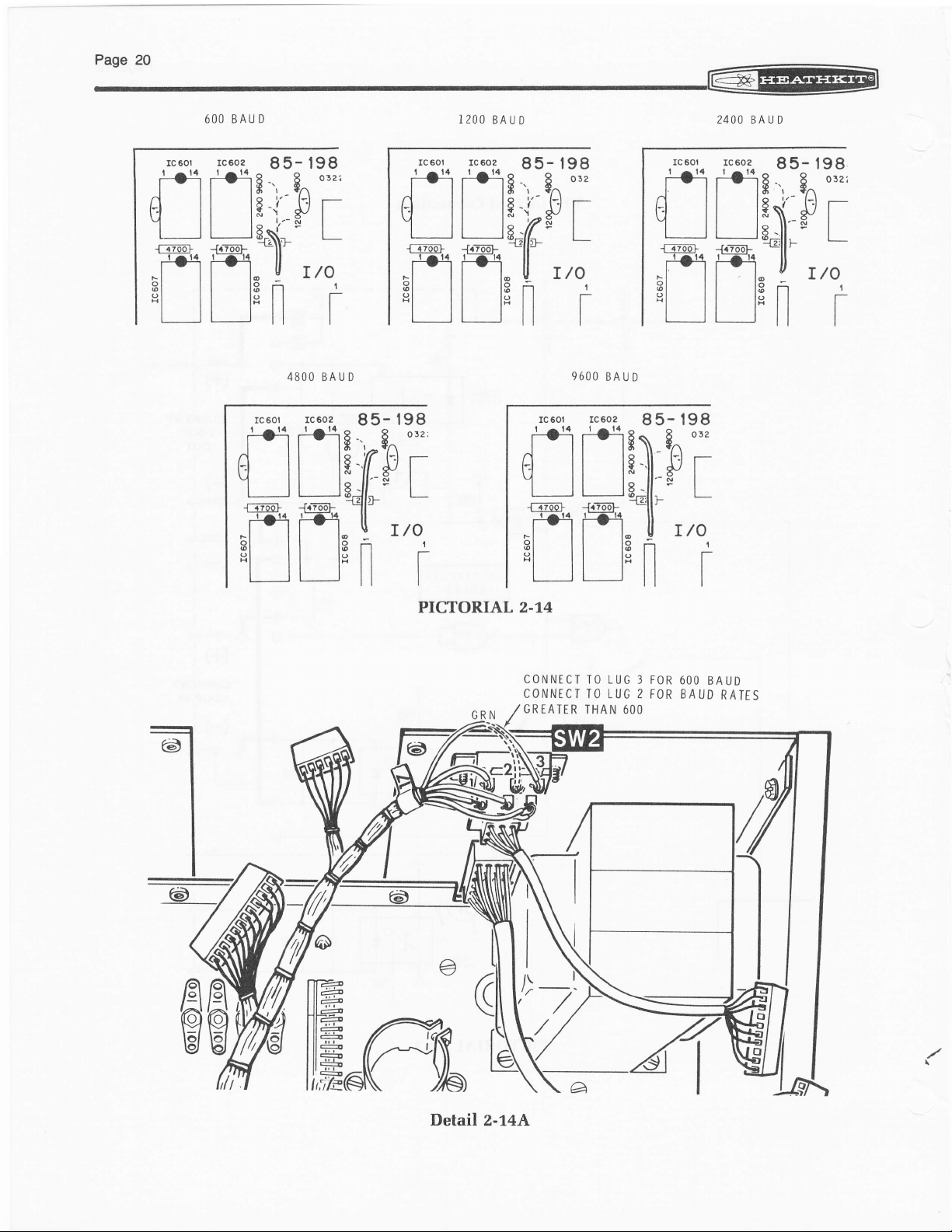
PICTORIAL 2.I4
-
r98
85
I
$
.n
S"'
t--l r-
$/l
.L
}r
I/O
nll
fi
0l
1__J
t"T56l
5t I
sl
-t
tl
o:z
I
T
I
I
9600
I
BA
i.i
0l
'1____l
t"rE6.]-
t''i
Ft
otl
@t
ol
Hl
ll
U D
-
ffinl'
I les-
E*ll'
I
I
I
I lgn
I
$.,
$/l
-L
ll-ll
t98
ott'
[-] r-
T/O
I
T
I
I
6
6
Detail
2-74A
CONNECT
CONNECI
GREATER
TO LUG 3 FOR
TO LUG 2 FOR
THAN 60O
600
BAUD
BAUD
RATES
Page 23
@
Pase21
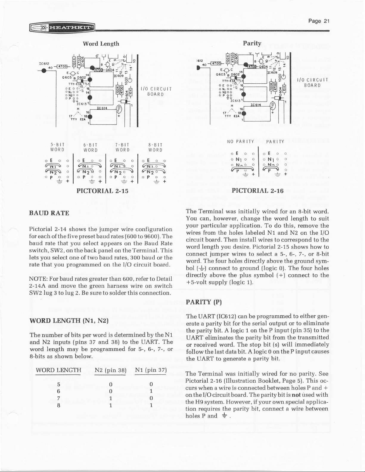
Word Length
A
lol
-r--
"I'10
5- B IT
WORD
oE
ffi
@
"P
oeojr" o
o
i
Er\c
o
o
o
+
$l
oE
ffi
ffi\o
oP
6-BIT
WORD
o
o
=f
PICTORIAL 2.I5
BAUD
Pictorial
for
baud
switch, SWz, on the back
lets
rate that
NOTE:
2-14A
SW2
RATE
2-14
shows
each ofthe five
that
you
rate
you
select one of two baud rates, 300 baud
the
preset
select appears
you programmed
For baud rates
and move the
lug 3 to lug 2. Be
greater
green
sure to solder this connection.
I/O
CIRCUIT
BOARD
7-B
WORD
o
oE
ffio
@
o
oP
.!t
jumper
wire configuration
baud rates
panel
on
IT
o
o o
(600
on the
the Terminal. This
o
to
oE
ffi
,@
oP o o
8-BIT
WORD
9600).
Baud Rate
on the I/O circuit board.
than
harness wire
600,
refer
on
to
o o
++
The
the
or
Detail
switch
Parity
:6!2
;"-*-H
The Terminal
You can, however,
your particular
wires
circuit board. Then install wires to
word length
connect
word. The four holes directly above the
($
bol
directly above the
+s-volt
PARTTY
E-Oc
o603'8
9qo2
YTY.
o
oo\';^'
E
oo'e
Ol{1
o
o
'
N2OO
P
90
=+
rc 6t3
H
^f
.tE
l7/
TTY EIA
NO PARITY
oE
oNlo
o
N^o
e
PICTORIAL
initially
was
change the word length to suit
application. To
from
the holes labeled N1
you
desire. Pictorial 2-15
jumper
connect to
supply
wires to
ground
plus
(logic
(P)
PARITY
o
o
oE
o
o
Nl
O
o N.
m
wired for
select a 5-, 6-,
(logic
symbol
1).
o
o
o
o
o
o
o
+
:
2.16
an
this, remove
do
N2
and
correspond to the
0). The four holes
(*)
connect
l/0 CIRCTJIT
BOARD
8-bit
word.
the
on the I/O
shows how to
7-,
or 8-bit
ground
sym-
to the
woRD
LENGTH
The number of bits
and Nz inputs
(N1,
per
(pins
word length may be
8-bits as shown below.
WORD LENGTH N2
c
6
7
8
N2)
word is determined by
37
programmed
sa) to the UART.
and
for
(pin
38)
5-,
N1
0
o
1.
1
6-,
(pin
0
1,
0
1
the N1
The
7-,
or
37)
The UART
erate a
parity
the
(IC612)
parity
bit for the serial
bit. A logic 1 on
UART eliminates
received
or
word.
follow the last data
generate a parity
the UART
The Terminal
Pictorial 2-16
to
was
(Illustration
can
the
The stop bit
bit. A logic 0 on
initially wired for no
programmed
be
output or to eliminate
the P input
parity
bit from the transmitted
(s)
will immediately
the P input causes
bit.
Booklet, Page
curs when a wire is connected between
your
bit,
parity
bit is
own special applica-
connect
a wire between
on the I/O circuit board. The
the H9 system. However, if
requires the
tion
holesPand
parity
*.
to either
(pin
parity.
5).
gen-
35) to the
See
This oc-
holes P and +
not used
with
Page 24
Pase22
@
oDD/EVEN
This input
is
that
transmitter
A logic o on
immediately after
inserts even
the
Since
is not connected.
input
requires a
odd or
select
KEYBOARD
jumper
A
keyboard circuit
repeat
This is the
ond.
screen when
the
key are
"Repeat
section of
repeat rate.
PARITY
(E)
to
checked
by the
parity
if
E input
the
parity immediately
Terminal does
parity bit,
even
PROGRAMMING
wire connection
rates; 3.7-,
rate at which characters
held down at the same time.
Rate"
this Manual
(E)
the UART
was selected
the data
parity,
board
7.5-,
the REPT
instructions in the
selects
receiver and
as explained
(pin
36) will insert odd
A logic
bits.
after the data
not use the
your
If
Pictorial
lets
\5-, or
(repeat)
if
special
2-77
on the bottom
you
30-characters
you
want to change
select one of
key and a character
the type
generated
1
parity
shows
are written on
"Readjustment"
parity
of
by the
above.
parity
input
this
on
bit, the
application
how to
of
per
Refer to the
bits.
the
four
sec-
the
Odd/Even Parity
E
t/0 ctRcutl
BOARD
PAR Y
EVENPARITY
(ffiJ
oNlo o
o
N2o
oP o
++
ODD
ao
o o
o
Nl
o
o
o
oP
N2o
++
o
o
o
TYPICAL
Parallel
following
The
the signal
panel.
rear
the
PIN
#
7
2
3
4
5
6
7
8
I
TERMINAL/COMPUTER
Input/Output
Connections
parallel I/O connector
ofthe
parallel
Parallel
Output
Take Data o
pin
each
on
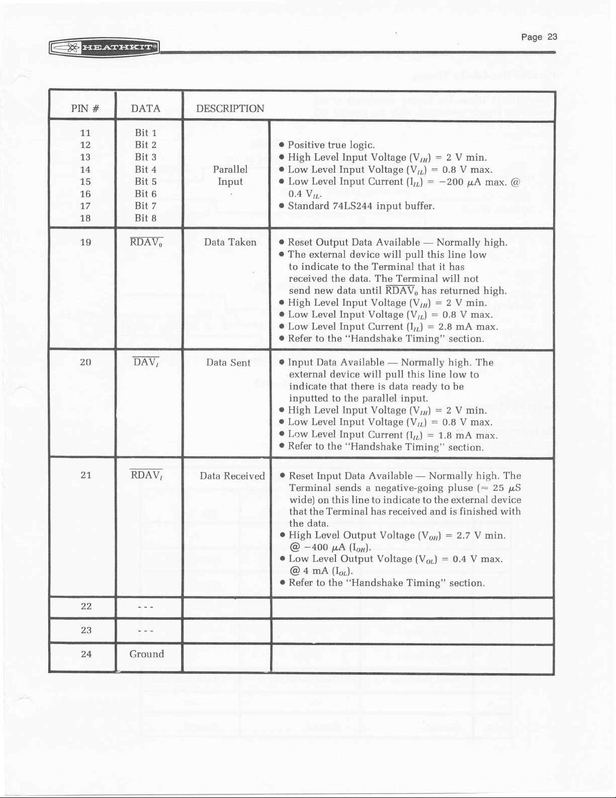
DATA DESCRIPTION
Bit 1
Bit 2
Bit 3
Bit 4
Bit 5
Bit 6
T
BiI
Bit 8
DAVo
SYSTEMS
describes
chart
I/O connector
o
o
o
o
r
.
.
on
Positive true logic.
High
Level Output Voltage
(High
pA
LowLevel
(Low
Level
Output Current).
OutputVoltage
Level
Output Current).
Standard 74L5175
Available
data
Data
will hold
available
at
Output
Terminal
is
device.
HighLevel
(High
p.A
Low
(Low
Refer to the
OutputVoltage[Vr")
Level Output
Level Output
Level Output
"Handshake
PICTORIAL
latches.
- Normally
this line
parallel
the
CurrentJ.
Voltage
Current).
(Vo")
:
(Y
ot\
low to
output
:
:
[Vor)
Timing"
2.I7
:
2.7 min.
0.4 Vmax.
The
high.
indicate
that there
for the external
2.7Y min.
V max.
0.4
section.
@
@
Video
@
@
-400
amA
-400
a mA
10
Page 25
@
-
Pagezs
PIN
#
17
72
13
74
15
16
77
18
19 mAv; Data Taken
20 DAV;
DATA DESCRIPTION
B
t1
B
t2
B
t3
B
t4
B
t5
B
t6
B
t7
B
t8
Parallel
Input
Data
Sent
o
Positive true logic.
o
High Level Input Voltage
o
Low Level Input Voltage
.
o
.
o
o
o
.
.
.
Level Input
Low
o.4
vL.
Current
Standard 74L5244 input
Reset
Output Data Available - Normally high.
The external device will
to indicate
received
the data.
send new
data until n-Dffz, has returned high.
to the
Terminal
The
High Level Input Voltage
Low Level Input Voltage
Low Level Input
Refer to
the
Current
"Handshake
Input Data Available - Normall5r
external device will
indicate
that there
inputted to the
o
High Level Input
o
Low Level Input Voltage
o
Low
Level
Input
o
Refer
to the "Handshake
is
parallel
Voltage
Current
(Vr")
(Vrr)
(Irr)
buffer.
pull
that it has
Terminal will not
(Vnt)
(Vrr)
(Irr)
Timing"
pull
this line
data ready to be
input.
(Vrrr)
[Vrr,)
(Irr)
Timing"
:
2
V min.
:
0.8 V max.
:
-2OO
p"A
this line low
:
2 V min.
:
V max.
0.8
:
2.8 mA
max.
section.
high. The
low to
:
2 V min.
:
0.8 V max.
:
1.8
mA max.
section.
max.
@
27
22
23
24
m-AV,
Ground
Data Received
.
o
.
.
Input
Reset
Terminal sends a negative-going
wide)
that the Terminal has received and is finished with
the data.
High Level
@
Low Level
@
Refer
this line to indicate to the external device
on
-+oo pA
(Ior).
4 mA
to the "Handshake Timing"
Available - Normally high. The
Data
pluse
:
Output
(Ior).
Output
Voltage
Voltage
(Vo")
(Vor)
2.7 V min.
:
0.4 V max.
section.
(:
25 p,S
Page 26
Parallel
Handshake
Timing
Pictorial
2-18
handshake
port.
DAV0
I NAL
TERM
RDAVO
TXTTRNAL
DAVI
EXTERNAL
RDAVI
IERMINAL
shows
signals
the timing
associated
LOW LTVEL
RDAV-o RESEIS
LOW
waveforms
with
the
SAYS
"DATA
LOW LEVFL
DATS
LFVEL
SAYS
of the
parallel
SAY S
I/O
Handshake Timing
READY FOR
'' I'VE GOT
HAVE DAIA
PICTORIAL 2.IB
EXIERNAL DEVICE.
I I.
"
FOR YOU.
_rlZl.susk_PULSE
-t--'---l
''
SAYS ''ALL
rvrusT
IITr
OF TRAILING EDGE
SAYS "I'VE
HrGH wtTHrN
co
TAKEN
DONT.
OF PULSE
THE
DATA."
''
r4us
Serial
The
signals
rear panel.
I/O
following
on each
Connections
serial I/O
pin
PIN
#
7
2
3
4
5 Reader
6 Reader
connector
of the
TTY
AND
Serial Out
Serial Out
Serial
Serial
Baud Rate
serial I/O
(ACTIVE
PASSIVEI
[+)
(-)
(+)
In
In
[-)
(+)
Start
(-)
Start
Out
chart describes
connector
SERIAL
the
on the
PORT NOMENCLATURE
EIA RS-232C
Serial
Serial In
Baud Rate
Out
Out
TTL
Serial Out
Serial In
Baud Rate
Out
B
9 Ground
Ground Ground
Page 27
@
U
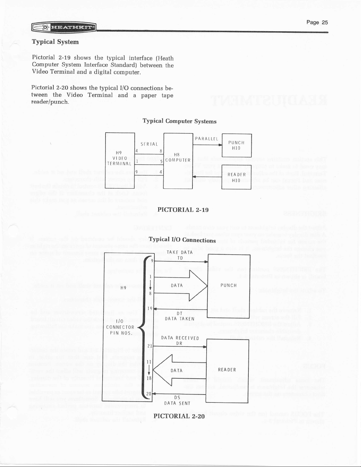
Typical
Pictorial
Computer
Video
Pictorial
tween
System
2-L9
System Interface
Terminal
2-20
the
Video
reader/punch.
shows the
and
a digital
shows
the typical
Terminal
typical
interface
Standard)
computer.
I/O connections
and a
H9
VIDEO
TERMINAL
fHeath
between
paper
Typical
SFRIAL
4
I
I 4
the
be-
tape
Computer
8
H8
COMPIJ
5
TER
PICTORIAL
Systems
PARALLFL
2.1,5
PUNCH
H10
RTADFR
Hr0
H9
t/0
CONNECIOR
PIN
NOS,
Typical
TAKF
DATA
DATA
,L
\
\l-
DATA
I/O
Connections
DATA
ID
DT
TAKEN
RECEIVED
DR
DATA
DS
SINT
PUNCH
READER
PICTORIAL
2.2O
Page 28
Pase26
READIUSTMENT
@
to suit
your
periods
(on
with
characters.
adjustments
maintain
(except
separately without
your
when
eyes
of time. Whenever
video
the
This section
need to
may
Terminal. Each of
ness and
affecting other
BRIGHTNESS
Adjust the display brightness
A dim display
the screen
you
change the
readjust
The BRIGHTNESS control
board) is shown
To adjust the brightness:
1.. Remove the cabinet shell and set it aside.
2. Fill the
3. Adjust the BRIGHTNESS control to
4. Reinstall the
contains
make to
Focus) can be adjusted
adjustments.
is
for
extended
focus.
the
desirable character brightness.
several
properly
the adjustments
easier on
brightness, it is also a
in Pictorial 3-1.
screen
cabinet shell.
that
your
for Bright-
needs.
own
you
look at
good
idea to
circuit
obtain
you
Video
To adjust the focus:
1. Remove the cabinet shell and set it aside.
2. Fill
3. Adjust the FOCUS
4. Reinstall
CENTERING
The display
should have the
it does
the top
To
adjust the
1. Remove
2. Fill
NOTE: Use an
a
careful
or
adjustments.
the screen with characters.
focus. Look
and
corners of the screen as
adjustment.
should be centered
same amount of space on the right
on the left, and the
it
as
does
on the bottom.
centering:
the cabinet
the
screen with
you
do not touch
the anode lead
the
at
the cabinet shell.
same amount
insulated screwdriver
when
control to obtain the best
characters at the
you
on the screen. It
shell and
characters.
the video circuit board
you
make the following
set it
edges
make this
as
of space on
aside.
and be
FOCUS
focus adjustment,
The
whenever
tinct characters
The
shown
the brightness
Pictorial
in
control
FOCUS
which should be made
is readjusted, assures dis-
on the screen.
(on
the
3-1.
video circuit
board) is
3. Refer
4.
to Pictorial
ing magnets,
center the
the
centering
cal and horizontal
use the minimum
(magnet
that is necessary.
to
and
Reinstall
tabs
compromise
perfect
the
3-1
first
display
magnets
linearity
spread as far apart
Sometimes
between
linearity.
cabinet shell.
rotate
and
one, then the
on the screen. Because
will affect the verti-
amount
perfect
the center-
other, to
of the
display,
of correction
possible)
as
you
will have
centering
Page 29
@
,'ilIli^ll,'\
t0cus
BRtGilTlttss
_
t"n"tt
\\
\\
\
HEIGHT
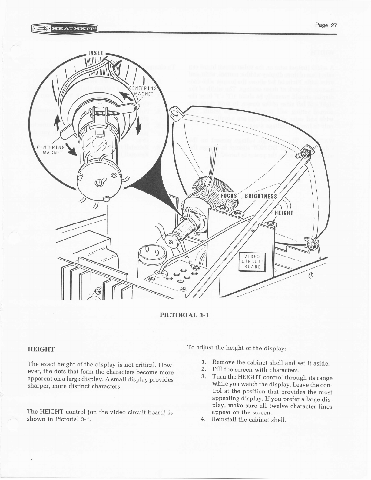
The
exact
ever,
the
apparent
sharper,
The
HEIGHT
shown
in
height
dots
that
on a large
more
distinct
control
Pictorial
,6-
of the
form
display.
characters.
(on
3-1.
display
the
characters
A
small
the
video
is not
critical.
become
display provides
circuit board)
e
€e
e
-@
PICTORIAL
To
How-
more
is
3.1
adjust
1..
2.
3.
4.
the height
Remove
Fill
the
Turn
the
while you
trol
at
the
appealing
play,
make
appear
Reinstall
on the
of the
the
cabinet
screen
HEIGHT
watch
position
display.
sure
the
cabinet
display:
shell
with
characters.
control
the
display.
that provides
If you
all
twelve
screen.
shell.
and
set it
through
Leave
prefer
character
a
large
I
lt
aside.
its
the
the
range
con_
most
dis_
lines
Page 30

Pase28
WIDTH
@
A width
select one of three display widths;
extra wide. Pictorial
nection for
display should normally
right
normal
wide
only
WARNING: There
video
width
jumper
and left
setting will
and extra wide settings are usually required
in low
circuit
jumper
wire on the
3-2 shows the
each of these settings. The
sides of the screen. In most
provide
line voltage areas.
is high voltage
board. DO NOT attempt to change the
when the
video
circuit board can
normal, wide, and
iumper
be about L12' - 7'from
adequate
present
power
is
turned on.
wire con-
width of the
the
cases, the
width.
The
on the
To
change the
7. Turn the
2. Remove
3. Remove the video
4.
5.
6, Reinstall the
7. Reinstall
display width:
chassis.
Pull the
pin.
Insert
the
pin
that corresponds to
sire.
ON/OFF switch to OFF.
the cabinet shell and set it
circuit board from the
jumper
the cabinet shell.
wire
jumper
wire into the
circuit board
out of the connector
connector
width
the
in
the chassis.
aside.
you
de-
Page 31

Page
29
-@
A
-{roKi+
-{2700
-l-
rSlFlr----r
t8|llt I
l!l
l-l
lol
tol
F t= |
T
F-TH
IC 301
cDl
, lol
6t ll
lEl l$ |
-r-
@
8fF
BRtGHTNEss
.
r5$l-A
lflry*?
VIDEO"-
-.
l,\/CATlloD€1-r
_l T-l
:
I lsl _
I l:l J
J
D,?
f
'
\
I
-.1
/
[$|
LJ
'
-
11999_f
a^@+r.g
(
3d.
"J
\17
rrn,l$l-@
lsll
ll
|
| | I
'll
rll
ll :A
-!-
z.z
.ll--r---i
r*,-
r'P,[J.o%o..
toKF
:-
+E
(
\t--l
r. )
;l
ol
,oo
-+-
I
{ro-6-Ff
]TTEf
)-
3E-
@
-f;;-;;L
'A'i*
R!
rn
ll li I.- il ll I
wrDrH
ll ll
j
lt-------el
ll l/-\/\l
l--
*@
$ll ll
*ll
ll ll s ll B | | r_
[]UU
s
ll ll I
'o
il
'
-ll
=-
rocus
rir
-o-
l5l
teq
t1!-!!-f
@
-fs-
L 3Ol
ll I
ll I
GD
VIDEO
CIRCUIT
BOARD
I
ll
ir
II
ll
l"l
-r
GD
: lpll ll
(*)'glii
)
-V
;3 illao
#II IUU
PICTORIAL 3.2
@
s-
@
;i?iiiiivT;El r rrs-----
H'il llE:;
iill
I lr
o5o7 '?t'
-F
GD
I
I
Page 32

Paseso
@
REPEAT
When
held
peatedly
set at 3.7,
rial 3-3 shows the
bottom of the keyboard circuit board) for each of the
repeat
to determine which one best suits
To
change the
RATE
the REPT
down
written
rates.
Turn
7.
2. Remove
(repeat)
at the same time, the character is re-
on
7.5,
\5, or
You may want
repeat rate:
the ON/OFF switch OFF.
key and any character
the
30
fumper
bottom
the
screen.
characters
The repeat rate can be
wire connection
try
to
all of the
panel
per
second.
your
and set
key are
Picto-
(on
the
repeat rates
needs.
it
aside.
Pull
3.
pin.
4, Insert the
pin
desire.
Reinstall the bottom
5.
CLEANING
You
cloth to clean
the dust
smudges still remain,
with a mild soap and a soft cloth. Be careful
not scratch the
can
use
from
jumper
the
that corresponds to the repeat rate
mild household detergent and a soft
any
the cabinet
the
plastic
jumper
of
window
clean
window.
wire out of
wire into the connector
panel.
the Video Terminal. Wipe
with
the window
the
a soft
connector
cloth.
carefully
you
you
If
do
Page 33

{ } F-----t
b iltb I
D |rp I
v-
v-
@4
p
Ju,,,il
to/
N/
PE
RE
\\
tD)
Page
31
N
o
N
€
o
N
In
o
_A
btDl
b I P |
::
r-----------1
:
:
||
I I
t-
--+-
n- n- n-nl
tffitrFF'ltrFFlf1l
IFll=l{l{l=ll--ll
ll se
Eo
=IHHF{
-
_)fr.
/<)
2/
-l
rlg
ril=
IH
ru
tffi
rtrtr
r-]i
\(Jl
I
=
I
o
-
-
e
E
PICTORIAL
3.3
Page 34

SPECIFICATIONS
..
CRT
Display
Keyboard
Interfaces
BAUD Rates .
Characters
Format 960
phosphor.
72" diagonal,
panel
filter.
characters.
characters.
67 keys including: 52-key
5 cursor control
10
(full
Serial
EIA/RS-z32C
(20
TTY
TTL
Reader
Parallel
8-bit input
8-bit
4 handshakes
Seven, user selectable - 11"0, 300, 600, L200, 2400,
4800, and
x
7 dot matrix. ASCII
5
bers, and
P4
Normal
form
Short
special
(TTL
output
function/mode keys
or half duplex):
mA current loop)
Control
9600.
punctuation.
(20
loads):
keys
mA current loop)
Glare-free
-
mode
- 48 lines of
ASCII
upper case alphabet, num-
neutral
lines of 8O
tZ
20 characters.
keyboard
front
OperatingTemperature.,..
Power
Voltage Requirements . .
Dimensions
Weight
Requirements . . . . 120 VAC,
. L20 VAC
The Heath
instruments
without incurring
feautres in
0oto40oC.
24O VAC,5O16O H2,50
240 VAC
15-518'W
(39.7 x
32
Company leserves
and to change
any
instruments
specifications at any time
obligation
previously
(100
(2oo
52.7 x 31.8 cm.)
(1+,5
lbs.
the rightto
to incorporate
sold.
Hz,
50/60
-
- 27o VAC),50/60 Hz.
x
2o-3l4n D x 12-\l2tt H.
kg).
discontinue
watts.
50
watts.
135 VAC),
new
50/60
Hz.
Page 35

@
-
TROTJBLESHOOTING
This
section of the Manual
The first
mation,"
may
Terminal.
part,
describes
occur
titled
during
"General
what to
or right
is
divided into
Troubleshooting
do
about difficulties
you
after
assemble
four
parts.
Infor-
that
the
The
Waveforms,"
and their respective
blank,
waveforms.
third
always
section,
provides
test
check the
Page33
titled "Troubleshooting
several
important
points.
horizontal
If
waveforms
the
CRT screen is
and vertical
svnc
The
second
problems
lists
"Possible
sociated with the
the circuits involved
will help
this
and
Circuit
part,
titled
or conditions
Cause"
column lists
problem.
you
relate a
Description.
"Troubleshooting
that might
the components
In
many
with the
problem
problem
Charts,"
occur. The
as-
cases, the name
are also
to the Schematic
given.
of
The fourth
plains
Refer to
of
parts
how to
the
on
part,
titled "Shipping
prepare your
"X-Ray
the circuit
Views"
Terminal
for the
boards.
Information,"
for
shipping.
physical
location
ex-
Page 36

t"n"to
@
General
NOTE: The following checks will
you
apply them to one
1,. Recheck the
pencil
frequently helpful to have a friend check
work. Someone
may notice something
overlooked.
2. About
do not function
tions
can
connections
described in the
beginning of the Assembly manual. Reheat
doubtful connections. Be sure all wires are soldered at
nected.
3.
Check each circuit
no solder bridges between adjacent connections.
clean soldering iron tip between the two
that are bridged until the excess solder flows
down onto the tip
on the Pictorial as it is checked. It is
of the kits that are
90%
and
soldering.
be
eliminated
places
Remove
part
of the kit at a time.
wiring. Trace
who is
properly
to make
"Soldering"
where several wires are
board foil to be sure there are
any solder bridges by holding
of the soldering iron.
familiar
not
you
due to
Therefore,
by a
careful
sure
Troubleshooting Information
be
most effective if
lead in colored
each
with
have
returned
poor
many troubles
inspection
they are
information
your
the
unit
consistently
for repair
connec-
soldered as
at the
any
con-
points
of
Be
5.
6.
sure each diode
positioned
end
Check all component leads
cuit boards. Make sure the leads
through the
with
7.
The
other connections or
components listed
circuit board
column of the
most likely
causes
causes) of a
components, look first
Parts installed
pertains
This
trolytic
and tantalum capacitors,
is
installed with the banded
correctly.
connected to the cir-
and come in contact
parts.
"Possible
in the
"Troubleshooting
(but
not necessarily
problem.
When
for the following items:
incorrectly
especially to diodes,
do not
extend
Cause"
Chart" are the
the only
you
check these
or backwards.
and trans-
elecistors.
Unsoldered
Reheat
the connections in the area of a
inadequately
or
soldered
parts.
problem.
a
Incorrect
part
numbers
interchanged parts.
or
on the diodes and
Check the
transistors.
4.
Check each
that is discolored,
bulging would indicate that it is faulty and
of
should be
resistor value
cracked,
or
replaced.
carefully.
shows any sign
or
A resistor
NOTE: In
resolve
information inside
"Warranty"
an extreme case where
a difficulty, refer to the
is
located inside the front cover.
the
rear
cover
you
are unable to
"Customer
the Manual. Your
of
Service"
Page 37

ry
-
POWER
SUPPLY PROBLEMS
CONDITION
1. Nothing happens
2.
Fuse blows.
3. No s-volt output
low).
TROUBLESHOOTING
at turn
on.
or s-volt supply incorrect
(too
high
or
too
CHARTS
POSSIBLE
1. Terminal not
2. Fuse
3. Primary/line
4.
5. Fuseholder wiring.
6. Power
1.
2.
3. Short circuit
4.
5. Check for
6.
7 .
8.
9.
10.
1. |c101,lct02.
2. D101 - D104.
3. C1.
4.
CAUSE
plugged
F1 blown.
Switch 51 wiring.
Check
Short circuit on the
Shorted rectifier
and C105.
Shorted
Check
sink.
Incorrect
Power
Shorted regulator
+s-volt
cord wiring.
transformer T1.
primary
wiring.
across lransformer
shorts at the outputs
regulators.
for
a short between
fuse.
transformer.
reference
in,
power
supply circuit
diodes. D101-D1 12.
of the bridge rectifiers.
1C101,|C102,
the collector of
outputs. P101-1 , -2, -3, -4, -5, &
(ground)
$
not
board.
secondary.
1Cl03.
Q101 and
grounded
at P101-6.
C1, C2,
the heat
'1
.
-1
4.
+12
No
5. No - 12 volts,
6. No
7.
No
No
8.
CAUTION: Measure the
high voltage
volts,
or it measures too
or it measures
+26
volts,
or it measures
+36
volts,
anode voltage when
or
probe..
it
measures
high
too high
too high
too high
other voltages
high voltage only with an
low.
ortoo
low. t.
or too
or too low. 1.
too low.
or
are OK.
approved
1. lf
2. lf the
+26-volt
the
will
also be
26-volt supply is
reference
1c105.
2.
R105 and
3.
D109 - D1 12.
4.
C107 installed
-
5.
2. R103
3.
4.
5.
't.
2.
3.
1.
2.
3. 1c301.
4.
5.
12-volt
tc103.
and R104 interchanged
Q101, Q102.
D105 - D108.
+26-volt
c2.
D105 - D108.
Transformer
Flyback transformer T2.
Q1, Q307.
L301, deflection
Shoried
supply
low.
ground.
interchanged
R106
backward.
reference
reference
T1.
yoke.
foil
on the video
is
+15
below
OK, check 1C104 and the
volts,
or wrong values.
ground
ground
grounded
not
or wrong value.
grounded
not
circuit board.
+12-volt
the
at P101-6.
at P101-12.
supply
+12-volt
Page 38

Pase36
@
CONDITION
9.
10.
VIDEO
CONDITION
1 1. No video
12.
-150
volts is incorrect.
+400
volts
is incorrect.
RELATED PROBLEMS
(blank
screen).
Screen all white
(raste|.
POSSIBLE
1.
2.
1.
2.
3.
POSSIBLE CAUSE
1. Anode voltage incorrect,
2.
3. No
4.
5. lC222A
6. Videoiblanking
7.
8.
1.
2.
3" tc222A.
4. Videoi
5. Brightness
CAUSE
D304.
c323.
R335.
D305 - D307.
c324 - c327.
Grid voltages incorrect
cathode drive.
Q308, Q309.
Brightness control
lC217A
Check
Q308 or Q309 shorted.
blanking chain on the character
out
1Viffi
(blanking in).
grid
of character
chain on the character
R338
voltages.
control R338 turned up.
(G1,
G2, G4).
generator
turned down.
circuit board).
qenerator
generator
circuit board.
circuit board.
13. lnsufficient
14. A
single bright horizontal line
15. Too
16. Too much
17. No horizontal
18. No vertical
brightness or contrast. 1.
much or too little heioht.
to little
or
sync.
sync.
width.
Q308, Q309.
2. R342, R343.
3. C328, C329.
4.
Check
appears on the screen. 1. Vertical
2. Deflection
3.
Q301 - 0306.
4.
lC221A
1C216 (sync/frame
5.
board.
1.
Height control R303
2.
Q301, Q302.
3.
'1.
2.
3. Deflection
4. Flyback
1.
2.
3. 1c301, lc2114.
wrong value
C303
Adjust
C321.
R325.
C312,C314.
1. lc221A.
2.
Q301.
grid
voltages.
amplifier.
yoke
(vertical),
(V
sync)
on
counter) on the character
or installed
jumper.
width
yoke
1301.
or
transformer T2.
the
character
misadjusted.
backward.
generator
circuit
board.
generator
circuit
Page 39

CHARACTER
WRITING
PROBLEMS
CONDITION
19.
Characters don't
write
on
20. Wrong characters write
the
screen. 1. Duplex
the
on
screen
POSSIBLE
1. DAV latch
DAV
3.
4.
Three-state enables
5. RAM WE. OC
6. RAM
7. DAV from lC719C, lC725A, lC713C.
8.
Special
(A1
or
1. Keyboard
2. Keyboard
3. Bus wires interchanged.
4.
Bus wires shorted to + or
5. Bus
buffers
6. Shorted bus
7.
BAUD rate set wrong.
21. Screen filled with same character. 1. RAM
2. Keyboard
P402-8 always logic 0.
Check
Parallel input
3.
above.
4.
UART ilDE enable always on: Check
above.
CAUSE
switch
(1C616)
priority
F. OC
character
A2 high).
encoder
buffer
in
No DAV
-
encoder
(1C61
(1C6088,
if
DAV timing
if DAV riming
generator
1C402.
1C403.
when it
signal.
1A,
C,
C, D).
pulse (lC737A).
pulse (1C7198,
l@04, 1C405, 1C406 latched
"full"
position
ground.
1C603, 1C620.
foil.
counters
not
counting:
tc722o, D.
tcs02.
tc219F, tc217D.
output enable always on:
DAV latch
and three-state enables
tc616. tc608. tc610. tc619.
enable always on: Check
"half".
should be
D, lC610D, lC619B).
items listed
items listed
in
D).
under
under
on
2
2
22. Same line is repeated 12
23. Blocks
24. Writes
25. Characters write
26. Misses
27.
28. Writes
of characters are repeated
two characters. 1. Full Duplex key
erratically.
characters coming from the
Characters
write in more
control characters.
times. 1.
left
right. 1.
to
computer.
than one
position
on the screen. 1. Address
+12
2. 1c519,lC511C, rcs158, rC716A, rC715C.
2.
'1.
1. Refresh interrupt not
2.
counter not cbunting up.
+4
1c513, lc5148,
duplex
Wrong baud rate.
switch. Connect
great€r
At 110
stop
counter
(pushed
than
baud, the
bits.
not
counting.
600).
lcs10C.
set
in).
the
encoder.
for half
enabled at the
gr6en
wire to lug 2 of SW2
computer
(released)
duplex
may not be
rear
programmed
1C512, lC526A, lC526D,
2. RAM address lines shorted or open.
"Conditions
3. Counters
4.
Check
+4, +4 + +12, +QQ e +12,
't.
Control character decoder.
not
counting up
the counter cascade controls.
(see
lC73O,1C724
etcl.
lC703C, lC703B, lC707C, and
tc702.
2.
Control character detector.
lC617A.
baud
full
rate
rates
instead of
pqnel
(for
BAUD
lor two
& lC527B.
22 & 23" above).
+
(+20
Page 40

Pase38
@
CONDITION
29. Writes wrong
30. Cannot write from the keyboard.
31. Control characters
character
do not blink in
CURSOR PROBLEMS
CONDITION
No
32.
cursor. 1. Cursor coincidence
33. No
screen.
34. Cursor controls will not move
cursor
movement
from keyboard
plot
mode. 1. No
when characters are written on the
cursor.
POSSIBLE CAUSE
1. Shorts between the X and Y scan and address lines
keyboard
2. tc402, 1c403.
1. No
2. Keyboard
2.
Control character video/decoder. lC201A, IC2O7B, lC210D,
tc219D.
POSSIBLE CAUSE
2. TPU cursor
3. Character
tc218B.
No
1.
+20
2.
+20
3.
1. 1c727.
2. No 1C
3.
Cursor
4. Q401.
encoder. 1C402.
(OE).
enable
output
3.75
-:20
counter.
count uo defeated. lC708D. 1C720. lC729A.
harness
bus
Hz. lC741D, 1C401.
gates.
generator
count up.
1C502.
pulse.
1C728.
movement latches
lC608D, lC611D, lC6198, 1C616.
plug
P402 disconnected.
gate.
lC710C,
cursor chain.
lC734B
1C508, 1C520.
1C503,
lC710D.
lC2O2, IC?O1C, lC208A,
(1C
if
the keyboard. 1C407, 1C408.
on
lC722B,lC729A
DAV),
of
the
35. Cursor
moves
continuouslv. 1. Cursor movement latches not
z.
Make sure
1c408.
36. 960 cursors 1. lc710c.
2.
Character
lc218B.
37. Wrong cursor movements from cursor
38. Wrong cursor movements from
ASCII
controls.
data.
1.
2. Wires in
'|
.
plugged
5701
Special character
lc703D, tc707c, tc72o, tc740B, tc740c, tc740D,lc721c,
IC721D,lC708D.
39. Cursor
40.
won't home.
moves
Cursor
Terminal is NOT in
on control characters
the
plot
mode.
rubouts when the
or
1. Cursor home switch.
2.
Cursor
Cursor latches. 1C501. 1C518. 1C512.
3.
4.
Select, select cursor, or select scroll
lc734A, lC504A, lcsosD, lC529B, lC529C,
tc524B,tc524c, tC504D, tC517c, tc517D, tc528A,
'1.
Control character detector.
2. Rubout
3. CC+ R decoder.
+20
4.
count uD deteat.
TPU
cycle
13J.
generator
plug
cursor chain.
in
backward.
5701 interchanged.
movement circuits. lC703A,
latch enable. 1C728.
detector.
1C613.
lC703B, lC703C,
lC708D. 1C720.
being
resets
lC617A.
reset. 1C407, 1C408.
four latches. 1C407,
all
lC201C, 1C202, lC208A,
lC703B,
lines. lC706A, lC71 1D,
rC51
1C797, lC7O2.
lC729A.
1C,
lc528B.
tC524A,
Page 41

ry
-
CONDITION
41. Multiple cursor movements.
42.
43,
44.
45. Cursor dosen't home
I/O
PROBLEMS
CONDITION
does not blink for hold screen.
Cursor
No cursor
space
Cursor
a scroll.
movement on line feed, carriage
(control
(or
the blank
H).
line) moves
to
following the
return, or back
the wrong
page
erase
position
function.
after
POSSIBLE
1. Cursor movement latches on
1. No 3.75 Hz. 1C401 .
2.
3.
CAUSE
1c407. 1c408.
tc741c.
Cursor chain on character
lc201c, lc298A,
Q401.
rc218B.
1. Special character detector.
lc61 7c, lc61 7D, lc624o, lC624D.
2.
Special character
tc707c,
3.
Speciaf character latch. lC72O, IC74OC,
1c702.
tc721D,
4.
No 1C
signal.
'f
.
More than
decoder. lC703A,
tc708D.
1C728.
one scroll count up.
1. tc723B, tc740A.
POSSIBLE
CAUSE
the keyboard
generator
circuit board.
circuit board.
1C202,
lC617A, 1C614, 1C623, lC6178,
lC703B, lC703C, !C7O4B,
IC74OD, lC721C,
lC73O.
1C506, 1C522,
1C724,
46.
No serial input or
47.
No
serial
48.
No TTY input.
49.
No TTL input.
No input
50.
EIA input.
parallel
from
output
or UART.
(general).
Serial cable incorrectly wired.
1.
l/O
2.
3.
4. No
5.
6.
7.
8. Reader
1.
2.
3.
4.
1. Jumper wires
2. D603, D602 installed
3.
4.
1.
circuit
uration.
Wrong
baud
baud rate.
UART 1C612.
pins
UART
Off Line key
grounded
Jumper wires incorreclty installed.
D604, D602 installed
Q603.
Check
the
Q603.
Check the DAV
Jumper wires incorrectly
2. tc609c,
3. Check
',|
. Terminal
2. Plug P601-23
the DAV output
not
board
rate.
1C601,
NP, NBl, NB2,
pushed
start must be
or current must
DAV
output
incorrectly installed.
output of lC719C
tc609D.
in hold
screen
shorted to
jumper
wired for
lC6O2, 1C607,
or EPS incorrectly wired (umpers).
in.
operative
flowing in
be
backward.
lC719C
of
backward.
the
|C6O8A.
(Q604
the reader
(DAV'),
(DAV'),
proper
must have the
lC725A, lC713C.
lC725A, lC713C.
installed.
(DAV'),
lC719C
of
mode.
ground.
lC6158. lC615D.
lC725A, lC713C.
serial config-
base
loop).
start
Page 42

Pase4o
@
CONDITION
5'1. No EIA output.
52. NoTW
53. No TTL
No
output.
output.
parallel
input
or output
(general).
POSSIBLE
CAUSE
1. Jumper wires incorrectly installed.
2. Off Line
Break keys
or
pushed
in.
3. lc609A, lc609B, 1c604.
4.
Q601, Q602.
D605 installed
5.
1.
Jumper
2.
3.
4.
Line
Off
rc609A,
0601. 0602.
5. D605 installed
'1.
Jumper wires incorrectly installed.
2.
Off Line or Break key
backward.
wires incorrectly
or Break key
wired.
pushed
tc609B, tc604.
backward.
pushed
in.
in.
3. tc609A. tc609B.
1.
Check all
handshakes:
6FV, - tc61gB, tc624t,tczo2.
OnV,
H6lTo - From
m-M - rc61oB,
IC61OA,
-
1615D, Hold screen.
the external device.
lc61sA, tc61sB,
tc618A, 1C619C, tC624B.
2.
Check
1c611,
3.
Check for defective
the
tc610D, tc6198, rC608B, rC608C,
data
priority
or
latch
and encoder.
incorrec{ly
wired interconnect
lC615B, 1C616,
tC608D.
cables.
parallel
55. No
56. No
57. No handshake.
58.
No echo
59.
Stays off line
60. Reader
61. Wrong
input.
parallel
output.
back on full
start doesn't
baud rates even if
correctly.
or won't
duplex.
go
line.
off
work.
the Terminal is
programmed
1.
Input buffer. 1C620, lC608C.
2.
xBE' 1c707A. lc713A.
3.
tc702.
1.
Output latches. 1C621 , 1C622.
2. Load
parallel
signal from 1C702.
3. Check the handshakes
4. XBE' lC707A,
(XBE
TBMT
three
signals must be high for
1.
Check
1.
Computer not
2. No
1.
2.
3.
4.
1. Install
serial
Off Line switch
tc609B, lc609D.
Q603.
D602
delective
a
lC713A. XBE' is
parallel
),
handshakes
for
set
input.
on
or
jumper
from
FDTI
(see
echo back.
the keyboard.
installed
the base to
external current loop.
2. D603 installed
rc606,
3.
4.
Q604.
1. 1c601,
2. 4800/9600
backward.
tc707A,
tc713A.
1c602, tc607A, tc608A.
lines interchanged in harness
baud
3.
(see
item
backward.
item
54 above).
generated
lXae,;,
XBE'.
above).
il
ground
from the
and reader
of
Q604
if there is no
P601-2, P601-
UART
control.
Ail
62. No
baud rate
output.
1.
2.
item
Check
rc607B,
tc607c.
61 above.
Page 43

@
-
Page41
MISCELLANEOUS
CONDITION
No
63.
erase to end of line. 1.
64. No erase
65. Erase
66. No
67. No erase
page.
continues
scroll.
on scroll.
PROBLEMS
(blank
forever
screen).
POSSIBLE
2. Erase flip-flop is not
CAUSE
Space
generator).
generator
1C404, 1C405, 1C406.
on the keyboard
being set.
3. A write is not turning on the
lc737 A, lC737
4. RAM counter
1.
Check the
2. Erase filp-flop is not
flip-flop lC723A is not
Erase
2.
1C730
1.
Scroll
2.
Cursor/scroll coincidence
rc733A,
+12
3.
tc735B. tC735D.
4.
Scroll
tc741B, tc742c.
1. lC722A not
2.
Gheck
3. 1C724
count up and the scroll erase,
count up or the scroll erase work).
timing
or
key not
lC733B, lC705C, lC710B.
+4
or
logic. lC7158, 1C739, lC733C, lC733D, lC741A,
the items in condition
(since
lC7 17F, lC726A.
C,
is
not counting up on erase. lC722C, lC737B.
items in
condition 63 above.
being set by
signals.
pushed
in.
up not
count
sefting erase
the
same
being
flip-flop.
pin
(special
A1 : 0, A2= 1 for a
lC737D,
space
being cleared.
is
not being clocked
clocked into
64
1C724 controls both the
ot
1C724 is
(A2)
lC715A.
above.
lC723A.
or enabling
lC709A. lC735A,
if
OK
character
space.
RAM WE.
into lC709B.
scroll
either the scroll
68.
The
the wrong
erased
line,
the erased block, or the cursor move to
position
after a
scroll operation.
1. No
scroll count up.
2. No count
same
scroll
erase,
erase work).
3. The 47 O resistor
chassis
69. Scrolls regardless
70.
No short form. 1. Short Form key.
of
the
position
ol the Scroll
key. 1.
2.
2.
Scroll
Scroll
Counter controls.
3. Counter
lC514A, lC514D
lC530A, lC530D
4.
Check
71 . No long form. 1.
2. Counter controls. 1C724,lC73O.
3. Counter
4.
No
auto carry.
1.
2.
3.
Form key.
Short
lC514B,
lC51 1A, lC511C
Check
Auto Carry
Counter controls.
Counter not
No
No carry outpul
Counter multiplexers
lc530D, rc528D.
1C506, 1C522.
up scroll
pin
ot 1C724 controls
+4/scroll +
1C724 is
between
is missing.
key.
(see
logic
condition 66 above).
1C724, lC73O.
multiplexers
+20
counter.
multiplexers
lC514C
+20
counter.
pushed
key not
1C724,lC73O.
counting
carry output
12
both
if
OK
eitherthescrollcount up orthescroll
plug G pin
the RAM
on
trom 1C724
signal
the
scroll
5 and
counter circuit board:
and
(since
count up
plug C pin
(+2O + +121.
(+'12+
+4).
1C502, 1C509, lC510B, lC510C.
the RAM
on
+
(+lQ
+
(+4
1C502, 1C509,
-'121.
counter circuit board:
and
-4).
lC510B, lC510C.
in.
up:
+4
(long
trom
from
j-20
form) lC515B, lC530B.
(short
form) lC510C.
1C514, lC511A, lC51 lC, lC530A,
the
the
and
5 on the
Page 44

Pase4.
@
CONDITION
plot.
73. No
74.
Plot line
75.
No repeat
76.
No cursor
77.
No relresh interrupt.
78.
Screen blinks
79.
No hold
80. Locks
appears
screen mode.
uo in hold
in
wrong
(characters
reoeat.
low
at
baud rates.
screen mode.
place.
or cursor).
POSSIBLE
1.
2.
3. Plot video. lC210B, lC208A,
4.
1.
2.
1. 1901.
2. Vn'
3. D401.
4.
1. D401.
2-
3. R403.
1. No refresh interrupt
2. Rear
3. tc705A, tc706B.
1.
2. tc705A.
1. tc733c. rC733D.
1.
CAUSE
Plot key not
plot
No
tc219A.
tczzlB, tc221?.
Plot
Plot inverters.
Repeat
Q401.
Rear
pushed
in.
coincidence.
coincidence. 1C206, lC209A, lC209B, lC209D.
input to keyboard
Key.
panel
Baud switch not wired
panel
Baud
1C206,
lC209A, lC209B, lCzOgD,1C212,
1C212, lC219A.
open
signal. lC610C, P601-21,
switch wired for > 600
tC739A
tc739B. tC739D. tC739A.
tC739C
lC218A.
5703-3.
correctlv for > 600 baud.
baud
81. No transmit
82. Transmit
83. No
84. No
85.
Screen is
86. Cursor
page
end of line
bell from
not erased when
is moving
page.
won't
bell.
control G.
when
stoo.
the Terminal
the Terminal
is
lurned on. 1.
is turned
on.
1. XP flip-flop not
2. 7C
3.
4.
1. lc7259.
2.
1.
2.
3.
1. Bell
2.
3. Monoslable
4.
2.
'1
.
2. XP
oulse.
No OB2XP load
pulse
OB2
Count up not happening:
Transmit
release
End
Monostable 1C736,
Speaker driver lC742A.
tc724B.
Speaker driver
Power
lc717E, D701
Erase
Terminal is in
reset.
into 1C702.
Duplex key in Full
(released).
Duplex
1c704.
tC725A,
lC721A.
page
the Scroll
line
of
decoder. lC7168.
detector
1C736, R717,
up reset.
circuit. lC715A.
(1C731C,
flip{lop
being set. lC731C, lC731D, lC732C,lC732D.
pulse.
lC701A,
(fake
lC719C
was started in the
Break
or
R717,
the l/O
on
.
transmit
circuit board. lC617D,
lC742A.
Q701
,
lC723A.
page
lC731D)
lC701B, lC704A, 1C702.
(pushed
Duplex
DAV).
hold screen mode. Press
keys to
exit
lC716C. lC718A. lC735C.
C7'17.
C717.
lC717A, lC717B, lC717C,
mode.
did not
the
get
reset
in) instead
transmit
1C614, 1C623.
by the
page
of
mode.
lC717D,
power
No
Half
and
up
Page 45

@
-
Page43
TROUBLESHOOTING
you
If
waveforms.
the
Timing
Pages
also help
the Terminal functions.
6V
4V
2V
encounter a
Use a dual-trace
time-related signals to
Diagrams
3 through 6) and the
you
understand the
problem,
#7 - #4
(in
s20?-2:,P302-8
HOR IZONTAL
oscilloscope to compare
the
the
Circuit Description
timing
WAVEFORMS
check the following
TPU
timing signals.
Illustration
relationships
SYNC
-l
Booklet,
will
of
()V
?12.9
-USEC
Vo
lts
/c
m
51.6 SEC
Time/cm
l0uSEC
Page 46

Pase44
@
ImSEC
-4.
I
ImS
c
2
,r-l
J,F
-]
ry
L
Volts/cm
l2.4mSEC
-i
'-r
(
VERT
s202
+
I4.
RT
SY
BLAN
s20
l
-4
-13
mSEC
c
Time/cm
2mSEC
I
_l+t-
Volts/cm
s
70
IO
v^l
tr
s703-1,
szoz-tt
,
Time/cm
5mSEC
Page 47

E
ilJ
V
1-r
r
t_i_l
-2
-1j..^
-L-2_r
LqJ il-l- ilr
Volts/cm
This is the basic troubleshooting
triggered externally
(-
Vn'
until the trace
pulse
trigger).
(0
thru 7J in
Decrease the horizontal
appears as shown.
its
(EXT)
own centimeter
from
Vp
This
waveform.
(+
trigger) or
sweep
puts
division
vernier
each
(pulse
It is
from
TPU
Time/cm
in the first division,
division, then
This lets
etc.).
the various
0
for the
location of
50USEC
through
each
pulse
TPU
a repeat of
you relate other
TPU cycles.
(urucnl)seetexr
pulse
7 in the eighth
in the ninth division,
0
sequences
Schematic
point.
test
Refer to
pulse
timing
the TPU
to
Page 48

Page
46
SHIPPING INFORMATION
In
an extreme
difficulty,
your
to
Heath
If you
board,
This
local Heathkit
Company.
can isolate
take
will save
Whenever
cuit board)
for
service.
cations
However,
unit
of the Electronic
if it becomes necessary to
to the Heath
7. Remove
part.
2. Remove
send this
damaged.
case where
you
may want to take
Service
problem
the
(or
send)
only
shipping cost and
possible,
to
Consult
take
your
local Heathkit
your
Company,
the cabinet shell. Do not
the
CRT
part.
you
are unable
your
Video Terminal
Center or ship it
particular
to a
that
circuit board
service expense.
your
Video
Terminal
Electronic
Heathkit
Catalog for
Centers.
ship the complete
do it as follows:
from the chassis.
Store it
where
to
for repair.
send
it
will not
resolve
to the
circuit
(or
cir-
Center
lo-
the
this
Do not
get
a
IMPORTANT: Include the
with
and repairing
Tape
speaker to
Install
6.
and hardware.
Refer
7.
tion inside
carefully
two circuit
your
Terminal. It will be helpful
your
a. The
b. Name and model of
c.
d.
problem you
Name and model of the cassette
used).
Name and model of
reader/punch
a small
all remaining
to the "Customer
piece
of cardboard over the
protect
the rear
pack
boards as instructed.
unit.
the speaker cone.
cover of the Manual and
the Video Terminal
following information
are having.
your
(if
used).
panels,
Service"
computer
the
components,
informa-
and the
in diagnosing
system.
recorder
paper
tape
(if
3.
Remove
(the
the angle brackets from the
brackets that
CRT). Do not send these
4.
Remove
the Video circuit board
circuit board from
wrap these
from
being
circuit boards to
damaged.
support the top
parts.
and the I/O
the chassis.
Carefully
prevent
chassis
of the
them
Amount of memorv.
e.
f.
a
o'
h.
rate.
Baud
System configuration.
Any additional
describe
your
information that
system.
will help
Page 49

CIRCUIT
DESCRIPTION
Refer to the Schematic
Diagram
this
To
the
C101, L301,
istors,
Sroups:
The Block
can
coordinate
bus. These blocks,
generator,
the
ASCII bus. Data
another and to the external devices
under the control of
(TPU).
cuits, a line operated
tage
ated
The
dividers that
functional
the character
(Random
parallel
The serial dot information
the raster scan on
(Illustration
"Circuit
help
Schematic,
1-99
100-199
be
divided
I/O
Other
power
from the video circuits.
character
Description."
you
locate
the circuit
etc.) for resistors,
and
integrated
Parts
Parts
circuit board.
Diagram shows
into a series of
the movement of data on an 8-bit
the RAM
(Input/Output),
is
functional
supply, or
generator
generate
modules within the Terminal.
generator
Access MemoryJ
ASCII information
Diagrams and to the
Booklet, Page
specific
on the
on the
the
parts
in
component
capacitors,
circuits
which
and
counter,
are connected directly
transferred
the timing and
blocks
power
flyback
has a master oscillator
the
takes data
CRT
are in
chassis.
power
how
the
functional blocks that
include
include the
supply, and a
system,
timing
and converts
to
serial
is
then
screen.
Block
you
7)
while
the Terminal
numbers
coils, trans-
the following
supply
read
or
on
(R1,
BASIC OVERVIEW
Video Terminal
ASCII
the character
the keyboard, and
to the
from
over the
processing
signals
from the RAM
dot information.
used to
block to
one
ASCII bus
video
high vol-
which is
for all of the
Basically,
it from B-bit
modulate
unit
oper-
cir-
and
The video
the CRT.
200-299
300-399
400-499
500-599
600-699
700-7gg
Each
of the
separately.
converts
generator
lator and amplifier
and drives
contains
the
drives
vertical and horizontal
by sync
The Ram and counter
the
stores
Everything
stored
also
board
latch,
sor
posed
to appear on
remember
keyboard
The
a series
and
Parts
on the character
circuit
Parts on
Parts
circuit board.
Parts
circuit board.
Parts
Parts
circuits listed
module contains
the
into
video circuits
The
the
the
horizontal flyback
pulses
information
that appears
in the
contains
which
the start of
of
board.
on the keyboard
on the RAM
on
on the TPU
TTL dot data
voltage levels that
that
vertical
horizontal oscillator
generated
board contains
RAM.
other
The
the
remembers
the
contains
special
video
the
the I/O
generates
portion
oscillators
by
be displayed
to
on
RAM address
screen,
page,
a
circuit board.
and counter
circuit board
circuit board.
above will
a video amplifier
from the
drive the cathode
also have
the CRT
of
and sweep
the character
face of
the
and
RAM
where
and scroll
or scroll
standard
function
generator
be described
character
a vertical oscil-
vertical sweep
the
yoke. It
and driver
systems.
synchronized
are
generator.
memory
the
on the
the
counter
counter,
the cursor
counters that
information.
ASCII
keys that
keyboard
that
of
also
that
The
that
screen.
is
CRT
circuit
a cur-
is sup-
control
Page 50

the operation of
control
tion of the serial
mode
generator
bus
The
parallel data transfers
external
asynchronous
rial data transfers
keys, a number of
keys.
whenever
I/O board contains
devices.
the Terminal.
I/O,
It
also
puts
that
selected
it is required.
It also contains
receiver/transmitter)
between
It includes
keys that control
keys, and screen display
erase
includes a special character
ASCII information
Terminal
the
and
the
the UART
latches
between
five
the opera-
buffers to
Terminal
that controls
and
(universal
and any
cursor
the
on
control
any
se-
ex-
ternal devices.
character
special characters such
trol characters, etc.
The
timing and
the
other
module within the Terminal. Data
or transmitted under the control of the
tion
of the front
also
controls
erasing, and the
The I/O
detector that
functional blocks. It is the decision-making
cursor movements, scrolling operations,
circuit
monitors the
processing
panel
RAM
board also
bus and looks
unit
returns, bells, con-
(TPU)
is moved.
and the
as carriage
switches
counter configurations.
has
a special
for
controls all of
written,
TPU as a func-
itself. It
data
POWER
primary
The
blow fuse
primary
of the
F1, ON/OFF switch SW1, and
windings
ary windings may be
operation
The
supplies
red
secondary
g
or in
volts
through D104. The rectified
rectifier is filtered
Integrated
circuits IC101 and ICLOZ
lated s-volt supplies. The integrated circuits are
ternally
protected
and high temperature.
stabilize
The
to
diode
volt
capacitor
of the
the regulators.
orange secondary
bridge rectifier
output
of the bridge
C2. This
power
supply.
power
supply consists
of slow-
the dual
transformer T1. The
of
connected
parallel
winding
for 120-volt
in
of the
series
power
AC to the diode bridge
output of
dual
for 240-volt
operation.
transformer
rectifier
the
by capacitor C1.
provide
two
against short circuits, overloads,
Capacitors
winding
D10b
36-volt
rectifier
supply is one
C101 and CtOz
supplies 28 volts
through D108.
is filtered
of the outputs
The 36-
prim-
D101
bridge
regu-
SUPPLY
in-
AC
by
IC103
is a 2O-volt regulator,
grammed by resistors
volts. ICto3 draws
transistor
rents
output
limit
Capacitor
ICl,04
from the
bility
The
diode
output
negative,
Q101. Q101
required by the
26 volts. Transistor
at
the short circuit
C103
is a 12-volt
26-volt supply. Capacitor
for IC104.
green
secondary
bridge
voltage
adjustable
grammed to
Capacitor
C107
Resistor
secondary
CRT
C106
lowers
R107 reduces the 15 volts AC from the
winding
filament.
its
video
provides
regulator.
winding
rectifier
is filtered by capacitor
voltage
-12
volts
provides
the high
to
its output
but
to supply
R103 and
input current
in turn
current
stability
R104
from the
provides
circuits and
and
Q102
about
to
for IC103.
The input
to this
C104
supplies
the
regulates the
resistor
provides
15
D109 throughDttz.
C105.
regulator
for
output
VAC
11
R105
IC105, while
to
by resistors
stability
frequency
provide
pro-
is
26
base of
larger cur-
R102
2 amperes.
IC comes
sta-
volts AC to
DC
The
IC105 is a
pro-
is
that
and R106.
impedance.
green
power
the
VERTICAL
beginning of
At the
pulse
sync
cal
charges
the voltage
of the sync
current
stant
coupled
the
source,
cunent.
through
base of
SWEEP CIRCUITS
vertical scan
each
turns on
transistor
across capacitor
pulse,
charges
This
resistor
transistor
turns off.
Q301
capacitor
generates a linear
R307
Q303.
VIDEO
cycle the
Q301.
C303.
Transistor
C303
ramp that
and capacitor C304
verti-
dis-
This
At the end
Q302,
with a con-
CIRCUITS
Transistors
ventional
drive the vertical
ples
the current
feedback voltage
a
R315 to the base
increase
is
tremes of the scan. This, in
linear from
to
vertical
Q303, Q304, Q305,
class B amplifier that amplifies the ramp
the amount
the top to the bottom
rate
scan
deflection
yoke.
through the
through
of
divider
Q303.
feedback
of
Diodes D3O1 and D302
is 60.5 Hz.
QgO0
form
and
Resistor R323
yoke
and
provides
R313, R314,
applied at the ex-
effect,
keeps the scan
the
of
screen.
a con-
to
sam-
a
and
The
Page 51

--
ry
page
49
HORIZONTAL
horizontal
The
triggered
quency of
and
horizontal
coupled
IC301,
voltage
and oscillate
The output
which,
tor,
Q1.
determined
drives
former
internally
When
rapid collapse
the
erates
Capacitor
this
of
linearity
and
maximum.
oscillator,
this oscillator,
capacitor
C312,
sweep
through
The sync
causes
that
at
(pin
in turn,
The duty
by
primary of
the
The
T2.
provide 12
to
the horizontal
2oo-volt
a
C321
pulse,
coil
C321
L301,
capacitor
The current
is considered
through
negative
to
side of
to
same
Diode Dr,
effectively
cuit.
charge on
the linearity
current
quickly
the CRT
collapse
direction.
As the
pull
it tries to
as
which
removes C321
yoke field continues
C322
produces a near
which causes
yoke
field decreases,
left toward
the
a
SWEEP
sweep
CIRCUITS
system
IC3o1.
which
is slightly
Horizontal
rate.
the
to
C314
pulse changes
oscillator
the
desired
the
of
1)
drives
cycle
R328
high
and
horizontal
IC301
the horizontal
(the
Rgzg.
horizontal
the
voltage
for the
kV
oscillator
flux in
the
of
pulse across the
charges
C322
immediately
discharges
then
horizontal deflection
the
until
through
negative
causes
the electron
screen
(flowing from C321
the
coil,
magnetic
the
beam
(retrace).
keep the
part
is
of
(shorts
continues
linear
linear
to increase'
change
change
the electron
the center
of
is controlled
free-running
The
resistor
by
is set
15494
the
than
less
pulses
sync
(pin
input
*Vcc
internal
an
reset
to
reference
prematurely
rate'
drives
on-to-off
transistor
output
ratio)
transis-
of
The collector
output
rectified
of
Q1
to the
is
the CRT.
to turn
T2
winding.
maximum
secondary
anode
causes
transformer
primary
quickly through
yoke
the
the
yoke,
The
current
Qr,
to
now
it out)
current
yoke
at this
and C322).
field of
the
the extreme
yoke
field
flowing
conducts
from
the cir-
to collapse,
This
(decrease) in current,
yoke field.
in the
moves
beam
the CRT
screen.
by
fre-
R325
Hz
are
6) of
Q307
is
Q1
of
Qt
trans-
off,
gen-
yoke,
is
point
down
This
yoke
left
begins
the
in
and
the
action
As the
from
Before
the screen,
yoke
the
transistor
current reaches
Q1
tal oscillator. Transistor
will
circuit. Current
collapses
will be at
stored
completely.
the center
in
C322
horizontal deflection
transistor
through the
C352
transistor
the circuit.
of
as the
moves
right side
Q1
yoke is considered
up through
Q1).
yoke
current
the electron
of the CRT
tinues to discharge
of the screen
repeats
HIGH
During
of
for
each
VOLTAGE
retrace, the
T2 is coupled
doubler D305,
provides
This
voltage
The
rectified
supply
VIDEO
video information
The
generator is a string
base of
to the
output
cathode
the
which
brightness
the
from
by diode
the
for
AMPLIFIER
Qgo9,
transistor
of the
the
sets
cease
At this
of the
now begins
yoke,
positive
in a
the
Diode Ds is now
The change
increases
beam
until
and
Qr
horizontal
SUPPLY
200-volt
through
and D307, C324,C326,
D306
a 300-volt
the
D304
control.
focus
1's and
of
which
Q308.
CRT.
voltage on
the displayed
of
zero
is turned
also keeps
Q1
flow when
to
point,
CRT screen'
to discharge
linearity coil
direction.
positive
yoke,
the
reverse
polarity
in
in a
the center
from
beam is at
the
scan
Capacitor
again.
line.
screen.
turns off
pulse
resistor
supply
for
blanking
produce a
to
that comes
This data
0's.
drives
The collector
The
grid
the emitter
brightness
t of the
characters.
at the center of
by the horizon-
on
C321 out of the
yoke field
the
the electron
The charge
through
L301, and
The current
(flowing
linearity coil,
biased
the
of
positive
and out
yoke
direction,
toward
C322
right
the
process
This
primary
across
the
R335
voltage
to
andCgzz
grid
winding
2 of
the CRT'
of
-150-volt
is coupled
of
Qgoa
control,
CRT,
character
of
drives
controls
from the
beam
the
from
and
field,
the
con-
side
Tz
video
R338
.
is
Page 52

Pase'o
@
GENERAL
The
CRT
80 character
locations. See
DESCRIPTION
screen is divided into 12 lines,
locations, for
Pictorial 4-1.
BBBBBBBBBBBBBBBBBBBBBBBBBBBBBBBBBBBBBBBBBBBBBBBBBBBBBBBBBBBBBBBBBBBBBBBBBBBBBBBB
a total of
cccccccccccccccccccccccccccccccccccccccccccccccccccccccccccccccccccccccccccccccc
DDDDDDDDDDDDDDDDDDDDDDDDDDDDDDDDDDDDDDDDDDDDDDDDDDDDDDDDDDDDDDDDDDDDDDDDDDDDDDDD
EEEEEEEEEEEEEEEEEEEEEEEEEEEEEEEEEEEEEEEEEEEEEEEEEEEEEEEEEEEEEEEEEEEEEEEEEEEEEEEE
ROW
GGGGGGGGGGGGGGGGGGGGGGGGGGGGGGGGGGGGGGGGGGCGGGGGGGGGGGGGGGGGGGGGGGGGGGGGGGGGGGGG
HHHHHHHHHHHHHHHHHHHHHHHHHHHHHHHHHHHHHHHHHHHHHHHHHHHHHHHHHHHHHHHHHHHHHHHHHHHHHHHH
IIIIIIIIIIIIIIIIIIIIIIIIIIIIIIIIIIIIIIIIIIIIIIIIIIIIIIIIIIIIIIIIIIIIIIIIIIIIIIII
JJJJJJJJJJJJJJJJJJJJJJJJJJJJJJJJJJJJJJJJJJJJJJJJJJJJJJJJJJJJJJJJJJJJJJJJJJJJJJJJ
KKKKKKKKKKKKKKKKKKKKKKKKKKKKKKKKKKKKKKKKKKKKKKKKKKKKKKKKKKKKKKKKKKKKKKKKKKKKKKKK
LLLLLLLLLLLLLLLLLLLLLLLLLLLLLLLLLLLLLLLLLLLLLLLLLLLLLLLLLLLLLLLLLLLLLLLLLLLLLLLL
I
CHARACTER
GENERATOR
each having
gOO
character
80
CHARACTERS
AAAAAAAAAAAAAAAAAAAA AAAAAAAAAAAAAAAAAAAAAAAAA
FFFFFFFFFFFFFFFFFFFFFFFFFFFFFFFFFFFFFFFFFFFFFFFFFFFFFFFFF
960
CHARACIER
LOCATIONS
Each location
address in RAM.
at
the upper
correspond
somewhere
correspond
location
arranged in
See Pictorial
corresponds
left hand
to RAM
in
to
address
on the
16 horizontal
+-2.
PICTORIAL 4.2
to a specific memory
For instance, the
corner of the screen might
address
the middle
screen is in
0000000000. A
of the
0111101011.
lines
character location
location
screen might
Each character
a 128-space
vertical
and 8
I6 HORIZONTAL
matrix
LINTS
PICTORIAL
rows.
i
I2
l3
I4
I5
4.7
8
VERTI
ROWS
CAL
0I23456701
Page 53

@
-
Pictorial4-3 (Illustration
block
diagram
the
end
ofvertical retrace,
initialized
the screen.
960 RAM
the
ASCII
of the
to
the address
The
address
locations.
code for
the
character
Each
character
Booklet,
the
for the
counter
memory location
Page
generator
RAM
address
upper left
addresses
to be displayed.
8) shows
circuits.
counter
corner
one ofthe
contains
the
At
is
of
The
ASCII
generator.
of
ter
character
shown in Pictorial
word oOto00
code is applied through a latch
However,
7-bitASCII
the
generator.
generator
word areused to
Sixty-four
addresses the character H.
to the character
the
only
characters are stored in the
ROM, each at its
4-4. For instance.
least
six
significant bits
address the charac-
own address as
the 6-bit ASCII
Page51
CHARACTER
ADDRESS
Ao As
ooo
oo I
'o
I
oll
roo
rol
tto
ttl
As
Ae
Ar
Aa'
o
o
o
o
o
o
I
o
I
I
I
o
I
I
o
o
I
I
o
HHffiffiffiffiHffi
ffiffiHffiffiffiffiffi
Hffiffiffiffiffiffiffi
ffiffiffiHffiffiffiffi
Hffiffiffiffiffiffiffi
ffiHHf,ffiffiffiffi
ffiHffiffiffiffiffiffi
HHHffiffiffiffiffi
I
I
Character
ASCIT
CHARACTER GENERATOR
6-BIT ASCII WORD
BI
T
PICTORIAL 4.4
INPUT
H
6 5
Ae A6
o o
4
3 2
At Ao As Aa
I o
o o
1
Page 54

t"n"ut
@
ROW
ADDRESS
000
001
010
011
100
t0l
tI0
IIl
Since the electron beam
line at a time, the
must be
this, the
a row for
shifted out serially, one row at a time. To
character
each character.
OUTPUTS
0r
0a 0
PICTORIAL
in
the
that make
dots
generator puts
Pictorial
OW O
4.5
CRT
out up to
outputs for the character H. The
always followed by three
before the
dots
for
the next character are shifted out.
spaces
(the
ALWAYS
IS
scans only
BLANK
one
up the characters
do
five
dots in
4-5 shows the row
S-bit dot data
absence of dots)
The
cursor
an unblanking signal is applied
This happens when
stored in the cursor latch, is
address coming from the
is
TECHNICAL
The master
the
character
posed
The clock frequency is
complemented
and the
277C, and 207,4'
from the master
for
#7
the waveforms,
transition)
is
logic level
mately 30 nanoseconds.
clock
IC210B,
of
other system timing. lC's 214,27OC,227D,
these waveforms.
of the clock
transitions
displayed on scan lines 12 and 13 when
the video
to
the cursor
RAM address counter.
location,
coincident with the
circuits.
which
DESCRIPTION
the
of
generator
crystal Y2O'1., and transistor
12.395 MHz. The true and the
outputs are
generate
clock signal. Refer
that the trailing
of
entire
circuit
provided
Terminal
board and it is com-
located
is
for
the dot clock
timing signals A, E, and F
to timing diagram
Keep in mind
edge
pulse
always
the
other
as
(the
preceeds
IC's
by approxi-
you
negative
on
Q201,
study
any
is
Since the CRT scanning
to
be applied to the
process
video
the s-bit dot data is loaded into a shift
shifted eight times. This shifts
followed by three
data
formed
circuits
when a blanking signal is applied to the video
during
spaces.
the fifth through seventh
requires the dots data
circuits in a
serial
register
the five bits
out
The three spaces are
format,
and
dot
of
shift
sequences. They are also necessary because the
character location on the screen has been defined as
being eight rows wide. The spaces
provide
space
between characters.
During the fifth through the
the
next
incremented
addressing
register is loaded with new dot data for the
shift
character.
The RAM
its next
to
succeeding
seventh
address counter
address.
RAM location and
dot data continues until a horizontal sync
generated
sync
at the
end of
pulse
increments the row counter and causes the
a scan line. The horizontal
electron beam to begin a new scan line.
generator
dot matrix, This
rows
now
outputs
dot data have been outputted.
of
dot data
process
continues until all seven
lines 8 through 15 are normally
will appear on lines 12 and
(16
lines) begins after scan
scan
13. A new character line
shift sequence,
is also
process
This
outputting
pulse
The
character
for
next row in the
the
Horizontal
scan
blanked. The cursor,
line 15 is
completed.
of
is
At
the start of the character
(on
counter
told by
After
565 nS, the RAM data is latched into
IC203
generator
ter
Eighty
the RAM
character
dot information
five bits
generator.
ter
shift registerlC2O4.
register
pulse
load
the RAM
the trailing edge of waveform F to count up.
and then
nS later, the
transferred to the input of the
by
the next leading
trailing edge
to count up again. In
generator
and, after approximately 450
dot
of
data appear at the
Waveform A is used as a load
The dots
by the trailing
goes
back to zero. Actually,
ter is loaded three times
load at t0 is
used.
The
shift dots out serially as
is
turn,
pulse,
provide
applied
waveform
inter-character blanking,
RAM data
in
used
increment the
composed of
to the CRT,
A is used as a
for
the character
IC's 215 and 220. After 80 characters
generation
and counter circuit board)
edge of waveform F.
of
the
is
starting to access its internal
output of
latched
are
edge of the dot clock before the
(at
t6, t7, and t0), but only the
next five cycles of the dot clock
information, which,
video
At the end of the
blanking signal to
generator,
character countet,
have been accessed and shifted out,
provides
ICz15
blanks the
retrace blanking signal.
a
video
during
the retrace
inhibits further RAM count-ups.
cycle, the RAM
is
IC2O2
and
charac-
waveform F
meantime,
tells
the
nS, the
the
charac-
pulse
for
into the shift
the shift
regis-
in
fifth
Besides latching
waveform
F is
which is
the D output of
This
signal
time and it also
Page 55

Actually,
blanking directly.
in IC211 to allow time for the
to be shifted out.
blanking and sync
counter,
the next
blanking
all
characters have been shifted out,
of characters
next
and the same
but the
character lines.lC222C
put
appear
cycle.
At the end of the
(the
(divide-by-12)
row
sync or
number of
screen.
character
the vertical blanking signal.
conjunction with
ate the vertical sync
Refer to waveforms
#2
Cursor
into
This
duration of the character
appears
IC278 in the video chain.
If
the ASCII character latched in IC's 2O2 and 203
control character, bits o and 7 will
outputs
output
delayed by IC?O7B for the duration of the character
generator
information
input
will unblank the control character dots 4 times a
second,
the screen.
the D output of
It is delayed
The
pulses
which tells the character
row
of dot
period
scan lines of
eight
eight scan
video is blanked
IC273 so that
of
in scan
row counter)
characters.
of 80
frame
At the end of
row, the C and D outputs
for a description of
information from the RAM and TPU
IC202 along with the ASCII data by waveform
cursor signal
as
of
of
access time and it is used to blank the dot
IC207B is
of
causing
is
over,
is displayed
lines, the
80 characters are shifted out once
rows 12 and
16th scan
counter in the
counter,
rows
the latches will both be high causing the
IC2O1A to
characters that are displayed
of
the vertical blanking
video
information at
for that control character.
driven
the
IC215
by
last
outputs
and count
information. When the
process
the
information for the same
the screen. During
on
entire
provide
to
decodes
the cursor
13
line, the D output of
is used
It is also used
1C21.6,
the 16th scan
pulse
1 through 22 on timing
is
go
character to appear
to count up
RAM to access
which keeps track of
IC's
to start
the scan and
delayed
generator
to a logic 0. This logic 0 is
by
a4Hz clock
not turn
does
two character
character
of IC211A
IC2 13 , the row
up
generator
repeated until
is
and a complete
process
the
information can
the character
of
209C and 221,{,in
by IC208A for the
inputs 1 and 4
is
spacing
row counter out-
to increment the
line
of
IC216
of
signal,
vertical
frame cycles.
access
time and it
be 0 and the
The
pulse,
to blink
the
on
times
accessed
generate
to
access
retrace
80
row
the
repeated
again,
between
only
row
IC2 13
+12
the
the next
the
the
on
the tZth
generate
gener-
retrace.
diagram
is
latched
F.
of
is
preset
which
on
In
value
beam
a
Q
plot
the
display
of characters that would
screen is repeated 4 times,
scan
lines). In the space directly above
line
character.
128th
first line
line
character
would
character
be 75 and it would
Pictorials 1.-2
Page
The
IC216,
of
at the
are inverted
will
outputs
exclusive NOR gates (IC206
The
corresponding
and IC203.
exactly
logic 1
If
the
button
gated
delay
nal will
signal that
short dash. During the
tion is blanked by
dot information is
The video
into
channels. The
IC210D, ICz19D,
of
blanking signals
IC2O4
video
dots represent
mode, the first 128 scan lines are used to
information that
7-bit
of a
line
is turned
that corresponds
line
(128
appear at the
2).
four
end of the 8th
be 727
other inputs
will appear
plot
on the keyboard,
through IC201B
of one character time, the
three
will appear directly at
will be blanked by the output
ASCII word.
(in
the 9th, 10th, 11th,
to
on
display
The 128
(line
(line
lines
was a
was a K
outputs
count the
of the inverters
When
coincident
appear at
will then be
and blanking channels can be broken down
video
scan
127) is
is at the bottom
0)
from the top).
rubout, which
(binary
appear on
(Page
6)
IC213
of
scan lines from
character row. The
1C272
by
at the top
to the
bits
from the
the seven
with the
at the
function
the output of
the output of IC201D and
blanked by the
channels and two basic blanking
information video
dot
and
present,
a control character by
corresponds to the binary
In
this mode, the first row
normally be seen
starting
a lighted dash in the scan
to the binary value of that
lines
are arranged
at the top of the screen
very top of the screen.
1001011), its
and 1-3
and the A,
and IC219A
and 0
on the 127th row.
are
applied
and
gates
NOR
outputs
data bits at the
outputs
outputs
has been
this
the input
to
displayed on the screen as a
plot
time, the cursor informa-
IC218C.
the
pin
with the 129th
12th
and
character, the
each
the
of
For
example,
is all 1's the dash
plot
line 75. Refer
(Illustration
B, and
0 at
so that the
to the inputs
IC209A,
are connected
of
of the
IC206
of
selected by
coincidence
ICz08A.
of
plot
coincidence sig-
IC20BA
dots
as a
output of
channel consists
If there are no dot
that shift
IC218C.
8 of
of
the 9-to-15
on
character
so that the
and
8th character
if the
If
value would
Booklet,
C outputs
the top to'1.27
seven
outputs
count
B, and D).
latches
IC207B if the
lC2O2
latches are
inverters,
and IC209.
the Plot
signal is
After a
plot
video
ASCII
the
IC221,8.
out of
The
the
the
the
to
The
of
to
a
dot
line
Page 56

blanking signal
plot
blanking
blanks the first 128 scan
from the D output of
signal
from
pin
lines.
IC213, or by
IC221.C which
1O of
the
gate,
inputs
information
as logic 1's. This is the composite
a 3-inputNAND
of
(0's)
will appear at the output of
IC222B,and anyvideo
video
lC222B
output.
The
cursor
and IC218B.
the cursor
pear
cursor can be blanked
from the TPU or by a
pin
at
blanked by
12th
pears
The
and IC218A. The
outputs of
proper
signal can be blanked by the
comes from
The
dot, cursor, and
the absence of
video channel consists of
In
absence
the
video signal from
(after
10 of IC201C.
and 1.3th scan
at
plot
delay at the output
proper
the
the
output
pin
video
IC21BB.
5 of
channel
plot
IC206
and IC209 will
the output of lC22LC.
plot
video information.
any
of
delay)
by a
plot
signal,
The
of ICz19B, except during
rows. This blanking signal ap-
consists of
video
video
IC201C,
cursor blanking signals,
pin
2
of
pin
at
6
of
cursor
cursor
signal that appears at the
of
plot
blanking signal
both
of
is also normally
IC201B, ICz08A,
appear after the
IC218A.
blanking
signals are logic 1's in
IC208A,
lC2O2 will ap-
IC21BB.
which appear
This video
signal that
They drive the
The
the
The vertical blanking information
negative logic
signal will be developed
and for the duration of a
the TPU circuit board.
Horizontal
negative logic
signal is developed during the horizontal
and during the three dot spaces between characters.
vertical
The
signals
output
That is, a logic 0 will turn on the electron
CRT.
The
cycle, is
puts
appears as negative
A write
of the master
signal at
blanking information appears as a
signal at the output of
and
drive the inputs of
pulse,
generated
pin
for
horizontal blanking and the
which is used in the screen
lC221,D from the
by
clock divider,lC274.
IC21.7 A. The
3 of
vertical retrace
the
refresh
NAND
logic video information.
appears
interrupt signal from
IC2178.
retrace
gale
lC222A. The
beam in the
A and D out-
as a
blanking
period
This
time
video
erase
The keyboard
encoder, a
cursor control
contains a
special ASCII
latches.
switches.
The ASCII
normally-open
the keyboard
scanned with
pressed,
inputs.
Y
keyboard is
switches that
encoder,.The
a series
one ofthese
After
an appropriate
encoder recognizes
depression,
appropriate
buffer IC403,
output to indicate
the buffer.
keyboard
logic) by
logic for the bus.
true
ration
decodes the X
7-bit
and
The
negative
encoder lC4O2
inverter/buffer
Booklet,
Page
ASCII
puts
that there is
KEYBOARD
52-key ASCII keyboard
character
and twelve mode
a matrix
are scanned
X2 through
pulses.
of
pulses
the
appears at
pulse
and Y
word,
a logic
true logic
is inverted
IC403
The table in Pictorial
shows the
9)
generator,
of single-pole,
XS
When
one ofthe
debounce
as a valid
pulse
data into
latches the
1 on
the data strobe
valid
data
output
positive
fto
provide
to
7-bit
ASCII codes,
and
four
control
IC
by
02,
outputs are
a key is
eight
period,
the
key
the
word in
present
in
of the
true
positive
(Illust-
a-6
CIRCUIT
generated
pear
at the
shows the
these
outputs. When the output enable
brought
and
output enable
IC402
read.
IC401
from
set the rate
A
IC405,
IC406
3-state
line feed
low,
to a logic 0, the 3-state buffers are turned on
the ASCII data is
indicate
to
is a + 1.6 counter
the 60.5 Hz vertical frequency. The
special
and IC406
decodes inputs A1
OFF,
the 3-state
BOARD
by the keyboard encoder, as they will ap-
output of
key
entries that are needed to
line
the
of
character
2)
and ASCII
4J
an ASCII
,
outputs
inverter/buffer IC403. It also
put
on the bus. A logic 0 on the
resets
also
that the data
repeat
generator
is also
the data strobe output of
in
the buffer has been
generates
that
(REPT)
connected to the ASCII
and A2 into four
carriage return, 3) an ASCII
space.
IC404
of
four repeat rates
function.
composed
When both inputs
IC405
and
produce
(OE)
line
frequencies
of IC404,
bus.
states; 1) a
are turned
are
is
Page 57

off. When A1 is
bus; when A2
when both
These
characters
and during
is high, a
are high, a line
the erase
high, a carriage return
space is
are used in
put
on the bus;
feed is
put
the transmit
cycle.
put
is
on the
and
on the bus.
page
mode
ponding
bered
(vertical
in
latch is
until the next TPU
retrace timeJ,
set
so that
cycle.
Q40L
the data can be remem-
During
the TPU
turns off so that the data
the latches cannot change and confuse the
circuits.
cycle
TPU
lC4O7 and
cursor
Q401
IC408
are latches that are set
control keys.
is turned
on,
During
enabling the cursor
When any of the cursor
The RAM
static RAM,
counter. Twelve
the
characters.
counter can be broken
counter,
During
ICs10B,
IC513,
character line. The
address
scan comes from
generator
address
scan
circuit board) that drives
address.
and
Counter circuit board contains
an address decoder, and
character lines
screen. Each line is composed
Pictorial
See
down into a
+12
and a
scan, the
and IC510C
to access
counter from
circuit board. Also
counter is
row
counter
counter.
+20
counter, IC502,IC5048, IC50S,
cascades into the
a block of B0
count-up
character to
the F
counted up by the D
(1C213
vertical
the
keys is
pressed,
RAM AND
a RAM address
can be displayed
four
of
+-2. The
characters
signal that moves this
pulse
during
the
on
the character
character
blocks
RAM address
+2O
counter, a
+4
character during
the
on
scan, the + 12
output of the
generator
by the four
scan cycle,
controls.
the
corres-
a 1k x 8
on
zo
of
-4
counter,
for
one
character
generator
row
The 1.2 function
keys at the upper
tic are single-pole, single-throw;
switches
logic 1's
erate
mode
to the TPU
pull-up
with
and 0's to convey
circuits.
resistors. These
the
COUNTER
L INE
0
I
2
3
4
5
b
7
8
9
l0
l1
COLUNlN
0123
20
CHAR
COLUNlN
20
CHAR
PICTORIAL 4-7
COLUMN COLUMN
20 C HA R 20 C HA R
right
the Schema-
of
normally-open
switches
proper
gen-
operating
ThethreeRAM
put
a total
quired
IC's
coder that eliminates
dundancies, and
The
memories,
connected in
and the
in
chip
from the I/O
to
512, 526A, 520D,
1k x B memory
write enable inputs
parallel.
select inputs
address
tt
of
bits, which is
address the 1k x 4
decodes the 11 bits
IC507
When
and
parallel.
the write inputs
are
ports
counters
and 5278 form
unused
is made
IC516,
The
low,
of the RAM's.
(+20,
one more than is re-
RAMs,IC507
address codes and re-
up
whose
chip select inputs
(WE)
eight
+4, +12)
and IC516.
an address
down to 10 bits.
two
of
are
also connected
are high
bits
of data is
When the write
10
1k
inputs
and the
out-
de-
x
are
(eSJ
read
inputs are brought low,
into
the
location that is
when the write inputs
inputs
and data
RAM.
4
The
51BJ
location
current location
the RAM
during
are high, the three
can
cursor latches
in
the counter modules
scan, the coincidence
data on the bus can be written
RAM
and latched into
determined by the address inputs
go
high. When
state
neither
where
the cursor is located;
where a character
address counters access RAM locations
read
be
501, 521,D,521C,
[IC's
a specific
ports
I/O
from nor written into the
store the RAM
can be written. As
gates
compare the RAM
memory
the chip select
are turned off
5218, and
address
that is, the
Page 58

address
and
are exactly
comparators,
IC's
dence,
processed
signal.
ter
cursor line
line
cycle has
ters have
locations.
cursor address
the
sed
written into
was written
RAM
The new
the
The
page
counter, IC's
for
+4
the four
the
fresh period
mation
RAM
counter
of
short form,
the
The
scroll
regardless
As
sequence
specified by
Each
associated
count-down,
that
counter
with the
they will
coincident. These
508, 503,
+4
coincidence,
in the
This
coincidence
generator
on the
of the twelfth
been
accessed,
As
RAM
address
to the cursor
that location
into
address
cursor
cursor address
+4
or start
one of the
scroll counter,
vertical
address
page
start
+20
counter
the
of
determine
+12
and
blocks
blanking period
begins,
is
loaded
is
always
information
the + 12
page
of
address
of whether
scan cycle
through
the
the
counter
with
or the
address
output logic 1's
are
composed
and
520. The three
TPU
circuit
screen. At
completed
the vertical
is loaded
counters.
location
the RAM,
counters
address
scroll
of scan information.
517A,
tz
character
IC506,
L2
of
from
counters.
held
information
counter
because
begins,
the
scroll
modules
it. The
load,
and clear inputs
whether
+1.2
counter. The load
stored in
when the
coincidence gates,
of exclusive NOR
+12
and
generate
to
signal
board
character row,
in sequence,
latches.
5178,
rows
the
is
scroll counter
the mode
RAM,
to
the
and the RAM
blanking
from
the cursor latches
The RAM
and
data can be read
in RAM
the TPU
to the
is then
counters
scroll,
the
In
cleared;
always block
it always
counters.
+20
next
loaded
and
522
rows
stores the
20
of
characters.
ends, and
or start
scroll
long
therefore,
is
always line
module
is long
the RAM
starting
has
module
it
cascades into
the
cursor latches
two addresses
outputs,
a single
is used in
generate
end of the last
all
by the TPU.
contain
of B0
form,
is held
starts
a number
+20
coincidence.
coincidence
the
the
the screen
address
of the active RAM
cycle begins,
is then
will
count up
cursor location.
and latched
the
+12
The
stores the
characters. The
address for
fust
the
screen re-
page
of
counters into
+4
the
the
number
cleared
number
does
not have,a
at character 0
or short form.
address
with the location
and
counters
of controls
has
count-up,
two inputs
input loads
or
gates,
coinci-
are
characdashed
scan
refresh
coun-
the
into
addresfrom
or
If
data
the
in
start
of
scroll
address
one of
before
infor-
the
scroll
+4
start
0. In
and
0.
+4
the
the
outputs
the
5-bit cursor latch,
input
sets all five
control
+20
counter
+a
the
of
the carry
count-down
+4
The
clear inputs
count-up and
There is
+4)
that
latch
or the
the input
cycle. There is also d
the carry and borrow
input
of the
count-up, load, and clear inputs for the RAM address
counter, and count-up and clear inputs for the scroll
counter.
carry and borrow outputs
up and count-down inputs
counter. There are also three select inputs that determine whether the
with
cursor information, scroll
nary 11. The
made from a + 16
led by IC515A.
reaches
outputs, effectively
In the
count-down
0 to 15,
the binary
and the counter
15, but from 11.
+20
The
end-of-line
is a binary 19 that is decoded
A logic 1 at the output of IC527A indicates that the
+20
counter
end-of-line
IC511D and appears at the output as a logic 0.
three
counter
enable or cursor
+20
the
of
connects
counter.
and borrow
module has
also an input
determines whether the
output of the scroll
of the RAM
There
binary 12,
IC525A immediately loads
11
and the
indicator The
indication is a binary 3 that
counter
bits to logic
the carry
to the count-up
The
inputs
+72
that
has reached its highest address. The
modules share
of the
count-up,
for the RAM
clear inputs for
counter.
is a + 12 --->
RAM
+12
RAM
counter,
When the output of the counter
ICs15A
making it
mode,
generated
is
continues to count
+4
counter modules each contain
load input.
with the
IC501
and borrow
+20
--->
outputs
+1.2
called
address
=4
outputs of the
"select
+12
-->
The
+4
the counter to the count-
of
of
address counter
address counter,
whose modulus is control-
immediately
as the count
+20
by
a common
data
and IC521D.
The
0.
and count-down
+1,2
control
to
the
counter.
count-down, load
address
+4
the
counter will appear
counter during the load
+12
input that
the
a 0-through-11 counter.
by the three select
end-of-line
scroll
scroll
output
input that
+4
module contains
+4
information,
passes
the
down, not
IC525B and IC527A.
contained in
The
clear
+20
outputs
count-up and
counter, and
+4"
the
of
counter to the
connects
RAM address
is loaded
clears
counter with
indication
is
decoded
cursor latch
+4
-->
the
of
inputs
connects
and
counter.
(Sel
cursor
connects
the
a bi-
or
IC519, is
all four
through
lines
from
an
+4
by
All
S
at
Page 59

TIMING
AND PROCESSING
UNIT
(TPU)
The
timing
ler for
all Terminal
writing,
It
reset
plements
tivities happen
To visualize
to remember that
operation
and
characters are being
RAM and
generator
TPU
TPU
RAM
operated at maximum speed
screen.
As
begins,
keeping
address
screen,
reading,
access
perform
If
data is
can handle
interrupts
tended
serviced,
start
and
TPU
The
B, and
character
applied
trace
cycle
illustrates
ate a series
are labeled
and
generates
routine,
the other
is idle
circuit board. The RAM address
and counter
soon as the vertical
the TPU
chores
counter is
the TPU
writing,
the scroll
scrolling
coming into
TPU
screen
of the next refresh
pick
TIMING
basic TPU
C
outputs of the
Io IC772
period
contains
processing
and
functions.
all data transfers,
an
end-of-line bell
it handles
the transmit page
during the vertical
is
what
within the
is
the
counter circuit board
circuit board. Also,
and there
begins to
within the Terminal.
no longer
can access it
and data
counter
operations
during the vertical
the
screen refresh
cycle. After
refresh
up where
timing
generator
where they
into
eight complete
eight
how
the A, B, and
of non-overlapping pulses.
O thru Z
cursor movements,
going
on in the TPU, it
there are two distinct modes
Terminal.
TPU
cycle. During
displayed on the screen by the
is
little or no logic activity
circuit board is, however, being
retrace period (TPU
transfers. The
and the
the Terminal
the incoming
can
cycle. Then, it
it left
off.
signals
scan row
circuit
sub-cycles.
and each
unit is
perform
the central
It manages
scrolling,
signal, a
function.
to
being
and use
and
retrace
cycle and
start again,
are
board. These
divide
C
outputs and
defines
All
retrace
is the scan
One
the scan cycle,
and the character
during this time,
counter on the
put
characters on the
all of the house-
Since the RAM
used to refresh
the RAM for
TPU
cursor latches
cursor movements.
faster
than the TPU
period,
data has
but only at the
generated
counter,
the
TPU
cycles. Each
Timing Diagram
These
a specific time
control-
the
reading,
and erasing.
power
of these
period.
starts an
will
by
lCZ1,g
signals
vertical
FIr
and im-
is
helpful
cycle
on the
cycle)
can also
TPU
the
been
go
back
the A,
on the
gener-
pulses
up
ac-
the
the
ex-
are
re-
#3
particular
for a
and 7 cycles are
them
with the
IC718C)
(1C215
In general,
tion
operations occur during
Diagram
of
to
operations.
counted up
any
direction, and
The 2
generate
and
the 3 pulse
erase to
of the TPU
to their start
COUNTER
During
always
counter
character
is
always the
is in
the long form
Long Form
During
to
alter the format
the RAM locations.
from.left
single
is
accomplished
cursor starts
both the
zero).
The
+20
(count
right. After
next
C.U.
(00000).
zero
ments
counter then
+4
the
When
+20
C.U.
causes
TPU
operation to
subdivided even further
C
[IC710B
outputs
on the
all reading, writing,
#4.
That is, the RAM
and down, the
pulse
is used
and the
end of line. The 7
operations and
of
CONTROLS
the
screen refresh
cascades into the
is
driven
generator
same regardless
retrace,
to right
line before
at the extreme left
+20
+20
up
the
+20
This
+4
the
accesses
locations.
the
counters
pulse
a carrv
the horizontal
of
character
The 1
the scroll
and
pulse
counter from
pulse
pulse
the scroll
to check for
pulse
6
page positin-
by the
circuit board.
or short
the
counters are
how the
of
In long
through
it moves
by
the
+4
counters
counter is incremented
+20)
signal to move
+20
counter reaches
causes the counter
generates
the 20 locations
reach 19
increments both
from the
occur. The
by ANDing
IC728)
&
generator
is used
cursor
counter
command. The
is used for
pulse
to return
cycle, the + 2 O RAM
character row
form
form,
all 80 RAM locations
down to the
+20
a
0
and B
character
circuit
and
data manipula-
pulse.
the 0
address
can be counted in
scroll coincidence
is
used to wrap
the RAM
+4
counter. The
This
of whether the Terminal
mode.
cascaded
cursor moves
the cursor moves
+4
and
end
cleared
carry
(00)
to
and 3,
counters
+4
counter that
See Timing
for all
counters can be
can be counted.
time between
scroll
counter on the
counter setup
next line. This
counters. The
of the
(each
by the
the
cursor to the
(11001),
19
to count up
pulse
(01).
1
in
block #t of
respectively, the
to zero. This
0, 1,2,
(IC710A
counter
board).
counting
erase and
up all
counters
counter
+12
differently
through
on
line
with
reset
to
C.U.
the
to
incre-
that
-i20
The
incre-
&
a
Page 60

Pase'8
@
the + 12 counter,
ments
information
Auto Carry
keep the counters
wiII
pulse
then stay at the
A logic 1 from
carry and
cascade into
1C724
pulses
counter. These
ROMs
Form,
+4
EOL.
if the
key
will not
(5707
from
(IC724
Auto
get
borrow
the
pin
the
Carry, Scroll,
Vp' comes
(IC705B
trace.
Short Form
on the keyboard
short form input
in the long
input is
form
Auto
on the keyboard
nal is in the
carry input
Scroll comes from
(lC747A
logic
+20
circuit board
input
counter is
+4
EOL
circuit board
input is
counter is
This addresses
Auto
Carry
is released, and
from
to the + 12
right
pin
2
of
pulses
+4
counter. A logic
10)
+4
counter to
two logic
IC730)
&
pin
form mode.
logic 0, the
mode.
Carry
pin
0 during
EOL
comes from
is logic
19.
comes from the
logic
3.
counter)
end of
IC730
from
causes
signals are
as a function
+20
from the master TPU
a) and it is logic 1 during re-
comes
(S70a
is logic
comes
(5703
auto carry mode
is logic
3). The
a scroll
(5705
1 when
(5707
0 when the
the next
pressed
is
key
line indication
of
end
going
to zero
The
.
the line.
(5706
pin
9) causes the
+20
the
i. from
the carry and
cascade into the
generated
of Vp'
(End
EOL
from
When
Terminal is in
from
pin
0.
the
scroll
the RAM
pin
the
pin
Of
the
Short Form key
pin
10).
1, the Terminal
the short form
the Auto
10). The Termiwhen
scroll
command is
operation.
and
a). The
count in the
RAM and
7).
The
count in
line
If
in.
the
(the
carry
cursor will
counter to
pin
2
borrow
+12
in the
Short
,
Line),
and
timing
When the
the short
Carry key
the auto
command
counter
+20
EOL
+20
counter
+4
EOL
+4
the
of
The
signal
selected.
Short Form
of
In
short
through a block of only 20 characters before being
returned
fills
top/start
The
the Auto
entire first block of characters
outputs are zero). When the
(L011),
next
increment the
is
tinues until
A logic 1. from
carry
+
1.2 counter.
8) causes the carry
increment
generated
Carry, Scroll,
"ROM
Identification"
tables
Remember, the cursor
tion where data will be written.
data will enter
short form, data will enter the RAM
columns.
summary
and auto carry signals
EOL
whenever the auto carry
form,
the cursor moves
to the start
block
up a
position
+20
carry
Carry
and the
up
count
all four blocks have been accessed.
pulses
from the
the
as
Programs" section
for ROMs 1C724
Refer
of
position
zqO
of
of the next block of characters.
pulses
key is
+20
pulse
+4
counter to
pin
A logic 1
+4
counter.
a function
+4
section of the
the RAM in 80
to Pictorials
RAM locations
characters, it
increment the
pushed
counter reaches 19
causes
IC730
2 of
+20
from
pulses
of
EOL, und
(444-1.2)
always indicates the RAM loca-
defeat the C.U.
function is not
from
the left to right
the next line. When it
of
+12
in. This accesses the
fwhen
+12
the
(01).
1
(S706
counter to cascade
pin
from the
These logic signals are also
Vp' , Short
+20
(in
character
4-8,4-9,
and cursor
the
counter reaches 11
+12
carry
This
pin
1
1C724
of
+12
EOL. Refer to the
"Semiconductor
the
Manual) for the truth
and IC730
Also, in long form,
in 240 character
+zo
moves
11) causes the
lines,
and
to the
counter if
+4
counter
(11001),
process
counter
Form, Auto
movements.
the
pulse
con-
into the
(S707
pin
(444-17).
while in
+-t0 for a
to
to
Page 61

ry
Page 59
-
i
I2 ADDRESS
LOCATI ONS
{CHARACTER
ROWS )
i
I2 ADDRFSS
LOCAIIONS
(
CHARACTER
ROWS )
+20
ADDRFSS
LOCATIONS
(
INDIVIDUAL
CHARACTERS
)
0
I
2
3
4
E
6
7
8
9
ll
I
0l
I
ADDRESS LOCATIONS
+4
PICTORIAL
20 ADDRFSS
0
I
2
3
A
5
6
1
8
g
(BLOCKS
4.8
LOCAIIONS
(
2
20
OF
VIDUAL
X I2
CHARACTERS
CHARACTFRS
3
)
)
ADDRESS
I2
LOCATIONS
(
CHARACTIR
ROWS
)
0l
I
ADDRTSS
ADDRFSS
+20
LOCATIONS
(
PICTORIAL
LOCATIONS
BLOCKS OF 20 X
4-9
(
INDIVIDUAT CHARACTERS
23
I2
CHARACTTRS
I
)
0
I
2
3
4
q
6
7
8
I
0
I
ADDRISS
I
LOCAIIONS
(BLOCKS
2
20
x l2 CHARACTERS
OF
3
)
PICTORIAL 4.10
Page 62

1C724 and
tion
signal.
controls.
During
During
Long Form
Short
+20 + +4
+20
+4 + +12
+12 + +4
short
of
Pictorial
Scan
+20 + +4
+12
Retrace
+20+ +4
+4 + +12
Form
+20 + +12
+12+
+12
+
control
IC730
form,
4-11 shows a summary
the counter
auto carry,
COUNTER CONTROLS
auto
the
carry
button
+
Long Form
Short
.
Short Form
character
is: counted up by
if
auto carry button
if
+4
Scan
Retrace.
Retrace. Long Form. Auto carry
Retrace
modes as
vertical
and
of the
generator
is
depressed.
is
depressed
Form . Auto Carry
a
retrace
counter
board.
func-
pin
7)
that the
so
Terminal is
Next, it checks to see if there was a
up, which occurs if the cursor changes from
or column to another. The Timing Diagrams
that the cursor count-ups
IC735A, B,
the
C.U.
form signal
and D decode the
+72
(57o7
pin
(S704
pin
10). The output
is applied to the D input
++
(1C
(pin
+'1.2
(C.U.
6)
is the
goes
oi
C.U.
clock
high
checks to see if the cursor
with
the scroll or start
+4
and
scroll coincidence signals
and counter
pin
11 respectively).
either one
cycle 1C
output
Next, the TPU
coincident
The
from the RAM
and SZOS
decode the coincidence
form
and apply the
flip-flop IC709B. The
comes
from
the RAM and counter
ing TPU cycle 2C. If
pulse
2C
clocks a logic 0 into flip-flop IC7098,
output
Q
fpin
output to the D
scroll coincidence information
there is scroll coincidence, TPU
8) of the flip-flop
in
the scrolling mode.
+l-2
or
occur only on TPU
+4
C.U.
2)
as functions
(5707
of the short
(IC735D
(pin
2) of flip-flop IC709A. If
+72)
input
to the flip-flop),
islow
(0)
during mf
(r).
page
of
circuit
information.
board
(5702
IC710D and IC733A
signals as a
function
input
circuit board dur-
goes
high.
+4
count
line
one
show
1C.
cycle
pin
9) and
pin
13)
the
address
come
pin
short
of
(pin
12)
and the
When all three conditions have been met, the TPU
knows
column
operation should be
that the cursor was counted away from
the last row
or
on the screen and a
performed.
the last
scroll
Q
is
of
PICTORIAL 4.II
SCROLLING
the screen
When
ters, the cursor
(home)
the
and
screen
(RAM)
can
write new
can be cleaned up and
scrolling operation.
block
of characters
that the
the
or
empty
is
Data
The
screen
give
to
moved
not
the appearance on the screen
around.
row
empty
column appears at
actually moved around
refresh starts at a different
To determine whether a scrolling
TPU checks for three conditions.
occur,
all, the Scroll
the
key must be
has been
return to
This
and
appears at
the
characters
consists of
juggling
pushed in
start of
over
the bottom of
the right of the screen.
filled with charac-
RAM location
the
rearranged
erasing
RAM
within the RAM.
that the
operation
{logic
ones, or
old
with a
a row
or
addresses so
the screen
RAM location
data has
should
First of
0 at 5704
The
outputs of flip-flops IC709A
IC7158.
of
driven from
and D,
key is
(pin
TPU
key is up
low
holds the input
the output
cate that the
is the
the
The
NAND
output of
gate
the
IC7158
IC741B. The
output
Q
which is normally reset
pushed
6) oflCT 418
that a scroll
(released),
(5704
in
goes
low
operation should occur. Ifthe Scroll
the
and sets flip-flop IC733C
(pin
4) to
"hold
Scroll
(pin
scroll
screen" mode. IC733 stays
key
is
lC741B
6) of
operation should take
pushed
and B also stay high for
preset (Q
mally
through
IC739C.
mode, the
(and
the 7C
of IC7158 is high,
output
(h-ofd
circuit board
=
output
Q
pulse).
s- sffeen)
(5702
by TPU
0J
However,
(pin
Therefore,
the
output
of
pin
inputs.
and B are ANDed in
drives
one
other input
8) of flip-flop IC733C
fpin
pin
Z : logic
indicate
to
output
lC741B
in. The
:
(Q
(pin
3)
and D
low,
going
from
Q-outputs
1). If the
0), the output
to the
IC739A
of
(O
which
the duration. They
pulse
7C
that is applied
during the
IC733C
8) of
inhibits IC739
since one input
(pin
6) stays high. The
IC733C is
10)
also sent to the I/O
inhibit
to
external data
(pin
input
(pin
5)
4) is
Scroll
rest
of the
goes
=
1). This
keeps
low
preset
to
place.
IC709A
of
are
indi-
This
until
nor-
hold screen
(pin
a)
Q
Page 63

The Terminal
pressing
by
or the Erase
either key is
goes
high and the next
IC733C
enabling
flip-flops
flip-flops are then
The scroll command
and applied to one
IC741A. The other
output
The scroll is
transmit
The
input
logic 1
board
scroll counter
Simultaneously,
gatelC722A.
key
Scroll erase is inhibited when the
selected. The
normal
(pin
scroll command
(pin
(on
(S704
is released
either the Scroll
Page key
pressed
D. The 8 output
and
IC739C. This lets the
IC709A
back to their
the transmit
8) of
inhibited when the Terminal
page
mode
1.a)
ffrom
TPU cycle 3),
pin
mode and
ROM
of
pin
3) to the
and changes the start of
it drives one
The other
1).
plot
signal
logic o for
from the hold screen
(S70a pin
key
(5704
pin
Z : logic 1). When
the output
7C
IC709B
and
from
input
(pin
input
:
(0
0).
pin
from
IC724. The ROM
This
input is connected to the
(S70a
(pin
pulse
(pin
7C
(Q
normal states.
IC7418
(pin
RAM
pin
1)
2) is driven
page
flip-flop,
IC741A drives one
3 of
and counter
signal counts
input
pin
1) is logic 1 for the
plot
the
mode
z : logic 1)
1L) of
resets flip-flop
8l
:
of
(pin
mode.
IC739D
goes
high,
pulse preset
All
1).
6 is inverted
NAND
page
plot
three
by the
IC731C.
is in the
outputs
circuit
up the
address.
2) of NAND
mode is
Catg
Q
Plot
Pictorials 4-72
characters.
See
Booklet, Page 10) for a summary of
ation.
ERASING
Erasing the
accomplished in
scroll
erase.
signals from
page
erasing
or
basically the
The write
(S705-8)
the character
spaces on the bus and
RAMs. The
keyboard key ERASE
flip-flop
output
writes
signal
indication. In
stops the RAM
a
form
the + 20
end of
signal comes from
(pin
5) of AND
from the scroll
gatelCT2gB
0
on one
forces
on one
output
erase to end
EOL,
(lC723A)
(pin
13)
to be
lC737D.
of
a space in each location
is
received. lC73O
short form a
counter from counting up. In long
line
end of
line
signal to stop the RAM
pin
gate
IC72
command When both inputs to NAND
are high, the
(pin
input
the
output
(pin
input
(pin
8), which stops the RAM
(pin
9) of
6)
+20).
(Illustration
4-13
and
the scrolling oper-
to the end of line are
manner
same
and
count-up
generator
generate
line
of
circuit board
write
signals
function
[EOL)
S704-12) causes the erase
set on TPU cycle 2 by
The RAM
counts up and
until an end of line
generates
+20
signal
the end
end of
is
ANDed with the
line
counter.
7
IC73O.It
of
The
98.
output
NAND
of
lC737B
of
)
lC722C
drives
one
other input is driven
(pin
6)
gale
places
lC737B.
to logic 0.
causes a
logic
count
as the
(S705-7)
put
for
the
(from
the
line
of
signal
+4
This
EOL
input
logic
a
This
A logic
0 at the
(C.U.
up
0
If
Terminal is not in
the
command
low.
erase cycle.
When the
RAM write signal
character
(pin
special character
S7O4
Simultaneously, through the
pin
space that was on the bus
The RAM
generator
next
RAM. The RAM counter
RAM locations in the same row or block of characters
until spaces have been written
block. During TPU cycle 6 the erase
is
cleared
erase
TPU
start of
occurs,
presets
This
Q
generator
10)
lC737C. This causes lC726A to turn
of
pin
8) which
3),
RAMs
the
count-up signal, coming
circuit board
RAM
location and another space is stored in the
(the
procedure
cycle 3 counted
page
the
flip-flop lC723A,
output
(ngL
(S705
generator
put
are
clear comes fromlC724
stops. While erasing
up the scroll counter to
address to the next line or block of
plot
the
output
A1
(A
write), coming from the
pin
puts
into the write mode and the
(5705
continues
mode and the
(pin
3)
of
which starts the
lC723A
of
B) appears at the
on the
is now
keyboard
a
space on the
output of
stored
from
pin
7)
to access all of the
in
the entire
flip-flop
IC722A
goes
IC737A
in
the
the character
addresses
pin
a)
going
was
move the
scroll
goes
low,
the
output
the
on
(via
A2,
bus.
(S7oo
RAM.
the
row
or
(IC723A)
the
and
on,
During TPU
floplCT23A
Page
Erase
cycle 3,
and the erasing will stop. Whenever the
key
of open collector
(IC723A)
flop
than L
preset.
millisecond
many times while the key is held
page
the
end of
key
cursor
the
presets
at the start
erase.
buffer IC715D
home" input
(pin
pin
4 of IC724 clears
pressed(S7Oa-z),
is
buffer lC715A holds
Erasing
960 characters takes
the output
erase
the erase
so the screen is totally erased
The
position
IC723B,
which automatically
page
of
It does this by
down.
(home)
driving open
and forcing a logic 0 at the
13)
1C728.
of
flip-
(pin
3)
flip-
less
erase
puts
at the
collector
"cursor
CURSOR
RAM
The
how the
and counter circuit description
cursor
moves as a
result
of a writing opera-
describes
tion; however, the cursor can also be moved indepen-
dently of
and through
bus. The
(on
outputs
and
IC727A, B,
writing operations by the cursor controls
some non-writing
cursor controls on
keyboardl
the
enter the
They
-4.
each drive one
C, and
the keyboard set
during the scan
TPU
circuit
D.
When a
coming in on
data
time. The
board at P701-1,
input
of
latch is set, the corres-
NAND
the
latches
latch
-3,
-2,
gates
Page 64

ponding
next
10,
or 11)
RAM
+2O
A
right,
+1.2
screen
cursor
four
input
pulse
1C
and 1.2
go
to
counter.
count up
a
count down
count up
and
up
the
cursor
of 1C727,
a
movement
board.
Pressing
scroll
counters
the
information,
during TPU
on the RAM
latches
TPU
The
are
actually
cycle 7C.
cursor home
circuit board
causes
ble,
Diagram
a logic
5706-1)
#4.
IC727
of
from
the TPU,
causes
(logic
low
(5706-5)
(S706-6)
(5707-2)
+12
count
screen. TPU
latches
cursor
Home
that
cycle 7,
and counter
latched
signal
drives input
1 output
during
TPU
goes
to
which
the
0). This
moves
moves it
moves
down
cycle
on the
key
was
loaded
into
circuit
by the
(a
logic
pin
13
from pin
cycle
a logic
1. Then
drives
proper
counts
the
output
up
cursor
to the
the cursor
(5706-12)
(5702-3)
3
kevboard
(SZ0
-3)
into
the
cursor latches
board.
trailing
0) from
of
ZC.
ROM
g
(cursor
Refer
the
IC728.
inputs
the
2,
(S,
6,
proper
to
left.
down
moves
resets
circuit
latches
the
RAM
The
cursor
edge
keyboard
This
latch
ena-
to Timing
the
4,
g,
the
A
the
the
all
the
of
defeat signal coming
(lC72O
and
IC730
WRITING
Data is manipulated
logic array
ing from, where it
in, the TPU timing
external
Data flows
in
pin
2 and IC708D
no
auto
pin
6.
carry
signals
DATA/DATA FLOW
within the Terminal
lC702, as a function of
is
devices are ready to accept data.
the bus according to the two
on
Pictorial4-14.
KEYBOARD
All
from the special character
pin
13)
by the end of
or
(EOL.AC)
coming
primarily
where data is com-
going,
pulses,
of the devices
the mode
and whether
o
L
F
=
X
the Terminal is
or not the
diagrams
are tied directlv to
DATA
FLOW
FULL DUPLEX
latch
line
from
by
Since the
information,
the
Timing
scroll
the
upper left
Diagram
information
cursor will
hand
corner
#4 for
the
ships.
Gates IC716A (NAND)and
+L2
count up
generator
the
end
of each characterrow,
the scan row
4,C775
pin
signal appears
is defeated (when
for
the duration
up is
also defeated
mode
and the first
displayed. IC722D
count up
signal
character
counted up by
inhibited
pin
at
[Vn'
+20
counter is
lC722C
(refer
as
to the
controls *ls
+20
counter
signals
circuit
board
counter counts
8).
However,
(Vn'
from
the
of the
when
character
(C.U.
generator.
the output
when the
1.2
vertical
IC722D).
of
counted up by
long
as the
section
+20
on
count
be inhibited
can
coming from
(5705-5).
when
IC705D pin
pin
2
vertical
and
+20,
During
output
scrolling
up for
is also
the
automatically
of the
screen.
cursor timins
IC715C
(AND)
the
During
the D
output
up the
the
+12
vertical
13)the
input
the
line is
lC722C
S7O5-7)
scan the
(pin
blanking
During
IC71OA
to
retrace
time.
Terminal
the
only one that is
control
coming
+20
11
lC7zzD),but
of
signal
the
erase cycle the
is in
the output
a)
lC737B is
fpin
of
and erasing).IC7228
write
operations.
the
+20
by
start
of
appear
Refer
relation,
control
character
scan and
(57
07
counter
blanking
count
is
logic 0)
The
count
the
RAM
the
from
counter is
appears
8)
fpin
count up
page
in
to
the
at
-2)
of
up
plot
the
it is
of
high
The
&
F
=
X
PICTORIAE
DATA FLOW
HALF DUPLEX
4.74
Page 65

the 8-bit
Ied
and
becomes
keyboard,
data
S701-4)
The
to
and
keyboard
pulse
must
bus
by
turning
off at
the
available
the I/O
available
to
logic
logic
array
determine
counter
circuit
082
during
be ready
and
the appropriate
proper
signal
which
circuit
to
transmit-buffer
the parallel
output
s701-1.2).
The
special
logic
whether
character.
circuit board,
board
character
array lC7O2)
not
or
The
special
and its
as follows:
the
direction
time
in the
from
the
circuit
board
(DAV,
array
IC7O2
then
checks
buffers
board, parallel
board
will
the write
accept
must
be
new
empty
buffer
inputs
are
also
the
character
character
outputs
of data
buffers
TpU
flow
and
cycle.
When
UART, parallel
sends
an
appropriate
at SZ01-3
on
the TpU
a number
and
latches
be turned
cycle.
data,
(XBEU,
must
(pins
checked to
on the bus is
detector
enter
or DAVo*n
circuit
of other
on
I/O,
serial
on
External
that
is,
S701-11)
be
empty
1,2,
B, and 11
is
the TPU
the
determine
is
control-
latches
on
data
input,
board.
inputs
the RAM
I/O,
by TpU
devices
UART
and
(XBEP,
a valid
on the I/O
circuit
or
at
or
to
Carriage Return
Space
Rubout
Control Character
Line Feed
Back
Space
Bell
Control
ten
However, they are always loaded
the
characters
mode, the only control
into the RAM is a carriage
space
for a space
written.
After all input
enables
propriately
clock),
lC7O2.
cial characters are loaded to and from the bus.
characters and
into
the RAM unless the
parallel
at the
output
are
written
cursor
indication before
conditions
the RAM,
pins
at
(load
14
See Pictorial 4-1,5 for a summary of how spe-
rubouts
plot
buffers. In the
into
the
character that can be written
retutn, but
location. Flip-flop
have
parallel,
13
parallel),
and
(ANDed
and 1.7
s701,-7
s702-B
s702-3
s702-2
s701-9
s701-8
s703-1,2
are not
the carriage
settled,
generally
function
into
RAM. In the normal
UART outputs
with the 4800 Baud
(re-select
is chosen.
the UART
plot
mode, all
if
only
there
lC7O4B
return is
TPU cycle 0B2
RAM) of
writ-
and
is a
checks
ap-
CHARACTER
ALL
CONTROL CHARACTERS
*
Except for:
CARRIAGE RETURN
LINE FEED
BACK
SPACE Normal - No
BELL
RUBOUT
NORMAL - No
Plot - Yes
Normal - Yes
lf
space,
Plot - Yes
Normal - No
Plot - Yes
Plot - Yes
Normal Plot - Yes
Normal
Plot
DOES
RAMluARrlour
No
No
-
- Yes
I I
PICTORIAL 4.1,5
CHARACTER
LOAD INTO
Yes
Yes
Yes
Yes Yes
Yes
Yes
_
PARALLEL
Yes
Yes
Yes Normal - Down
Yes Normal
Yes
CURSOR
MOVEMENT
Normal - None
Plot
One space to right
-
Normal - To
Plot
one space to right
-
Plot
One space to right
-
Normal
Plot - one space to right
Plot
Normal - None
Plot
One space to left
-
-None
- One
space to
One space ro right
-
start of
one line
line
right
\
,
Bell
Rings
Page 66

SPECIAL CURSOR
Whenever the
around on
signal, the TPU assumes that a write operation
been
sor to the
The two
able signals
circuit
low. This
IC719C to
is ANDed with
DAV.
signal
IC722B. The other
goes
goes
If
a control character or rubout was
CC+R output
latched into flip-flop IC720A. The
this flip-flop
through IC7OSD and IC729A. In
cial character was a carriage return, line feed, or back
space, an additional
flip-flops
ANDed with TPU
lC727D)
Ifthe
cleared
is
counted up
+20
the bus in response to a data available
performed
next RAM location.
inputs
(DAV,
board.
1C
(from
low to
low
character is a carriage return, the
counter is counted
If
causes
go
high. This is the internal
if DAV.
IC734
defeat
to count up the
(from
disables the cursor
lC72O
of
perform
to
[S706-7).
(S707-2);
MOVEMENTS
logic
it
and
IC713C monitor the two data avail-
to
and DAVn*a) coming
goes
either
the
output
various
and 0B2
pin
input
the count
pin
signal
and the appropriate Q output is
cycle 1C
the appropriate cursor movement.
If
it was a line feed, the
(IC702)
array
automatically counts the cur-
high,
(pin
TPU cycles
if DAV. The 1C if DAV
drives
6)
(pin
5)
and the
up)
+20
RAM
t8
of the
is latched into
(in
or if it was a back
(5706-6).
down
moves things
from
pin
8
IC713C
of
8) of NAND
DAV
signal that
generate
to
(pin
input
one
is
normally hieh
output
counter.
put
Q
count up
addition,
IC7a0D, lC721C,
the bus, the
on
logic
output
+20
+72
array) is
(pin
(C.U.
if
the spe-
one of the
counter is
counter
space, the
the
goes
0C if
(pin
2)
+20)
has
I/O
gate
)
and
REFRESH INTERRUPT
Normally,
character
ters
IC706B,
screen refresh
whenever
BAUD.
fthrough
the BAUD
rupt
appears
data is
face. This
IC706B.
of
(57O3-7,
high.
IC706B
the Terminal handles
per
vertical retrace
per
second
and IC7188 form
and
data appears
(pin
input
One
the rear
signal coming
pin
at
available from
causes a logic
The
-8,
This
and starts
panel
rate is
greater
from
3 of IC705A
next time
&
of
-9)
clocks the
an
(600
BAUD).
a circuit
starts an
at rates
2)
IC705A
of
BAUD rate
than
I/O
the
and it
the
UART
1. to
that the A",
IC7188 go
logic
artificial
data at a rate
period,
extended TPU
600. The refresh
circuit
goes
or the
appear at the
low,
1 at the D input
vertical retrace
sixty
or
IC705A, IC705D,
that interrupts the
greater
is
tied to a logic
switch)
board
low whenever
parallel
data input
8", and
the
output
of one
charac-
cycle
than 600
whenever
inter-
(S203-3)
inter-
inputs
C"
goes
through
period
(it
6)
through
cycle
within
the cycle by stopping the
screen.
input
blanked by sending a logic
generator
cal cycle continues until flip-flop IC706B is reset
the
character
with
normal TPU
vertical retrace
generator
of
ICTOSD
and the TPU
approximately
The
(pin
"real"
TPU cycle T. After the flip-flop is reset,
(pin
13). This stops the
can service the incoming data
one-half millisecond. It
count ups and blanking the
+12
count up is defeated
2) of lC776A
circuit board
vertical retrace
generator
cycle continues under the
circuit
(S703-1).
circuit board
signal
board.
logic
to a
(Vn')
0
signal
coming
(Vp)
This
from the
TRANSMIT PAGE
During
the transmit
character from the RAM at
and loads it into the
of
fers. In half
empty.
it
and
duplex, it waits for the transmit buffers to
In
full duplex, it waits for the buffers to empty
also waits for the character
When these conditions
the cursor to the next RAM
repeated
When the
until the cursor reaches the end of the
last
character
has been counted up to the start of
TPU
senses
the transmit
off
scrolling
that a scroll
operation.
The Transmit Page
initiates the
lC731D
process
during TPU cycle
page
mode, the
the current cursor
UART and
are
satisfied.
location. This
has
been sent, and the cursor
possibility
page
mode without
button
on
the
by setting flip-flops
7C. TheQ-output
parallel
to be
page position,
keyboard
signals to logic array IC702 that the transmit
mode should begin. On the next TPU 0B2 cycle
pin
comes
from
the
ously,
character has been transmitted. The
0
from
the RAM location addressed by the
parallel
and
it
sets flip-flop IC7O4A to indicate that a
lC704A inhibits
until the cursor has
location. In half
automatically during TPU
the character
device and
happens
duplex,
[The
then counted up. The
whenever
"fake"
a
duplex
button drives the D input
half duplex, a
IC710),
3 of
the logic array
UART output buffers. Simultane-
any further character transmissions
been counted to the next
duplex, the
must be
echoed back from the
cursor
cycle
1C. In full
automatic count
there is a DAV
DAV
signal
logic 1 appears
generated
is
at
D input,
the
screen
by forcing an
0. The screen
to the
artificial
coming
(5703-2)
refresh
stops
character
verti-
by
from
the
ANDed
the
control of the
character
is
TPU reads a
address
output
echoed
TPU
the
buf-
back.
counts
process
is
page.
the
exists, so it turns
performing
the
(S704-9)
IC731C,
(pin
B)
page
(0B2
loads
data
cursor
Q-
into
output of
RAM
is
counted up
duplex,
external
up
signal. For half
byIC725A.
IC725A.)
of
while
In
in
Page 67

duplex, a logic O appears at the D input. The
pulse (0B2.XP'LOAD)
clocks the
lC725A.
switch is up, which forces
-
indicating
does not occur, so the count up has to wait for
character
Flip-flop lC725A is reset
a function
button. After the flip-flop has been
character will be transmitted
cycle. When the cursor encounters a carriage return
stored in a RAM location,
inhibited
the
same time, the carriage
character latch IC720
IC73SA by the
carriage return flip-flop
referred
0B2.XP.LOAD cycle the Q output addresses
the logic
loaded
character
IC7268,
and Szo+-e)
special character
When the TPU
end of a line and it has not
transmitted a
button is not
further
lC774B monitors
character latch IC720 and the EOL.A-doutput
of RAM IC730.
When both inputs
This means
turn. The logic 1 is clocked into
the 0B2.XP.LOAD
the
foutput
return
IC73BA senses
0B2.XP.LOAD
causes a line
by
the output of
IC721.B
and TPU
flip-flop is
can start again
When the cursor
it
has been
level
at the D input through flip-flop
The
Q-output
"DAV."
be
to
echoed
of the count up signal and
as before, and
0B2.XP.LOAD
to on the Schematic as
array, which
from the RAM. Instead,
the bus via IC7O7B,IC719A,
on
IC726D,
and
of these decoding
carriage
character
end of
(pin
put
to be
feed to be sent. Flip-flop IC738A is reset
goes
low for line feed
cycle 1C
cleared, the character transmission cycle
counted up to
The A1 and A2
generator
senses that the cursor has reached the
pressed,
loads
the FR output
ofIC71.4B are
line.no auto
pulse.
S) of this flip-flop causes a carriage
on the bus by
the carriage
pulse.
NAND
(from
for
the new
reaches
pin
from
(pin
In full
back
by
the
(pin
and the Q output
prevents
return
flip-flop
from the RAM are inhibited.
On
The next
gate
pin
the end of
the
15
the logic array
of
goes
6)
pin
pin
the
+20
return
7) is
on the keyboard.
return
4
line.
low
if the duplex
IC719C
8 of
duplex the
through the UART.
16 of the logic array as
the
cleared, another
the next
on
+20
cursor
counter is cleared. At
output
clocked
pulse.
CRFF. On the next
a
character from being
it
gates
yet
and that the auto carry
IC738B
(pin
high,
carry.no carriage
flip-flop IC738B by
the next
outputs
0B2.XP.LOAD
1C721.8. The output of
(from
oflCT28).
start of
count
from
into flip-flop
This is called the
puts
a line feed
outputs
turn on the
encountered and
6)
pin 6 goes
0B2
A1 and A2.
and is set by the
pin
10 of
As soon as the
page
the
page position,
load
go
to
high
fake DAV
the
duplex
TPU
0B2
up is
special
(pin
5)
pin
9 of
lC726A,
(57O4-4
is set and
special
of
(pin
high.
re-
load
cycle,
pulse
lC72O)
and
after
possibility
scroll
generated.
transmit
at one
The scroll command does, however,
lC725B,
reset the transmit
transmit
TPU 0 cycle.
BELL
IC716B
cursor
when the cursor is in
from the end) of the
information is ANDed in IC716C and IC735C
end of
available keyboard
The
is
IC736,
lC742A for
BAUD rate
lc742A.
The
keyboard. IC742B ANDs
circuit board
also
signal
POWER
When the Terminal is first turned
IC7
17 A
approximately
5)
a
power
a
before
comes on,
R725 and the base
causes
lC7'1.7A. As the
off and the output of lC7'1.7 A drops back to a
R728 applies
speed the transition between logic states. The
positive going pulse
(UART
and holds the
duration of the
page
puts
+4
the
the left hand side
also
page
However, since the Q output
page
input
which,
page
DETECT
and
latch
line
output
which,
approximately 30 milliseconds. The 300
end of
triggers
(or
control G) is detected
UP
generate
reset.
up
power
C719
a logic 1 to appear at the
XR,
lC777E
erase.
the Terminal in the short form mode. This clears
scroll
invert
the
and carriage
exists
flip-flop
(pin
2)
in
mode. lC725B is then reset by the next
IC718A
(P702-7,
signal
(pin
10) of
in
turn, enables
clock then drives the speaker
line
(5703-12)
monostable
the
RESET
200 milliseconds
Capacitor
is
turned on. When the S-volt
begins to charge through
charging current decays,
positive
S702-9).IC777D
erase
200
counter and
of
reset
return
and a scroll command is
(IC731C
IC7a1,A, the
of
lets
turn,
page
decode the outputs of the
-2, -3, -4,
position
(from
signal
IC735C
signal
the
with TPU
a
of
Q701.
feedback to the base of
is
used to
flip-flop, 1C723,
millisecond
inverts the
the
pulse
and IC731D) appears
scroll
preset
next 7C TPU
the
flip-flop, terminating the
and
-s)
number thirteen
20
character block. This
pin
(S702-6),
operates
bell signal from
whenever an ASCII
positive going pulse,
C719
This turns
puts
screen.
and then clear
flip-flops.
IC730), the
9 of
and
triggers monostable
pin
1
of speaker driver
only
cycle 0B2DAV. It
during a write
on,
wide, that
is
totally discharged
output
initialize
inverts
pulse
character block zero at
the
cleared
pulse.
and momentarily
lC717C
(pin
is inhibited.
to determine
TPU
Q701
is
Q701
Q701
the UART
reset
This
andlC717B
the
8) of
flip-flop
cycle
(seven
with
cycle
throush
from
the
cycle.
used
supply
resistor
on and
(pin
2)
turns
logic
Q701
pulse
for the
causes a
transmit
the
+20
the
data
1C.
the
I/O
bell
and
for
of
0.
to
Page 68

Pase66
(Input/Output)
I/O
@
The I/O
transfers
vices,
See
These circuits contain separate
and output
also contains a serial
{universal
that
serial
rate
start-stop control are
board.
The
through IC620,
normally turned
the Terminal
parallel
causes a logic 1 to
the data
the logic
priority
encoder
to be transmitted
UART
priority,
and the keyboard
lowest priority.
signal by
buffers,IC620.
master
RAM at
When
input
that it
pulse
If
device, it
parallel
transmits
setting
has
is
(input/output)
between the
as a reader/punch
such
Pictorial
interfaces the 8-bit
I/O
generator,
parallel
data available
bus, which
the
data
is finished
on the
the Terminal has
flip-flop IC618B.
finished reading
transmitted
+-t0
ports
and a
asynchronous
ports,
A
special
a data
input
connects to the master
an octal
off. An external
that there is
input
by setting the DAV,
appear at the
priority
1 is
encoder, IC's
permits
the
the cursor location.
will first load
output latches
a
latch. At
clocked through the latch
only one data available
to the TPU
parallel
data available
The TPU
turning
This puts
Terminal
into
the RAM, it
by transmitting
RD,ffi
DAV' signal to the
to
the
circuit
Terminal and all external
(Illustration
input, serial output,
also located on the
611C, 619A, 6198. The
signal
data
on the outputs
allows it to be written into
is finished
output.
data to transmit
the
RTEV6
board handles all
or a digital computer.
parallel
4-bit
receiver/transmitter)
parallel
character detector,
priority
tri-state buffer
parallel
the start
at a
(DAV,)
available
signal
reacts
parallel
the
tells the
that data from the bus into
IC621
When the
data, a negative-going
input.
data
Booklet, Page
parallel
8-bit
handshake.
and a UART
system
latch, and a
device can signal
data
data
to the
writing the
and IC622. It
bus with the
I/O circuit
available at
input to zero. This
input
of the TPU cycle,
and into a
signal
given
has the
IDAV')
(DAVk)
parallel
of the tri-state
input
data on the
external device
a negative
to an external
external device by
external device
11).
input
circuit
a baud
reader
ASCII bus
that is
of IC616,
priority
[DAV)
The
time.
highest
is
next,
has
DAV
parallel
going
then
pulse
de-
It
to
the
the
the
The serial input and
standard
and output signals. The two logic
input
mark is
voltage,
loop. A space is
positive
current loop.
output
Pictorial 4-17
EIA input connections. In its idle state, the EIA
is
biased
is 5 volts, it
UART. When
turns
places
serial output
which, in turn, drives
drives opto-isolator
the
constant
flows from the
Q601
output approximately
of
the
turns
approximately
Refer
for
is
and opto-isolator
logic
When the loop current changes
current),
on.
UART. The reader start/stop
exactly
isolator IC606
mark
a
Q60a
device
TTL.
EIA,
or output are called a
defined as a TTL logic
or 20 milliamperes
voltage,
The
is
defined as a
a negative voltage and it keeps transistor
off. Since
places
the EIA input
on and
a space
from the
photo
transistor in
current source, turns
to the
IC609B
opto-isolator
Q601
to Pictorial
the
applied, loop current
1 then appears at the serial
A logic 0 then appears
is high.
-12-volt
goes
off.
20 mA
current
photo
the
the same manner.
current
wishes to see another character.
output can be
(20
TTY
or
"mark"
defined as a TTL zero, and EIA
or zero current flowing in the 20 mA
idle
state of
mark.
flllustration
the collector
a logic 1 at the input
its
collector
(logic
0) at the
IC604. When the output
*12-volt
low, the LED
turns on the
This
+ 12 volts.
4-18
IC605, which turns
transistor turns off
transistor
and
flowing in the loop, the collector
This tells the TPU that the external
Booklet, Page 72) shows
voltage
UART
IC609B. The output of
IC604 turns
supply through
supply.
-
10 to
causes
(Illustration
loop connections.
passes
at the serial
It is
jumper-wired
mA
current
1, an EIA minus
flowing
both
voltage
voltage
input
(pin
25) drives
Q601
This makes the EIA
*72
volts. As the output
(light
photo
the EIA output
through diode
input to the UART.
to a space
circuitry
composed
Q604.
loop) input
states of a
and
a "space."
in
the current
the input and
transistor
ofthe
(pin
20)
goes
high,
goes
low.
the UART.
of
is a mark,
and
off
The
on.
R631 and
emitting diode)
transistor,
Booklet,
and
As long as there
Page 12)
When
Q603
Q603
input to the
works
IC609A,
Q602,
to
(or
of opto-
for
serial
A
input
Q603
the
of
Q603
This
The
IC609B
a
current
in
which
go
to
a mark
D601
A
off.
zero
turns
in
is
of
Page 69

Refer to Pictorial 4-19
for
TTL I/O connections. A TTL input signal is
coupled to
IC609C
of the UART. The TTL
from the
input
The
erates a continuous space at the serial
as the break key on the keyboard
line" input at
mark
serial input. This
from
IC602
by
two to
rate
clocks.
IC608A,
generate
pins
drives
to be
either transmitting
successively divides the
IC609D,
output of
labeled
pin
generated
produce
IC601, in
divides the 1200 baud rate
the 110 baud rate clock.
(Illustration
9 and 10 of IC609C. The
which drives the serial input
output signal comes directly
IC609B.
"break"
5 of
at both the serial output and the
effectively
the 2400, 1200, 600, and
at
IC609B
receiving.
or
conjunction with IC607A and
Booklet, Page 13J
pin
2
IC609A
of
output
pressed.
is
causes a continuous
inhibits
4800
baud
clock
One of
the
the baud rate
output of
gen-
as long
The
"off
Terminal
rate
clock
gO0
baud
by 11 to
clocks
"pteset
output and
Baud rate
minal. This
preset
conjunction
clock
or the,baud rate
Integrated
IC624C,
that
certain
rubout
maining IC's
Space,
by
operations.
(600
-
baud
the 300 baud
switch,
switch
baud rate.
with
pulse
inputs
circuits
and
IC624D
monitors
special
and
a control
and
Carriage Return.
the TPU for
9600) can
out" from
the ASCII
characters.
detect
cursor movements
jumper-connected
be
the I/O
rate
SW2,
on the back panel
selects
IC607B,
the keyboard
of the
selected
form
a Back
IC607C,
UART with
by
IC613,
a special
bus to
IC613
character,
circuit board.
output are
either 300
baud
the Baud
IC614,
detect the
and IC61ZA
respectively.
Space, Line
These
connected
and ICGO7D,
rate
key drive
either 110 baud
Rate
IC61,T,
character
outputs are
and
sepcial writing
to
This
of the Ter-
baud
or the
switch.
IC623,
detector
presence
detect a
The re-
Feed,
Bell,
used
the
to
in
the
of
Page 70

Pase68
@
SEMICONDTJCTOR
This section
Number
is
divided
Index, Part Number
PLA Programs. The first
reference between semiconductor
bers and their
respective
nent numbers are
listed
into
three
parts;
Index,
section
provides
component num-
Part Numbers.
in numerical
Component
ROM
and
The compo-
order. The sec-
IDENTIFICATION
and
a cross-
COMPONENT
This
index
conductor
shows
the Part
in the Terminal.
section
ond
ing
diagram) for
provides
a lead
configuration
each semiconductor Part
detail
Number.
ThePartNumbersinthesecondsectionarealsolisted
innumericalorder.Thethirdsectionprovidesaprogram for
tegrated
each of the four specially
circuits.
NUMBER
number
of
INDEX
each semi-
,,programmed',
(bas-
in-
DIODES
ctRcurr
COMPONENT
NUMBER
D1
D2
D101-D104
D105-D109
D11t-D1't2
D301,
D302
D303
D304
D305-D307
D401-D404
HEATH
PART
NUMBER
56-56
56-26
57-42
57-27
57-27
56-56
56-73
57-27
57-64
56-56
ctRcutT
COMPONENT
NUMBER
D401
D402
D501
D501
D601
D602
D603
D604
D605
HEATH
PART
NUMBER
56-26
56-56
56-87
56-87
57-65
56-26
57-65
56-56
57-65
Page 71

TRANSISTORS
Page
69
clRculr
COMPONENT
NUMBER
INTEGRATED
tc101,
tc202,1c203
tc207,1c208
tc214,1c215
tc404,
tc407,1c408
Q1
Q101
Q102
Q201
Q301
Q302
0303
Q304
Q305
CIRCUITS
1c102
rc103
tc104
rc105
1c201
tc204
tc205
tc206
tc209
tc210
1c211
1c212
tc213
1c216
1c217
tc218
tc219
tc220
tc221
1c222
1c301
1c401
tc402
tc403
1c405
te06
HEATH
PART
NUMBER
417-894
417-899
417-819
417-881
417-864
417-235
417-881
417-864
417-818
442-54
442-609
442-644
442-618
443-745
443-752
443-814
443-812
443-7't9
443-730
443-7't9
443-26
443-730
443-755
443-612
443-81 3
443-838
443-780
443-728
443-755
443-81 3
443-46
443-'t2
442-620
443-838
443-767
443-754
443-8 t 1
443-779
443-728
ctRculT
COMPONENT
NUMBER
Q306
Q307
Q308
Q309
Q401
Q601
Q602
Q604
Q603,
Q701
1c501
tc502
1c503
1c504
tc505
1c506
1c507
rc508
1c509
tcs10
1
lc51
tc512
1c513
tcs14
tcs15
tc516
lcs17
tc518
1c519
rc520
tc52'l
1c522
1c523
1c524
1c525
tc526
1c527
1c528
1c530
rc529,
HEATH
PART
NUMBER
417-81
9
417-818
417-875
417-874
417-801
417-865
417-897
417-801
417-801
443-741
443-817
443-7"t9
443-728
443-745
443-5
443-764
443-719
443-4
443-800
443-745
443-779
443-81 5
443-745
443-81
443-764
443-728
443-781
443-815
443-719
443-781
443-733
443-728
443-797
443-798
443-780
443-779
443-728
443-745
6
Page 72

Page
70
Integrated
Circuits
CIRCUIT
COMPONENT
NUMBER
1c601,
tc602
rc603
rc604-tc606
rc607
rc608
rc609
tc610
tc611
tc612
rc613
tc614
tc615
tc616
1c617
tc618
rc619
tc620
1c621
,1c622
tc623
tc624
tc701
tc702
tc703
1c704
tc70s
tc706
1c707
tc708
1c709
tc710
lc71 1
(cont'd.)
HEATH
PART
NUMBER
443-733
443-791
443-808
443-745
443-728
443-1
443-779
443-728
443-761
443-732
443-807
443-780
443-752
443-779
443-730
443-797
443-791
443-752
443-807
443-779
4/.3-780
443-787
443-728
443-730
443-779
443-730
443-797
443-779
443-730
443-780
443-728
CIRCUIT
COMPONENT
NUMBER
tc712
tc713
1c714
tc715
tc716
1c717
tc718
tc719
1c720
1c721
,1c722
1c723
1c724
tc725
tc726
tc727
1c728
1c729
tc730
1c731,
tc732
tc733
1c734
tc735
tc736
tc737
tc738
1c739-rc741
1c742
HEATH
PART
NUMBER
443-807
443-800
443-780
443-816
443-797
443-818
443-800
443-728
443-752
443-745
443-730
444-12
443-730
443-728
M3-745
444-10
443-780
444-11
443-728
443-745
443-780
443-779
443-22
443-779
443-730
443-728
443-745
Page 73

@
U
DIODES
PART
This index shows
diagram)
of each
NUMBER
load
a
semiconductor
configuration
INDEX
detail
Number.
Part
(basing
NOTE: HEATH PART NUMBERS
ARE STAMPED ON MOST DIODES.
.............-
OR
4
OR
aF-,
HOT
SI,
10mA,5V
CARRIER
-,-
OR
#
OR
+:
OR
:1f=-
Page 74

Page
72
TRANSISTORS
HEATH
PART
NUMBER
417-874
417-875
417-235
,€=f,
c
"4
417-818
417-819
417-881
s44
"NE
B
[fi
-{*'>#[
)g
--4
Page 75

Page 73
INTEGRATED
442-609
CIRCUITS
s.VOLT
2O-VOLT
REGULATOR
REGULATOR
0ul
OUT
PHASE-LOCKED
OSCILLATOR
LOOP
12-VOLT
REGULATOR
COMMON
CONTROL
OUTPUT
GND
IN
SYNC
SAWTOOTH
.,,4
INPUT
(TOP
ITW}
V
I
I
-L
2
I
3
J
4
tt
DUTY
8
CY CtE
I
R-C
7
I
6
I
PHASE
5
DET.
OUI
":.
Page 76

lntegrated
Circuits
(cont'd.)
QUADRUPLE
POSITIVE
AND-GATED
FLIP.FLOP
WITH PRESET AND CLEAR
DUAL J.K FLIP-FLOP
2-INPUT
NAND
GATE
J-K MASTER SLAVE
WITH
CLEAR
PRESET
CLOCK
TRIPLE
POSITIVE.NAND
3-INPUT
GATE
Page 77

Integrated
Circuits
(cont'd.)
HEATH PART
NUMBER
443-22
443-26
MAY BE
REPLACED
WITH
74121
74S00
DESCRIPTION
MONOSTABLE
MULTIVIBRATOR
QUADRUPLE 2-INPUT
POSITIVE.NAND
GATE
IDENTIFICATION
vCC
r,lC NC Cext Cext
NC
IA IB
Rexl/
AI
A2
B
Rint NC
Q GND
443-46
443-612
7402
74193
QUADRUPLE
POSITIVE-NOR
2-INPUT
GATE
SYNCHRONOUS UP/DOWN
DUAL CLOCK COUNTER
BINARY WITH
CLEAR
INPUIS
/ji^ft-kA;\
9AIA ULEAtr
ouTpuTs
vcce66il6iliFfrI?cD
BORROW
CTEAR
COUNT COUNT
oA
DowN uP
DATA 0n 0a
B
*rJ DOWN
INPUT INPUTS
C0UN1
\-----vJ
OUTPUTS
CARRY
COU\I
UP
fo'AD
INPUTS
j-fiATi-f
LOAD
o6
0c On Gl\D
'-ar:
INPUTS
Page 78

Integrated
Circuits
(cont'd.)
2.INPUT EXCLUSIVE-NOR
QUAD
GATE WITH OPEN.COLLECTOR
OUTPUTS
443-730
OUADRUPLE
POSITIVE-NAND
DUAL
|
74L574
POSITIVE.EDGE
FLIP.FLOP
WITH PRESET
2-INPUT
GATE
D.TYPE
TRIGGERED
AND CLEAR
VCC
I
CLR
CLR
"cc
2
2D zCK 2PR 2Q
ICK
ID
Nc
IPR
IQ
2\ GND
ZO
IQ GNO
8-INPUT
POSITIVE-NAND
GATE
Page 79

lL<:-*EEtrIr-EtJfl
-
Pase77
Integrated
443-733
443-745
Circuits
741S293
741503
{cont'd.)
DIVIDE-BY.TWO
AND
DIVIDE.BY-EIGHT
4.BIT BINARY COUNTER
OUADRUPLE
POSITIVE-NAND
WITH OPEN
COLLECTOR OUTPUT
2.INPUT
GATE
V66 R6121R
\C R912y
INPUT
INPUlT-r'r---r
) B A
,QA
'QD.
74LS175
74L5240
OUAD-TYPE
COMPLEMENTARY
COMMON
BUFFERS/LINE
OCTAL
INVERTED
DIRECT
LINE
RECEIVERS
3-STATE OUTPUTS
FLIP.FLOP
OUTPUTS
CLEAR
DRIVERS/
CLEAR IQ
Io
ID
20
2Q
2G
GNO
Page 80

Page
78
Integrated
Circuits
AY-3-1015
TMS6O1
1M6402
(cont'd.)
UNIVERSAL
1 N
RECEIVER/TRANSMITTER
ASYNCHRONOUS
llt40
239
l
4
5
6
1
8)1
1
10
ll
12
t3
l4
r t
16
17
ll ,2
RDA
19
DA
20
S R
NC'NO
INTERNAL
CONNICTION
29
28
27
?6
25
24
22
z\
38
)l
tt
j5
)4
tl
3i
30
3Y GND
4K(1024x4)
STATIC
RAM
A2
d3
GND
Al
U02
|
103
|04
WE
Page 81

lr=Er:IIririilrer
-
Paoe79
Integrated
Circuits
(cont'd.)
DATA
SIROEE
DATA
STROBE CONTROL
OUTPUT
KIY
BOUNCE
SHIFT
XI
OUTPUT
EMBTE
REPTAT
i\lASK
vcc
CONTROL
LOCK
I
/O
I
2
3
4
5
6
7
8
9
IO
II
T2
4
9b
2
I
B7
B6
B5
Y8
Y7
Y6
Y5
Y4
Y3
\2
YI
Yl0
SHIFT
4/.3-780
QUADRUPLE 2-INPUT
POSITIVE-NOR
QUADRUPLE
POSITIVE.AND
4.BIT
BISTABLE
GATE
2-INPUT
GATE
LATCH
vcc
48
EMBLT
Page 82

Page
80
Integrated
Circuits
DM8575
74L5244
(cont'd.)
OCTAL
NONINVERTED
BUFFERSILINE DRIVERS/
LINE RECEIVERS
3-STATE OUTPUTS
DATA
INPUTS
GN
IIO
II
Il2
Il3
I1
I4
l!t24
I5
223
322
I6
421
I7
,20
I8
I9
6
7
8
I
9
l0
I I
12
t9
18
It
16
15
ra
ll
I3
I2
II
08
o1
A
03
02
0l
ooro
I
JINPUTS
741520
TRIPLE
POSITIVE-NAND
DUAL
S.INPUT
GATE
4-INPUT
POSITIVE-NAND GATE
vcc
lc
2YI GND
ly
Page 83

Page
81
Integrated
Circuits
(cont'd.)
TRIPLE 3.INPUT
POSITIVE.NOR
GATE
vcc
0
lc lv
|
2 3 4 5
INPUi5
3c 38
6
7
8 9
3Y
3A
2\ GND
PHOTOTRANSISTOR
OPTO.COUPLER
QUADRUPLE
WITH THREE
BUS
STATE OUTPUTS
BUFFER GATE
[0
.
CATHODF
I
ANODF
NC
2
OUTPUTS
3 4
5
6 | GND
BASE
COtL€CTOR
FMIITIR
Page 84

Page
82
lntegrated
443-8't2
Circuits (cont'd.)
OUT
04
NC
CND
INH
NC
0l
AZ
03
05
rlt24
2zt
322
421
6
t
8
9
Io
I I
12
14
13
cc
"
(+5V)
NC
A9
A8
A7
tg
tt
ti
to
l5
NC
443-814
4-BIT
SHIFT
REGISTER
0rlrR0(2)
BD
INPUT
RqlllRqr2) N
VCC Rqll)Rcir2)
oJ IPtr Is
QC
QD
QB
INPUTS
OC
C
QD
QA
SER IAL INPIJT
A B
SERIAL A B C D
INPIJT ,-._F_,CoNTROL
c.o(KItsHtfl
R-SHIFT
CKICK
MODE
D
t40DE
clocK;/
(LOAD)
Page 85

Page
83
Integrated
443-81
5
443-816
Circuits
(cont'd.)
SYNCHRONOUS
DUAL
CLOCK
UP/DOWN
COUNTER
BINARY WITH CLEAR
QUADRUPLE
POSITIVE.AND
WITH OPEN-COLLECTOR
2-INPUT
GATE
OUTPUTS
INPUTS
A
CLEAR
oB o4
0q
0s
DAIA
B
*r- D0WN
INPUT INPUTS
vcc
48 4A 4Y
IP u T
o u
s
BORROII/ CARRY
uP
DowN
COUNI 06
COUNT
UP
\----.VJ
38
/Lom-
LOAD
oc
\----v-
INPUTS
3A 3Y
INPUTS
DfiAi-[rT.
oo
09
443-817
SYNCHRONOUS
DUAL CLOCK
BCD WITH
UP/DOWN
COUNTER
CLEAR
INPUTS
#r;;\
UAIA LLLAX
vcc
r 66iF6fr dTril
0A
DAIA 0e 0a
B
*rJ 00WN
INPUI INPUIS
oJTp.jTs
cOUNT
coTNT
DOWN UP
COUNI
C0UNT
Up
\--'\,_J
OUTPUTS
2Y CND
INPUTS
fo;D D-ftA_i;i-d,
c D
0f 06 6N0
s:-v-:/
INPUIS
Page 86

lntegrated
Circuits
(cont'd.)
WITH
HEX
OPEN-COLLECTOR
4.BIT
BINARY
INVERTER
OUTPUTS
COUNTER
444-10
444-11
444-12
READ-ONLY
256-BtT
MEMORIES
INPUTR0il)RO(2)
T
AD D AD
DOl
002
D03
D04
NC
D05
VCC
C
AD
D06
NC
B AD
DO8
DO7
NC
A
Page 87

ry
Paoe8s
-
ROM PROGRAM
444-'t2 IC724
Logic
Term
Input
Pin
#
4z
:<
v>
5>
E
4/
0 0 0 o
o o
0 0
0
o
o
0 o
0
o o
0 7
0
0
o
0 I
0
0
I
L 0
L o
1 o
7
L 0
L o
7
7
L T
I I 0
t L
I
7 L
ADDRESS
F
r
(J
n
t3 L7
0 0
0
0 0
0
T 0
0
t 0
r T
0 1-
0 0
L o
I 0
I
L 0 0
L 0
L 1
L L
0 o
0 0
0
0
0 7
t 0
I
0 7
I 0
0 0
0 1
1 1 O
t_ 0
L I
I
ROM
This
ray)
AND PLA PROGRAMS
section contains a PLA
program
and three ROM
programs.
ff
.t.
.t.
1
I
.t.
.1.
E
10
0
1 0
L 0
7
0
7
0 o o o
0 B
L
L
0
1 1
t
L 0
1 7
0 u
7
L 0
7 t
0 0
t 0
t L
0
0
L
1
0 i. 0 0 1 L
1 I 0 0 T 0
0 1 r o o L
I
L
{Programmed
fRead
Logic
Only Memory)
t?
Logic
Term
Outpul 8 7 o
Pin
# 9
t9
la
,|
Ar-
DATA
a1
r1
|.\
FI
U
5 4
5 4
0
0 T 0 0
0 L
n
0
0 0 L 0 D
0 0 0 0
0 0 u o o
0 0 0 0 0
o I I u 0
0 L 1_ 0 0
0
t L
0 L 1 o o
0 L 0 0 0
I 0 0 o
0
0
1
o
I
L 0
I 0
4
o
0 0 7 0
L
L L
L L 0 0 0
L t 0 7
L L
1
0 0 0 7
o o 0 0
t
7 0 o
L
I I
L 0
ff
TJ
FI
J
N
rl
.t.
ct)
1
N
.t.
.t.
7
a
z
U
r
o o
0 0
0
0 0 D
o o 0
0
0 L
n
0 0
0 7 1
0 0 1
0
7 0
o
7
.t.
1
N
1'
T
1
0
0
0
I
o
r
o
Page 88

t"n"tu
ROM PROGRAM
444-11 IC730
@
ADDRESS
Logic
Term
Input
PIN
# 1.4 1.3 1.2 LT 1"O Pin
,l
>
1,.\
?e
E
0 0 0 0 o
0 0 0 0
U
0 0 0 L
o
0 0 L !
n
0 0
0 1 0 0
0 7 0 0
0 7 0 7 0
0 7 o
0 t 7 0
u
0 T I
0 T 7
I 0 o o
7 o
7 0 0
1 0 7 o
7 0
7 0 I 7 0 0 0
7 0 I I
7 I o o
1
7 I o
7 I 0
7
7 7 7
1 T I
L t I r
r-l
a't
F
N
.t.
n
c
0 0 7 0
I
0
*l
(-)
z
-t.
D
A
T 0 0 L D 7 0 0 L
7 0 0 7 0 0 0 t L
0 0
r 0
0 I
1 T B
n 0
I t 0 0 0
1 0
t L I l_ 0 I 0 I T 0 0
0 0 7 I 0 I
I
4
T o 7 I 0 o o I
0
L 7 u T 0
T 0
I t 7 0
0 0 o
0 7
t 0
7 I 0 0
0 o o
t 0
U
1 7 0 7 0 T D
L L 0 1 0 7 0 0
D 0 T 0 t 7
I
0
I 0 o t 0
I I 0 I 0 t 0 0
0 L
n
7 1 0 t 0 7 0 0
Logic
Term
Outpul I
# 9
DATA
?
j
IF
7
7 o
il 0 7 0
0 0 1 0 0 0 T I
0 0 0 7 0 u 0
0 0 7 0 7 7 0
Its
t;
t
tr )
:
a')
1'
.t'
t
.1.
4
4
5
7
0
t 0
+
1
1
N
't.
?
a 1
3 I
0 0 7
0 0
u 0
0
7 7
0 1
0 t
0 L I 0
0 0 I 0 I 0 0 I
U
0
0 I 0 L r
1 0 I 7 0
7 0 L 0 t 0 0 u
0 I
0
I 0
0
1
I
t 0 L L
I 0 I
I 0 0 0 0 I
L 0 0 0
T 0 I 0 0
I 0 I 0
0 L
0 0 1 L
0
I
I
I t
0 0 0 L
7
r 0 0 0
u
0 0 0
0 0
0 0
D 0
n
0 I
0 \
0 B
0 0 \
U
0
0 u
lh
U
7
0
0
0
I
I
0
Page 89

ROM
444-1.0
PROGRAM
1C728
ADDRESS
Logic
Term
lnput D B Output
Pin
#
AE
az
4o
O-
N
U
I4 13 L' LL 10 Pin
Logic
Term
0 0 0 0 0 1 !
o o o 0
r
0 0 0 I 0 0 0 0 0 0 0 L 0
U
0 0 r I 0 L t
o
0 ! 0 o L
0 0 T u
I 0
I L
0 0 I
o
0
n
o
0
7
o o n n
n n n n n n n n n
I 0 L
T
0 0 0 0 0 0 0 L 0
r r
0 0 t
o o o n n n
o n
n n
o L o n o o
7 0 0 0
L 0 0 o
L u 0 o n
0 n n n n n n
t 0 L 0 0
I
a
0
0
t o o
0
o n n n n n n n
n n n n n n
7 L o o 0
L L 0 0
I 7 u
I
7 u
4
L
L
7 0 I 1 7 n I o 0 1
1 I
t L L
t L 0 0 0 7 I 0 7
0 0 o 0 0 o
7
r
0 0
0 0 D 0 0 o 0 o
DATA
N
.t-
1.
a-
E<
a1
J
I
7 6 5
#
9
L 1 7 0 0 0
0 o o o o L I
1 7 T 0 0 0 1 L
0 1 T 0 0 0 L 0
0 o o o 0 L L
n
L 1 1 0 0 O I 1
! o 0 0 o D o
I 0 0 1 7 I 0 7
n n
o 0 0
o o o o o D
0
n n n n o
U
-
-J
'J
o
o 0
U
a)
4
4 7
5
0
0
0
IO
U
N
7
0 1 r
T
o
L
le
o
o o o o
n
0
0 7 7
0 u T 0
0 o o
o I
1
o
0 0 L
n
0
7
t
0
0
I
Page 90

Page
88
PROGRAMMED
443-787
FF
E
:E E
'1.
:c
IC702
c-
t
T
LOGIC
E
T
'1.
x
ARRAY
I I
'Tl
'1'
T '1"
PROGRAM
-
E
E
I
x
z
z
+
"J
Ti
'T'
.t
:c
:E
E
\
N
T T
N
N
I!
Fl t-
7=
I,F
XP
CR FF
CR
DAVu
DAVp
I(]
OB,
DAV
k
+
"ADDRESS"
(i(i
+
R
rPLUX
I)t
X BI]P
I
xP!l(
z
'd
,J
-.
(t
T
BLANK
:
H
HIGH
L:LOW
The
inputs
cated
'r
T :E
:
DON,T
specified
outputs.
"r
CARE
are
c-
t-
"ANDed"
-
to form
a')
z
-
"J
fr
+l
-l
o
T
T
t-
l-
E
-
the
indi-
ia
a'\
o
\
-
o
q
a
-
<x
ll
-
X BL]
I,I.'
(iC+R
R e-sel
ect
RAM
CI,R
o
OBT XP I'OAD
I,OAI)
PARA
I,I,!]]
I,OAI]
]ART
I
C.
-
,-t
'd
C
,-.1
U)
Page 91

SCHEMATIC
OF
HEATHKIT@
VIDEO TERMINAL
MODET H9
THE
NOTES:
l.
'
rNDtcATEs A coNNEcTtoN
I
z. + rNDrcATEs A cHASsrs
I
3.
4
5.)>-TNDTCATES
6, ALL
7.
8 ALL
9.
tNDtCATES A CIRCUIT
v
INDICATES A MALE
-->
-
FOLLOW
THE PARTICULAR PIN NUMBER.
P604-II
FOLIOW
PARTICULAR
RES
MARKED
ALL
RESISTORS
CAPACITOR
OTHTRWISF
ARE
I
REFER
OF COMPONENTS.
I NG THE CONNECTOR NUMBER I ND I
MEANS PLUG P604, PI
I NG THE
I
STORS
OTHERW I
INDICATED,
lN
uF.
TO
THE
A FEMALE
PIN
ARE
SE.
VALUES ARE
VALUES
"X-RAY
B0ARD
CONNECTOR
C0NNECTOR
CONNECTOR NUMBER
NUMBER.
I/2
WATT, IO% UNLESS
LARGER
CAPACITOR
VIEWS''
To A ctRcutT BoARD
GRouND.
GR0UND.
PIN.
FOR
N II.
IN OHMS
THAN I ARE
VALUES
FOR
THE
ptN.
(
NUMBER
THE
CATES
EXAMPLEI
THE NUMBER
I ND I
CATES THE
THEY
K=IOOO,M=I.OOO,OOO
IN
LESS
PHYSICAL
HoLE.
ARE
pF
UNLESS
THAN
LOCATION
).
Page 92

Page 93

Page 94

.
o
o
FOR PARTS
Be
Use
Please
to follow
sure
a separate
allow
DO NOT WBITE
REOUESTS ONLY
instructions carefully.
letter for
14
10
-
correspondence.
all
days for
IN THIS SPACE
mail
delivery
time,
FOR PARTS
.
Be sure to follow instructions carefully.
o
Use a separate
o
Please allow
DO NOT WRITE
REQUESTS ONLY
letter for all correspondence.
10 - 14
for mail delivery time.
days
IN THIS
SPACE
INSTRUCTIONS
.
Please
o
Be
it
o
lf
payment
minimum,
print
you
sure
appears
you
wish
in
information requested.
all
correct
list.
HEATH
order,
Be
list the
parts
in
the
prepay your
to
an envelope.
maximum) for insurance, shipping and
$3.50
handling. Michigan residents add 4%
Total
o
you prefer
lf
form. COD
this
NAME
ADDRESS
CITY
STATE
The
information
purchasing
when
help us
Model
Dale
Purchased
provide you
# lnvoice #
LIST HEATH
PART NUMBER
COD shipment, check the
requested in the next two lines
nonwarranty
with better
replacement
products
Location
Purchased
part
mail this card
to include
sure
tax.
enclosed
in the
OTY
number
exactly as
and
10%
$-
COD
box and
is not required
parts,
but
future.
PRICE
EACH
your
(25Q
mail
n
it can
TOTAL
PRICE
INSTRUCTIONS
.
Please
.
Be
it
o
lf
payment
minimum,
handling.
o
lf
this form. COD
U
z
J
o
U
F
F
o
(,
z
The information requested in the
when
help us
a
F
l
o
print
all information requested.
you
wish
list
in
to
sure
appears
you
in an envelope. Be sure to
$3.50
Michigan residents
you preler
COD shipment,
purchasing
provide you
the correct
parts
the
list.
prepay your
maximum) for
HEATH
order, mail this card and
part
insurance,
4"k
add
Total
enclosed
tax.
check the COD box and mail
next two lines
nonwarranty replacement
better
products
lnvoice #
Location
Purchased
in the
with
number exacily as
your
include 10%
shipping
(254
and
$-
n
is not required
pans,
but it can
future.
TOTAL
FOR PARTS
HANDLING AND SHIPPING
MICHIGAN RESIDENTS
ADD 4%
TOTAL AMOUNT OF ORDER
TO: HEATH COMPANY
SEND
BENTON HARBOR
MTcHtGAN 49022
ATTN: PARTS REPLACEMENT
(Replacement parts
Phone
THIS
OVERSEAS CUSTOMERS
FORM IS FOR
U.S. CUSTOMERS ONLY
TAX
only):616 982-3571
SEE YOUR OISTRIBUTOR
TOTAL FOR PARTS
HANDLING AND SHIPPING
MICHIGAN RESIDENTS
TOTAL AMOUNT OF ORDER
TO: HEATH COMPANY
SEND
(Replacement parts
Phone
THIS FORM IS FOR
OVERSEAS CUSTOMERS
ADD 4% TAX
BENTON HARBOR
MTcHtGAN 49022
ATTN:
PARTS
U.S. CUSTOMERS ONLY
REPLACEMENT
only): 616 982-3571
SEE YOUR
DISTRIBUTOR
Page 95

CUSTOMER
SERVICE
REPLACEMENT
Please
placements
ters.
appears
ORDERING
furnished
orders
provide
Be certain
Print all of
(parts
an order
locate
o
Heath
o
Model number.
.
Date of
.
Location
r
Nature
o
Your
not covered
Mail letters
Retain
that
Parts
your
on
OBTAINING
HEATH
your
For
are available
catalog.
invoice
Heath Electronic
TECHNICAL
Need help
Operation? -
Consultants
nical
problem
The effectiveness
information
o
The
white label.
.
The date
'-
.
An exact
o
EveMhing
lem.
complete
either
from
to include
parts
in the
FROM
information
the
with this
part
of the
payment
original
packing
ELECTRONIC
convenience,
Be sure
when
product
only)
form,
number.
purchase.
purchased
defect.
or
warranty.
bY
Heath
to:
Benton
Ml49022
Attn: Parts
parts
should
sliP.
REPLACEMENTS
the
from
to bring
you
Center.
CONSULTATION
your
with
Call
eager
"customizing"
except
you
furnish.
Model number
'purchase.
of
description
you
PARTS
information
factory or
the
HEATH
the
list.
FACTORY
THE
requested
and
982-357'1.
616
dial
write us
invoice
or
authorization
ComPanY
Harbor
Replacement
until
returned
be
CENTERS
"over
the counter"
Heath Electronic
the original
in
request a
kit? - Self-Service?
write for assistance.
or
help
to
our consultation
of
Be sure to
and Series
the ditficulty.
of
have done
in attempting
when
Heath
part
on
it to
mail
a letter
number.
for COD
you
receive
the factory
to
FROM
warranty
just
with
for unique
tell us:
number from
you
Electronic
number
parts
the
For telephone
Heath.
you
lf
are
or card
service
including:
shipment
replacements.
will be
replacement
Centers
part
and
replacement
Construction? -
you'll
find our
about any
applications.
depends
to correct
request
exactly
order
unable
of
listed
listed in
purchase
from a
technical
on
the blue
the
re-
Cen-
it
as
form
to
parts
parts
your
Tech-
the
and
prob-
Also include
operating
mation
Please do
requesled
cally
Hints: Telephone
your
sure
Heathkit Electronic
phone
REPAIR
Service
your
completed
paste
with
repair.)
it is convenient,
lf
Electronic
ply
a
you
lf
containing
.
Your
o
Date
o
Copies
kit.
o
A brief
o
Authorization
shipping
Check
secured.
picture
sion
not
Do
carton
(shredded
rial
tional
sticks,
carton
this
ween
Seal
strong
member,
if the unit
age
United
switch
procedures,
you
think might
not send
by our
traffic
Manual
"walk-in" personal
or
SERVICE
facilities
copy
prefer
name and
of
the
include
with at
packing
large
the
the
cord,
Parcel
Heath
Service
Benton
are
kii.
or acid
flux
Center.
the invoice
of
to ship
following
the
purchase
correspondence
of all
description
to
charges.
equipment
(Do
include
not
tubes,
the
leastTHREE
paper,
material
knobs,
in another
two.
with
carton
mark
and
the carrier
insufficiently
is
Service,
CompanY
DePartment
Harbor,
positions,
voltage
be helPful.
parts
Consultants.
is lightest at
notes are on
and
Center
available,
(Kits that
core
personally deliver
For
your
address.
and
of the
return
(This
to see
as these
Manual.)
kit
excelsior,
where
etc.).
one
reinforced
it
will
or
Michigan
connections
readings,
for testing,
facilities
warranty
kit
information
invoice
your
will
any
lf the
with 314"
"Fragile"
not accept
insured
are also
assistance.
if they
have been
solder,
parts
or sales
to the
number.
relevant
difficulty'
COD
kit
reduce
that
wooden
are easily
Place
INCHES
etc')
there
weighs over
unit
gummed
on
packed'
Parcel
49022
to other
and any
unless
midweek -
when
hand
available
needed,
are
modified,
cannot
directly
all screws
the
otresilient
liability
be
your
kit to
replacement'
slip.
factory,
to
the service
to
the service
for
possibility
the
cabinets
damaged
equipment
sides.
on all
protrusions
are
packing
ol
tape,
least two
at
for
prepaid
by
Ship
Post
other
is
this
specifi-
please
you
call.
for
to
soldered
accepted
a Heathkit
a
attach
unit:
the
delay')
of
parts
and
color
or
in shipment'
in a strong
packing
Use addi-
(contro!
lbs"
15
material
it with
tie
sides'
shipping
express'
to:
units,
infor-
be
tele-
repair
for
sup-
letter
of the
and
are
televi-
mate-
place
bet-
a
Re-
dam-
Page 96

.:::,:.t
.. I
H
,:,-,,.,,-.
E AT H C O
THE
_
M PA
N Y
WORLD'S FINEST
.
MICHIGAI"
KIT FORM
IN U.S.A
LITHO
 Loading...