

Page 1
a
PR|CE
$1.OO
Lt
vvL
)q67
.t..
.';.r'..;,'.
:.......:.
,,1,,;ijt..
:,r,,
:).,
.-,
,.
if';
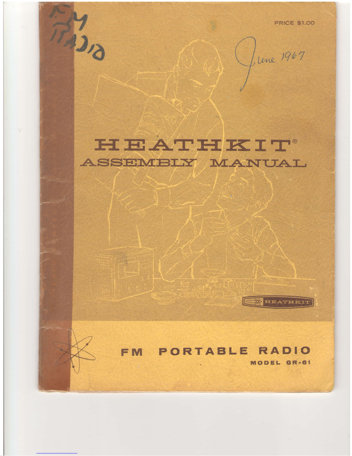
/A.SSE\4E}I-,Y
IAA,NT.IA"I-
H-TA..TH-<IT=
FM
PORTABLE
RADIO
MODEL
GR.6I
tii
Page 2
4
{
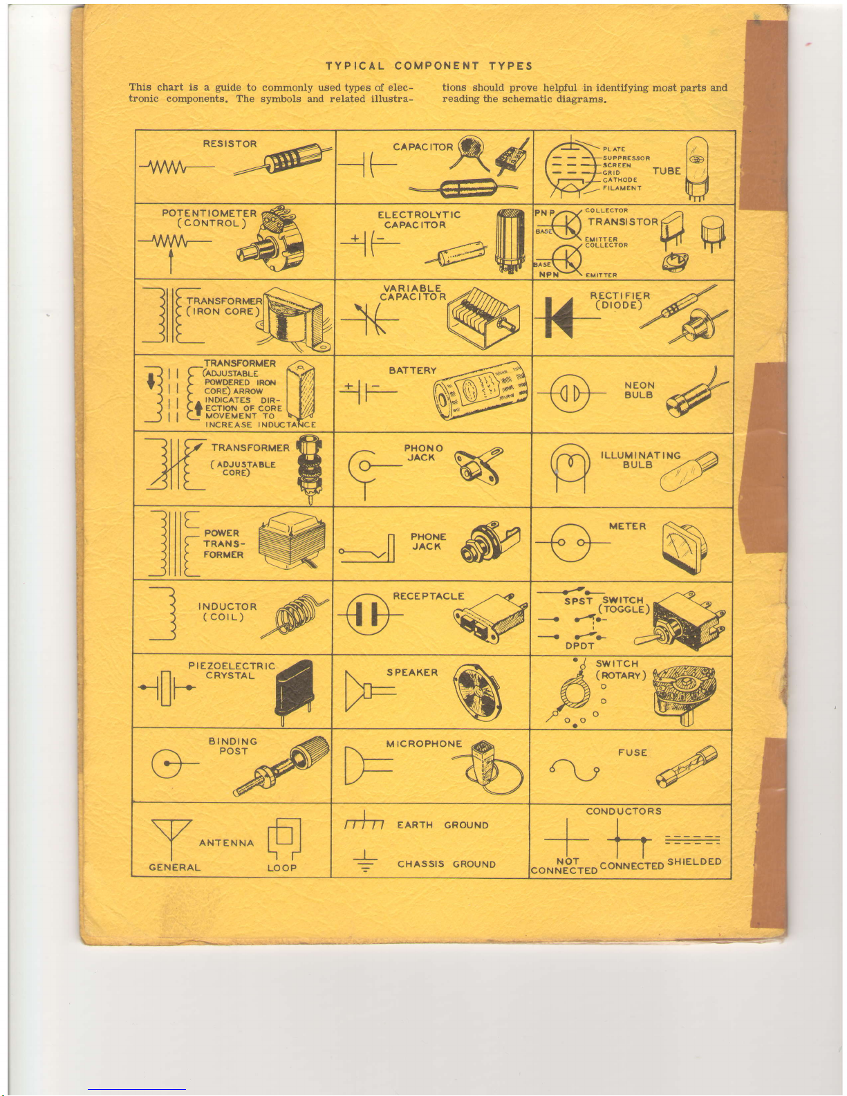
TYPICAL
COMPONENT TYPES
This
chart
is a
guide
to commonly used types
of
elec- tions should
prove
helpful in identifying
most
parts
and
tronic
components. The symbols and
related illustra-
reading the
schematic diagrams.
i
I
RESISTOR
aAA/v!-
ffi
;l^"o"'-o"Rr@
PLATE
SUPPRE$OR
lilo'*
ruBE
CATHOOE
F
ILAM EN T
POTENTIOMETER
(
coNrRoL
)
c
ELECTROLYTIC
CAPACITOR
+ll-
-lt--
COLLECTOR
TRANSISTOR
EMITT ER
COLLECTOR
EM ITTER
m
f-lpaxsroRuER
f'..'o"'|
RECTIFIER
(DloDE)
c-emi":,l3PER <>
!
PoWDERED
rnol
I V1',J
!
cone)
ennow
I li' .',t
Lrh'i^H'$*nM
BATTERY
I
l-
NEON
EULB
I !Z
rnr*sroRMER
||t_,^,**t**.
PHONO
(r'o"^
Y
'ttx,Jl|''ffi
lf
l_
PowER
| >
TRANS-
lL
FoRMER
PHONE
JACK
O--.,,
I
NDUCTOR
(colL)
RECEPTACLE
q
--{>
sPsT
.swlrcH
-
(
TOGGLE
)
€
/l;
--{
}r-
DPDT
nlF''39!+fI^'fl
S
PEAKER
'd swrTcH
A4(n'o
'7
U"
o o
BINDING
POST
t
M ICROPHONE
FUSE
ANTEN
NA
GENERAL
LOOP
I
ITTTT
I
EARTH GROUND
CHASSIS GROUND
CONOUCTORS
Page 3
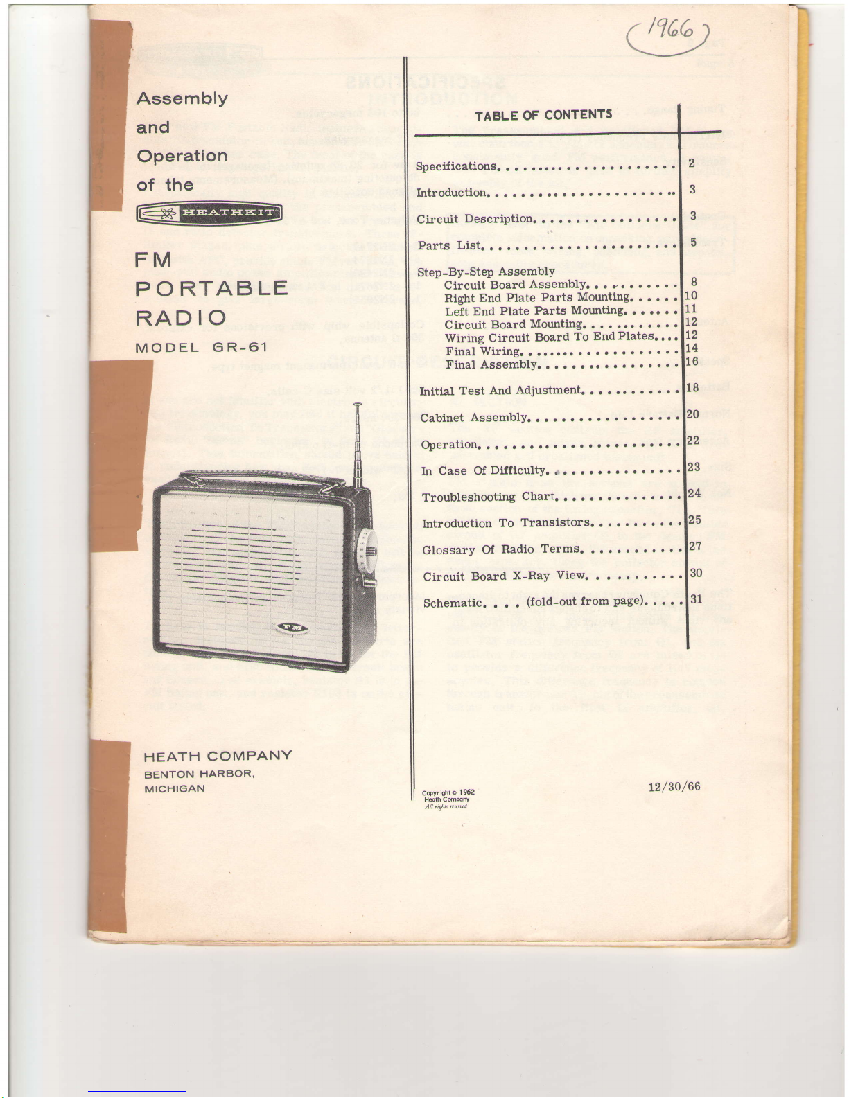
Assembly
and
Operation
of the
FM
P O
RTAB
LE
RAD
IO
MODEL
GR-61
'===*=,
HEATH
COMPANY
BENTON
HARBOR,
MICHIGAN
TABLE
OF
CONTENTS
Specifications.
. .
.
Introduetion.
Circuit
Description.
Parts
List.
Step-By-Step
AssemblY
Circuit
Board
AssemblY.
.
.
Right
End
Plate
Parts
Mounting.
Left End
Plate
Parts
Mounting.
Circuit
Board
Mounting.
. .
Wiring Circuit
Board
To
End
Plates.
.
..
Final
Wiring
Final Assembly.
.
.
Initial
Test
And
Adjustment.
. .
Cabinet
AssemblY.
Operation.
In
Case
Of
DifficultY
Troubleshooting
Chart.
Introduction
To
Transistors.
.
.
Glossary
Of
Radio
Terms.
Circuit
Board
X-RaY
View.
(fold-out
from
Page).
.
. .
.
Cqyrlghto
t962
12/3O/66
2
3
3
D
30
31
Page 4
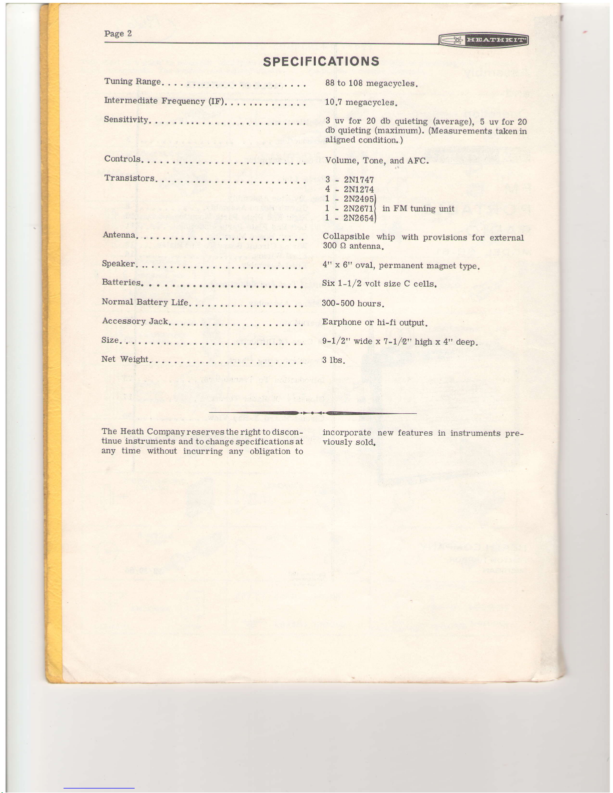
SPECIFICATIONS
Tuning
Range.
Intermediate
Frequency (IF').
. .
Sensitivity.
Controls.
Transistors.
Antenna.
Speaker.
Batteries.
Normal
Battery
Life.
.
Accessory
Jack.
.
Size.
.
Net
Weight.
The Heath
Company
reserves the
right
to discon-
tinue
instruments
and to
change specifications
at
any
time
without
incurring any
obligation
to
88 to
108 megacycles.
10.7
megacycles.
3
uv for
20 db
quieting
(average),
5 uv for 20
db
quieting (maximum).
(Measurements
takenin
aligned
condition.
)
Volume,
Tone,
and AFC.
3
-
2N174?
4
-
2Nt274
1
-
2N24e5l
1
-
2N26711
in FM
tuning
unit
1
-
2N26541
Collapsible
whip
with
provisions
for
external
300 Q
antenna.
4r x
6t'
oval,
permanent
magnet
type.
Six l-l/2
volt
size
C
cells.
300-500
hours.
Earphone
or
hi-fi
output.
9-L12"
wide x 1-l/Q,,high
x 4"
deep.
3 lbs.
incorporate
new features
in instruments
pre-
viously
sold.
I
*
)
Page 5
_--I
l@l
n*"g
INTRODUCTION
Your
new
FM Portable
Radio
featuresadepend-
able
10-transistor
circuit,
housed
in
an attractive
imitation-leather
case.
The
front
of
the
case is
made
of durable
high-impact plastic.
Exceptionally
high
quality
is designed
into
this
Radio,
as
evideneed
by ttre
preassembled
and
prealigned
FM
tuning
unit, and
the
prealigned
IF
and
ratio
detector
transformers.
-ThreJIF-
limiter
stages,
plus
a ratio
detector
combina-
tion
with
AFC, provide
stable
FM
reception. The
push-pull
audio
power
amplifier
circuit delivers
more
than
adequate power
for the
4" x
6"
speaker
to give
large-room
sound
coverage.
CIRCUIT
DESCRIPTION
The
preassembled
and
prealigned
FM tuning
unit contributes
to
ease
of
assemblyandinsures
consistently
good
FM
performance.
A
heavy-
duty
circuit
board
is used
to further
simplify
assembly
of
the
kit.
If
you
are not
familiar
wlth
electronic
circuitrv
and
terminology,
you
may
find it helpful to
reai
the
I'Introduction
To
Transigtorsr
and
"Glossary
Of
Radio
Terms"
beginning
on
Page
2?
of
ttre
manual.
This
information
should
prove
helpful
in
understanding
how
your
Radioworkswhenyou
read
the
following
Circuit
Description.
The
circuitry
of the FM
Portable
Radioconsisrs
of
the
RF, IF-limiter,
ratio detector,
and
audio
sections.
For
simplicity,
each
section will
be
discussed
separately,
Refer
occasionally
to the
Schematic
Diagram
while
reading
tris
descrip-
tion.
To
help
in
reading
the
Schematic,
the
letter-
number
designations
for
t}e
circuit
parts
are
number
coded
as follows: #1
to
gg
for the FM
tuning
unit, and
#100 to
200 forthecircuit
board
and
chassis.
For
example,
resistor
R3 ig in the
FM
tuing
unit, and
resistor
R,103
is
onthe cir-
cuit
board.
NOTE:
Refer
to
the
"Kit
Builders
Guide"
for
complete
information
on unpacking,
parts
identi-
fieation,
tools,
wiring,
soldering, and
step-by-
e
RF
SECTION
The
RF
section
contains
the
RF amplifier,
oscillator,
and
mixer
stages,
all
in
i
pre-
assembled
and
prealigned
tuning
unit.
FM
signals
from
the
antenna
are applied
to
transformer
T1
,
which
matches
the
antenna
to the
first
section
of
the tuning
capacitor,
C1A. This
portion
of
the
tuning
capacitor tunes
ttre
emitter
circuit
of RF
amptifier
Ql
to the
desired
FM
station
frequency.
C1B,
the
second
section
of
tlte
tuning
capacitor,
tunes
the
collector circuit
of
Q1
to the
same
station
frequency.
Q2
is
operated as
a feedback
tuned-collector
oscillator at
10.?
megacycles
above the
fre-
quency
of
the
desired
FM
station. The
ampli-
fied
FM
station frequency
from
Q1,
and the
oscillator frequency
from
Q2
are mixed
in
Q3
to
provide
a
difference
frequency
of
10.7
meg-
acycles. This
difference
frequency
is coupled
tirough
transf
orme r T2,
out
of
the
preas
se mble d
tuning
unit,
to the
first IF
amplifier,
Q4.
I
t
I
l
I
I
1
-l
I
{
Page 6
n"u"a
@EGBI
The circuit of
the
P.E.C.
includes
a
de-empha-
sis
network
to
compensate
for high
frequency
pre-emphasis
that was
added to
the transmitted
audio
signal;
it thus
provides
a
flat audio
fre-
quency
response.
This network
also attenuates
frequencies
above
the audio range.
The audio
output
signal
of
the ratio
detector is
applied
both
to
Q7,
the
emitter
follower
and, as
an
AFC
voltage,
to
Q2
oftheFMtuning
unit.
Any
shift of
the
IF from
the
10.7
megacycle
center
frequency
appears
as
a DC voltage
which
is ap-
plied
to
diode D1;
this is
commonly
called
AFC
voltage.
The
DC
voltage
shift on
D1 in
turn
changes
the oscillator
capacity,
thereby ef-
fectively retuning
it and causing
it to
track the
particular
station
that is
being
received.
AUDIO
SECTION
The audio signal
from
the ratio
detector is
applied to
Q7,
the emitter
follower,
which acts
as
a matching networkbetween
the
ratio
detector
and
the Volume control.
After
the Volume control,
the audio signal
is amplified
bydriver
amplifier
Q8
and
then
to the
Tone
control
and
to driver
transformer
T6. Transformer
T6
couples
the
audio signal
to
Q9
ahd
Q10,
ttte
push-pull
audio
amplifier stages.
From
Qg
and
Q10
the signal,
is coupled
to the speaker
and
earphone
jack
through
T?,
the audio output
transformer.
When
an
earphone is
plugged
in,
the built-in
speaker
is automatically
disconnected
from
the
circuit
and
the
audio signal
goes
instead
to the ear-
phone.
Operating
power
is supplied
by six
1-1/2
volts
size
C
flashlight
batteries.
IF-LIMITER
SECTION
The
10.?
megacycle signal
from
the
FM tuning
unit is
appliedto
Q4,
the
first IF amplifier.
From
Q4,
the
IF signal
passes
through
transformer
T3'
which
passes
only
the difference
frequency
of 10.?
megacycles,
to
Q5,
the
second
IF amplifier.
After
additional amplification
in
Q5,
the signal
is
applied
through T4, the second
IF transformer,
to
limiter stage
Q6,
which limits on
all but
the
weakest
signals.
Stages
Q4
and
Qb
act as
IF amplifiers
for
weak
signals,
and
as limiters
for
strong
signals.
Limiter
stages
are used
to remove
any
AM
(amplitude
modulation)
of
the IF signal,
and
to
limit
the signal
to
the
proper
level
for
the ratio
detector.
The IF signal
from
limiter
Q6
is next
applied
to ratio
detector transformer,
T5.
RATIO DETECTOR
Ideally,
the IF
signal
applied
to
the ratio
de-
tector should be of constant
amplitude,
but con-
tain
variations
in frequency
which
correspond
to
tfie audio signal being
transmitted
by
the
FM
station.
The
amount of
frequency
deviationfrom
the center
frequency of
10.7
megacycles
de-
termines
the amplitude of
the resulting
audio
signal.
The number of
times
per
second
thatthe
IF
signal
deviates from 10.?
megacycles
de-
termines
the resulting
audio
frequency.
The
combinatlon of
diodes D3, D4, and
transformer
Tb detect frequency variations
in the
IF
signal,
and
change
these variations
into
anaudiosignal.
Most of
the resistors
and capacitors
used
inthe
ratio
detector
are encapsulated
in a
P.E.C.
(pack-
aged electronic
circuit).
The
use of
this
P.E.C.
eliminates
any variations
in
performance
that
could
result
from
different
wiring
techniques.
Page 7
@EE@l
P"e"s
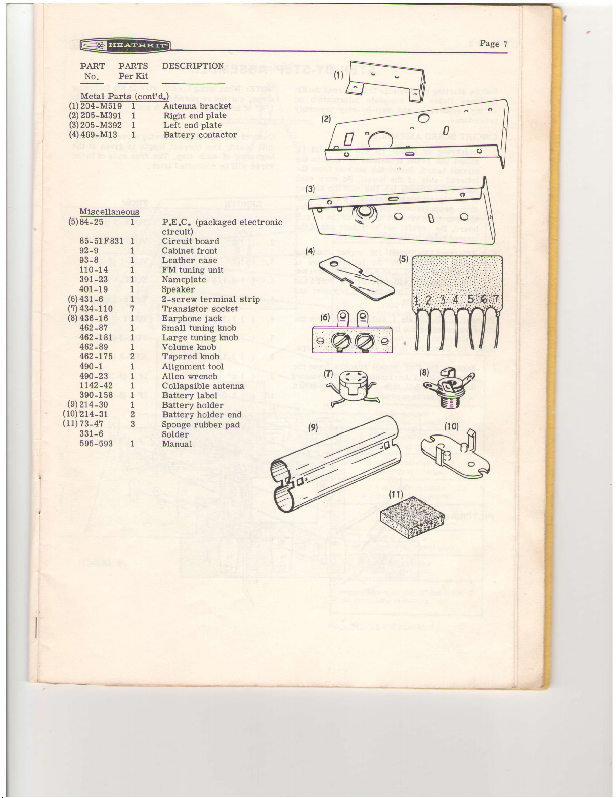
PARTS
LIST
The
numbers in
parentheses
in the Parts List
are keyed
to the
numbers in the Parts drawings
to aid in
parts
identification.
PART
No.
PARTS
Per
Kit
DESCRIPTION
4.7
Q
(yellow-violet-gold)
10 Q
(brown-black-black)
68 A
@Iue-gray-black)
220 Q
(red-red-brown)
820 A
(gray-red-brown)
1
KO
(brown-black-red)
1.2
KO
(brown-red-red)
2.?
KO
(red-violet-red)
3.3 KO
(orange-orange-red)
4.1 KA
(yellow-violet-red)
6.8 Kft
(blue-gray-red)
10 KO
(brov'n-black-
orange)
t2 KQ
(brown'red-orange)
15 KO
(brown-green-orange)
18
KO
(brown-gray-orange)
22 KA
(red-red-orange)
68
Kf)
(blue-gray-orange)
1 00 KO
(brown-
black-
yellow)
1 megohm
(brown-black-
green)
PART
PARTS
No.
Per
Kit
Controls-Switch
(5)
10138- 1-
"
(6)
1e-81
(?)
60-18 1
Choke-
Transf
ormers-
Diode
DESCRIPTION
100
KO linear
control
10 KQ
control
with SPST
switch
SPST
switch
Resistors
(1)
1:T20
t-4L
L-2
t-45
1-8
1-9
1-
10
1-
13
t-r4
1- 16
1- 19
L-20
1-109
L-21
1-69
t-22
1-60
r-26
1-
35
Capacitors
(2)2
-
2t-46
2t-94
(3)
25-54
(4)
25- 11 5
25-116
25-tl?
25-11 1
(8)
45-35
(e)
sr-sz
51-98
(10)
52-57
53-6
(11)
56-26
(81
(10)
2
1
1
2
1
I
1.?
ph
choke
Driver transformer
Output
transformer
IF transformer
Ratio detector transformer
Crvstal
diode
1
I
I
1
4
I
2
1
210
ttttf
disc
ceramic
.005
pfd
disc ceramic
.05
pfd
disc
ceramic
10
pfd
15
V tubular
electro-
lytic
10
pfd
15
V
electrolytic
50
pfd
15
V
electrolytic
100
pfd
15
V
electrolytic
1000
pfd
15
V tubular elec-
trolytic
tzt
1-7
\\=t-
/-
{4r lf-----------v
l-
^r--
J"
'::-
Page 8
a
{
n'u"u
@EEFI
PART
No.
PARTS DESCRIPTION
Per
Kit
PART
No.
PARTS
DESCRIPTION
Per
Kit
Transistors
4t7
-10
1
411
-7t
1
411
-72
1
411
-57
3
tt7-2
1
2N2671
transistor
tuning
unit)
2N2654 transistor
tuning
unit)
2N2495 transistor
tuning
unit)
2Nl74? transistor
Transistor
package
contain-
ing four
part
no.417-21,
type
2N1214 transistors
3-48
x 1/4" screw
4-40
x
1/8" setscrew
6-32
x 3/16" screw
6-32
x l/4" screw,
phillips
head
6-32 x L/4"
sctew, binder
head
6-32
x
3/8"
screw
6-32
x
3/8"
self-tapping
screw
6-32 x l/2"
screw
(in
(in
(in
Hardware
(cont?d.
FM
(18)
254-?
I
(1e)
254-e
2
FM
(20)
254-1 1
(2r)
254-14 2
FM
(22)254-4
1
#3
lockwasher
#4 lockwasher
#6 lockwasher
Small
control lockwasher
Large
control
lockwasher
i
t-
t
I
!
I
Hardware
(1)
250-4e
(2)
250-156
(3)
250-138
(4)
250-22s
(5)
250-56
(6)
250-8e
(?)
250-106
(8)
250-10
343-?
344-50
344-1
6
344-t5
346-1
[
]
${ilrlr
(2)
fo
(3}
frfril
ro
flinm
,rr,-rz+rQ2
,-,F
(16)@
e7l
I
^
(5)
^
(61
^
(71
,
(8)
fl,',ii',',i
l,p,i,'*rr
gF**
t}.**t
I
2
8
3
d
2
n
4
@
@
4
2
1
1
2
4
10
4
2
wire
wire
wire
(s)
252-r
(10)
252-15
(11)
252-3
(L2)
252-22
3-48
nut
4-40
nut
6-32
nut
6-32
speednut
(ls)
@
(16)
(l
z1
@
g
(r
a1
(l
e)
(20)
(21
)
ezl
@@@@@
.
r3)
255-11
(24)
25e-rt
(25)
25e-12
(26)
455-31
(2?)
258-30
Metal Parts
(Zg)
tOO-rr,rarO
r
(2e)
1oo-M41?
1
(30)
zo4-Mb1?
1
Cable-Wire-SleevinE
Tapped
spacer
Spade
lug
Large
solder lug
Antenna
bushing
Battery
spring
Length
shielded cable
Length
black hookup
Length
stranded
red
Length
stranded black
Length sleeving
Switch
lever
Bottom
circuit board
bracket
Top
circuit board bracket
ota:lno)g rlr).
urt&
Small control
nut
Large control
nut
Flat
washer
Thin
nylon shoulder
washer
Thick nylon
shoulder
washer
(13)
(14)
(13)
252-3e
(r4)
252-7
(15)
253-45
(16)
?5-18
(1?)
2b3-Eo
3
1
2
1
I
Page 9
r*
Page
T
PART
No.
PARTS
DESCRIPTION
Per
Kit
Metal Parts
(cont'd.)
(1)
mA:IFI0--T------Tntenna bracket
(2)
205-M391
(3)
205-M392
(4)
46e-Ml3
85-51F831
92-9
93-8
110-14
391
-23
401-19
(6)
431
-6
(?)
434-110
(8)
436-16
462-81
462-r8r
462-89
462-175
490-1
490
-2
3
tr42-42
390
-1
58
(e)
214-30
(10)
i214-31
(1
1)
?3-4?
331
-6
595-593
Right
end
plate
Left end
plate
Batterv contactor
1
1
1
I
I
1
1
I
1
1
1
7
I
1
I
1
2
1
1
1
1
1
2
3
1
P.E.C.
(packaged
electronic
circuit)
Circuit
board
Cabinet
front
Leather
case
FM tuning
unit
Nameplate
Spealer
2-screw terminal strip
Transistor
socket
Earphone
jack
Small tuning larob
Large tunlng knob
Volume
knob
Tapered knob
Alignment tool
Allen
wrench
Collapsible
antenna
Battery
label
Battery
holder
Battery
holder end
Sponge
rubber
pad
Solder
Manual
,?"€r
\-----
Page 10
_.-TOP
SIDE
,f
NOTE:
SOCKETS MUST
@@
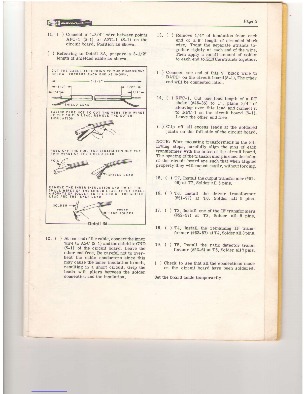
11.
(
)
Conn
AFC.
circr
(
)
Referring
length
of
CUT
THE
CAE
BELOW.
PRE
TAKING CAR€
OF
THE
SHIEI
INSULATION.
PEEL OFF
TI'
THIN WIRES
(
Defoi
Detoil
lA
dj,
BE INSERTED FROM
THE TOP
(LETTERED}
SIDE
OF THE CIRCUIT
BOARD.
THIS IS
THE
SIDE
OPPOSITE THE
METALIC FOIL.
,,1,::
ir
REMOVE
THE
SMALL
IYIRES
AMOUNTS
OF
LEAD
ANO
TH
SOLDER
--{
v
L2.
(
)
Ator
w'ire
(s-1)
othe:
heat
may
resu
leadr
conn
KEYWAY
Page 11
ttB
Detqil
lC
.:1::
t1.r
;::1i
Page
8
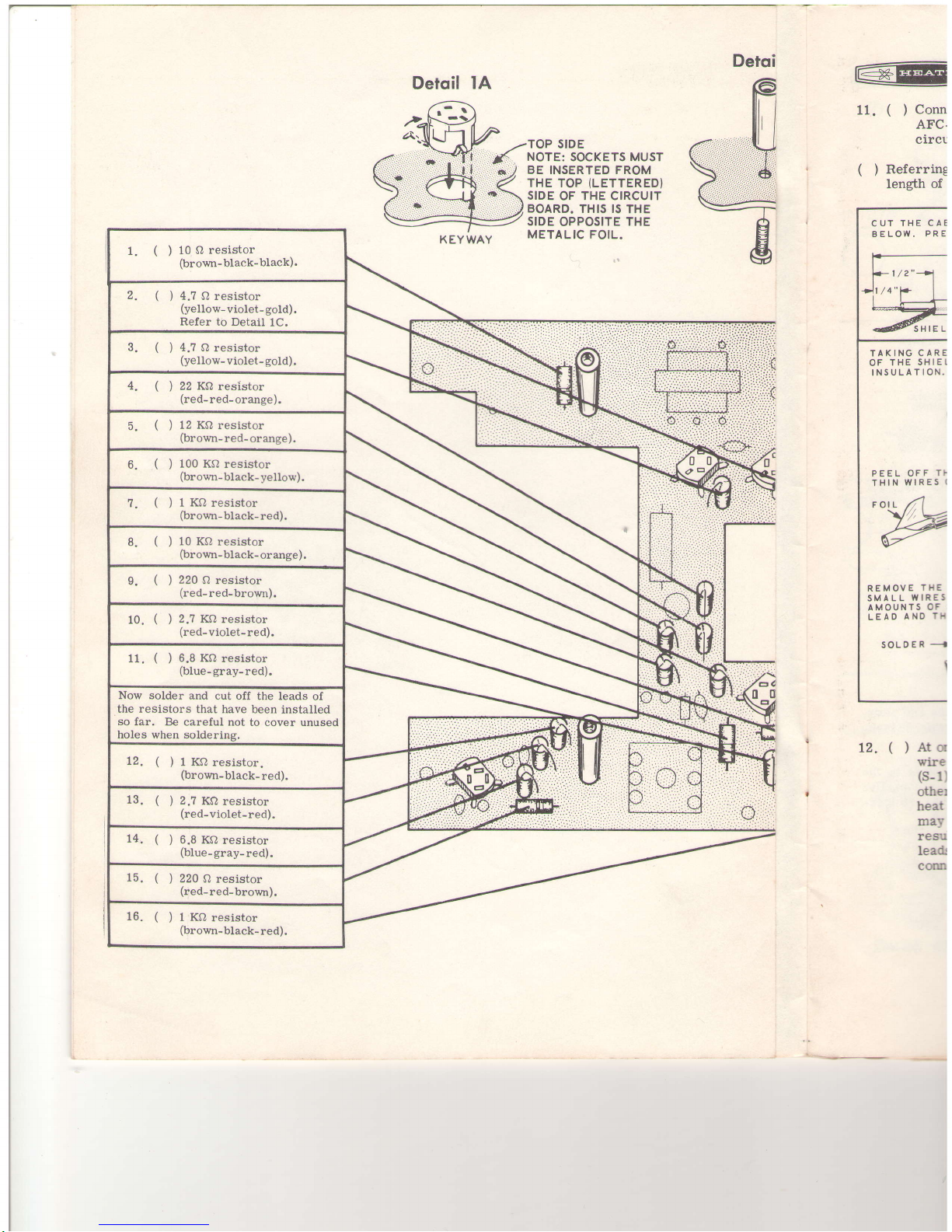
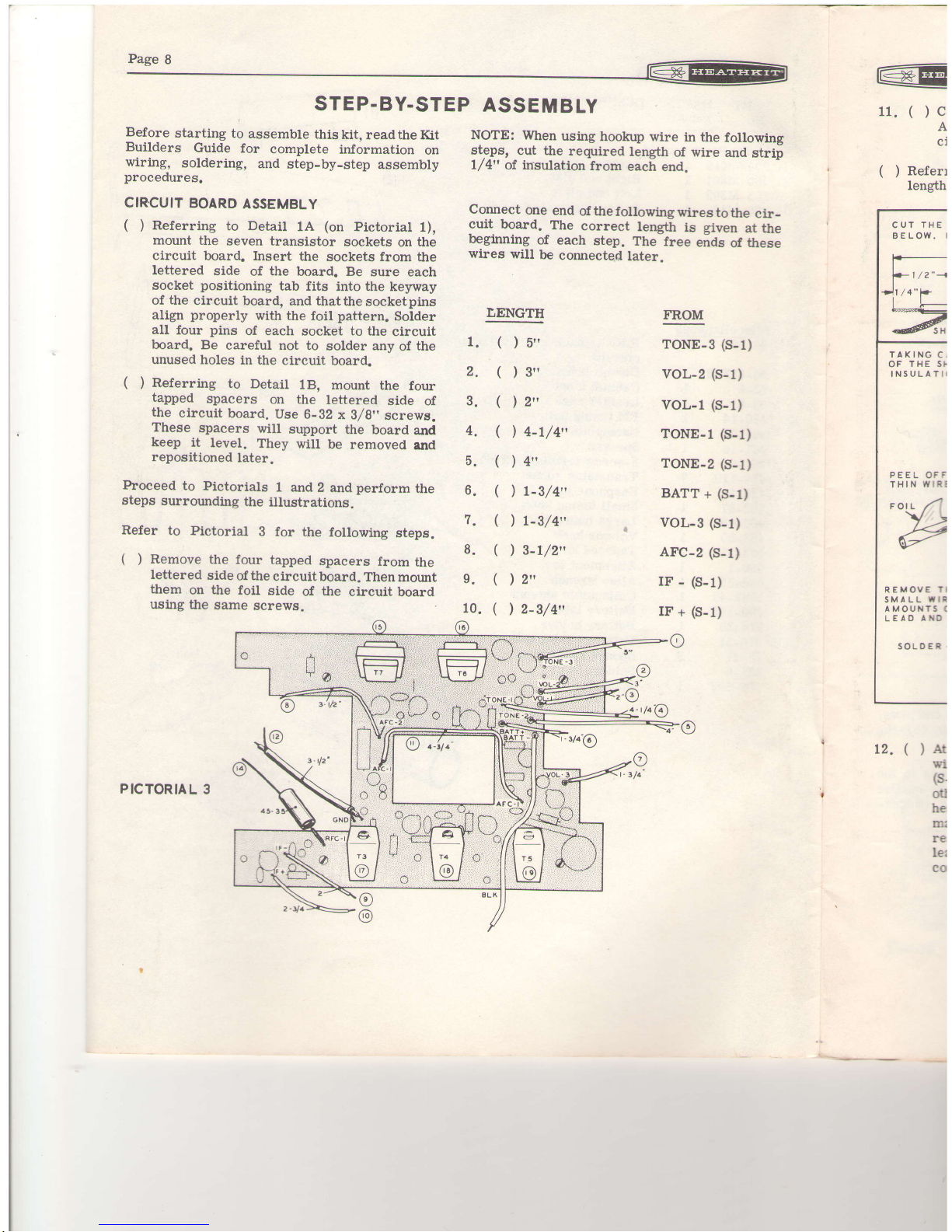
Before starting
Builders
Guide
wiring,
solderit
procedures.
CIRCUIT
BOARI
(
)
Referring
t
mount
the I
circuit
boal
lettered
si<
socket
Posi
of
the
circu
align
ProPe
all
four
Pir
lrcard.
Be
r
unused
hole
(
)
Referring
tapped spa
the
circuit
These
spac
keep
it le'
rePositione
Proceed
to
Pic
steps
surroundi
Refer
to
Picto
(
)
Remove
th
lettered
sit
them on
th
using
tlte s
PICTORIAL
3
PICTORIAI
I
PROCEED
TO
PICTORIAL
2
Page 12
STEP.BY.STEP
ASSEMBLY
|@E
11.
(
)c
A
ni
Before
starting
to
assemble
this
kit,
readthe Kit
Builders
Guide
for
complete
information
on
wiring,
soldering,
and
step-by-step
assembly
procedures.
CIRCUIT
BOARD
ASSEMBLY
(
)
Referring
to
Detail
1.{
(on
Pictorial
1),
mount
the
seven transistor
sockets
on
the
circuit
troard. Insert
the
sockets from
the
lettered
side
of
the
board. Be
sure each
socket
positioning
tab fits
into the keyway
of
the
circuit
board, and thatthe
socketpins
align
properly
with
the foil
pattern.
Solder
all
four
pins
of
each socket to the
circuit
board.
Be
careful not to
solder
any
of
the
unused holes
in the
circuit
board.
(
)
Referring
to
Detail
18, mount
the
four
tapped
spacers
on
the
lettered
side of
the
circuit
board.
Use
6-32
xg/g,,screws.
These
spacers
will
support
the
board
and
keep
it
level.
They
will
be
removed
and
repositioned
later.
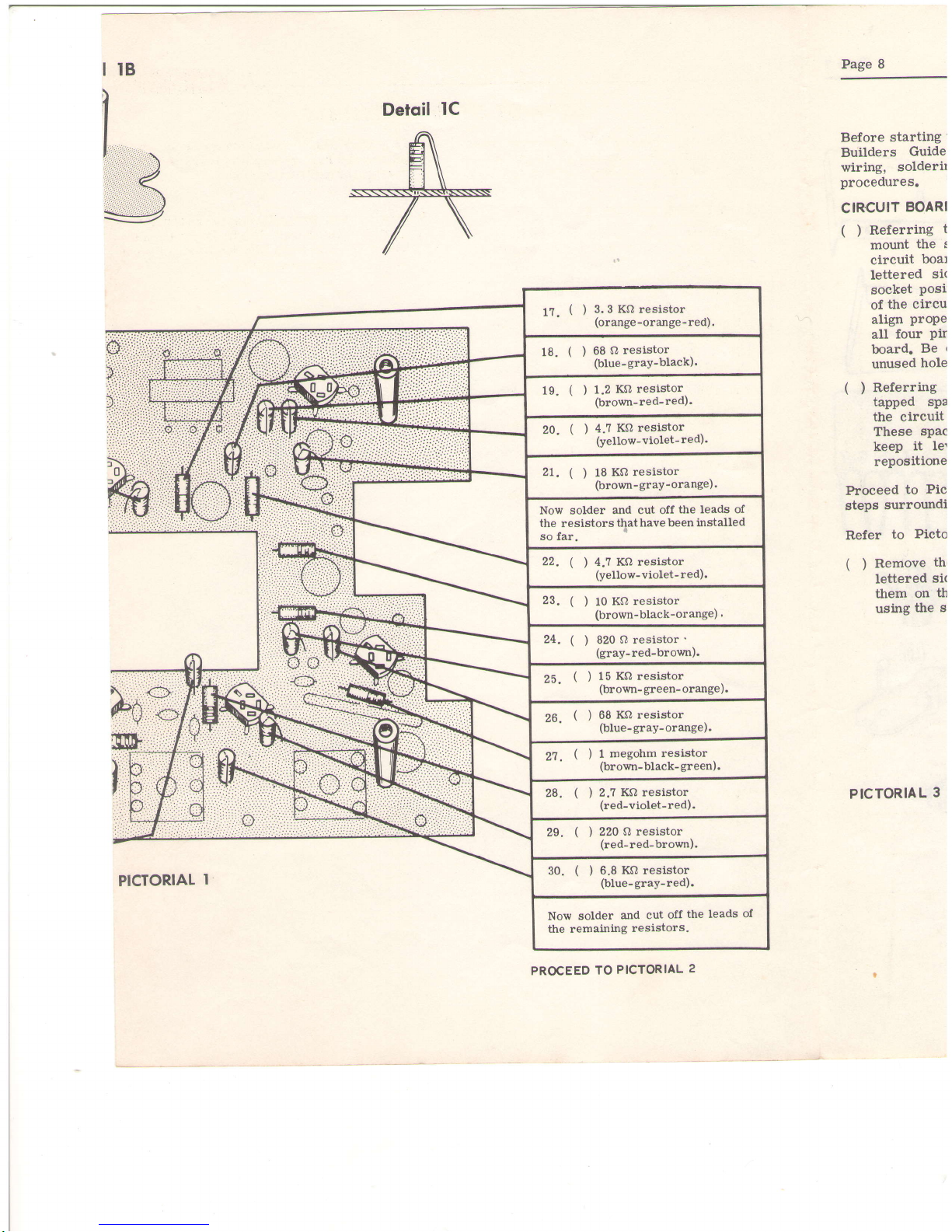
Froceed
to
Pictorials
1 and
2 and
perform
the
steps
surrounding
the
illustrations.
Refer
to Pictorial
3
for the
following
steps.
(
)
Remove
the
four
tapped
spacers
from
the
lettered
side
of the
circuit board.
Then
mount
them
on
the
foil
side
of
the
circuit
board
using tlle
game
screws.
PICTORIAL
3
NOTE:
When
using
hookup
wire
in the
following
steps,
cut the
required
length
of
wire
and
strip
l/4
of. insulation
from
each end.
Connect
one
end
of thefollowingwirestottre
eir_
cuit board.
The
correct
length
is
given
at the
beginning
of each
step.
The
free
ends
of
tlese
wires
will
be
connected
later.
1.
(
2.(
3.(
4.(
5.(
6.(
t.
\
8.(
e.(
10.
(
)5"
)3"
)2"
)
4-t/4"
)4"
)
r-3/4,'
I
L-3/4"
)
3-r/2,,
)2"
)
2-3/4"
LENGTH
FROM
TONE-3
(S-1)
vol-z
(s-1)
vol-1
(s-l)
TONE-1 (S-1)
TONE-2 (S_1)
BATT
+
(S-1)
vol-3
(s_1)
AFC-z (S-1)
rF
-
(s-1)
IF
+
(S-1)
(
)
Referr
Iength
CUT
THE
BELOW. I
TAKING
C,
OF
THE SF
INSULATII
PEEL
OFF
THIN
WIRI
REMOVE
TI
SMALL
WIF
AMOUNTS
(
L
E A D A
ND
SOLDER
12.()
At
w'i
(s.
ou
he
mi
re
lei
co
F-+::i
l
/_---"1
\-f",
\l= JJ
\n*}n
\\./
oi^./
ilVffi
LJ^II
&J
ra/
vt
Page 13
I@EEEEEEFI
nu*"
n
11.
(
)
Connect
a 4-3f4,'
wire
between
points
AFC-1
(S-1)
to
AFC-I
(S-1)
on
tne
circuit
board.
Position
as
shown.
(
)
Referring
to Detail
3A,
prepare
a
J-t/Z',
length
of shielded
cable as
shown.
12.
( ')
At
oneendofthecable.connecttheinner
wire to AGC
(S-1)
andtheshieldtoGND
(S-1)
of
the
circuit
board. Leave
tlre
other end free.
Be
careful not to
over-
heat the
cable
conductors
since this
may
cause the
inner
insulation to
melt,
resulting
in
a short
circuit.
Grip the
leads
with
pliers
between
the
solder
connection
and the
insulation.
13.
(
)
Remove
l/4t' of insulation from
each
end
of a
9" Iength
of
stranded black
wire.
Twist
the
separate
strands
to-
gether
tightly
at each
end
of
the
wire.
Then
apply
a
small amount
of
solder
to
each
end toh6iTifre
strands
tosether.
(
)
Connect
one end
of
this
g"
black
wire
to
BATT-
on
the
circuit
board
(S-1).
The
other
end
will
be
connected
later.
14.
(
)
RFC-1.
Cut
one lead
length
of a RF
choke
(#45-3b)
to
1",
place
B/4,'
of.
sleeving
over this
lead
and
connect it
to
RFC-I
on
the
circuit
board
(S_1).
Leave
the
other end
free.
(
)
Ctip
off
all
excess
leads
at the
soldered
joints
on
the
foil
side
of
the
circuit
board.
NOTE:
When
mounting
transformers
in the
fol-
lowing
steps,
carefully
align the
pins
of each
transformer
with the
holes
of
the
circuit
board.
The
spacing
of
the
transformer
pins
and
the
holes
of
the
circuit
board
are
such that
when
alisned
properly
ttrey
will mount
easily,
withoutforJing.
15.()
16.()
1?.()
T7.
Install
the
outputtransformer
(#b1-
98) at T?.
Solder
all
5
pins.
T6. Install
the driver
transformer
(#51-97)
at
T6. Solder
all
5
pins.
T3.
Install
one
of
the
IF transformers
(#52-51)
at
T3.
Solder
all
8
pins.
18,
(
)
T4.
Install the
remaining
IF trans-
former
(#52-51)
at T4. Solder
all 8
pins.
19.
(
)
T5.
Install
the
ratio detector
trans-
former
(#53-6)
at TF. Solder
all?pins.
(
)
Check
to
see
that
all the
connections made
on the
circuit
board have
been
soldered.
Set the
board
aside temporarily.
ll
v
t
l
t
i
:
I
;
I
I
I
I
CUT THE
CABLE
ACCORDING
TO
THE DIMENSIONS
BELOW.
PREPARE
EACH END
A5 SHOIVN.
IAKING
CARE
NOT
TO
CUT THE VERY THIN WIRES
OF THE SHIELD
LEAD,
REMOVE
THE
OUTER
INSULATION.
PEEL
OFF THE
FOIL AND
STRAIGHTEN
OUT
THIN WIRES
OF
THE SHIELO
LEAD.
REMOVE
THE
INNER
INSULATION
AND TIVIST
THE
SMALL
IYIRES
OF THE
SHIELO
LEAD.
APPLY
SMALL
AMOUNTS
OF
SOLDER
TO THE ENO
OF THE SHIELO
LEAO AND
THE
INNER
LEAO.
Page 14

(
)M
b:
th
sl
s(
la
()M
al
p
()M
#i
Set U
LEFT
Refer
(
)M
oo
[-__l,
tl
-r-T
8ru r3z+"
Ao
V
€
fi,
AFC
swtTcH
c
f-l
u
I lAFc-r
tl
tl
r
I te I
\,/
,
r|\
ea
De-
nfc
AGC
NIT
6)
FM
ING
U
@
-t
a
Qz
B(
t-l
c
?
SOLDE
R
LUG
,-l
N
E
2Nt747
Q4
\Yd
'
tF+
N
..+iiii
@)
,lT-l
@
@
k1
Page 15

oo
tl
-t-l-
8ru rZza"
Ao
t\)
{-e
il,
AFC
swlTcH
a
nu
I lAFc-
L_l r)
a)
\__/
|
(r)
o-a
oC-
nf0
AGC
TUN
NIT
6)
FM
ING
U
@
-l
a
€z
B(
t-ic
?
SOLDE R
LUG
lt
c-l
I/ve I
,/
'C+
RF
1__r
N
E
2Nt747
o4
0r-d
'
rF+
N
..,:r;jiil
-.i..:rj:f
4E
@
@
k1
(
)M
br
tt
s1
st
Ia
()M
AJ
p
()M
#1
Set
tl
LEFT
Refer
()M
Page 16

ll
n O
voL-z
o
o
o
YY ,....: L
rooo
llFD
@
NTROL
TONE
CONTROL
Page
10
6-32
SPEEDN
FLAT
SIDE
6-32
NUT-\
LOCKWASH
ER
-
T
ER
MIN/A
RIGHT
END PLA'
Refer
to
Detail
(
)
Mount
two
6-
plate.
Be
surr
is
positioned
NE
o
TO
-3
lNr274
A
L-/€
EQ5
-\n
,-\TONE-lc
r\ Vr(f
I l,'^\ | I
\\_/rfrffi
BATT_
f]
-i-
\7-
O
O
O
a1
OLJ
2N1747
A
())C
BGF
Y
:fJ
Deloil
1F
PICTORIAT
Page 17

6-32
X3lt6"scREW
6-32
SPEEDNUT
AFC
SWITCH
*T
6
LOCKWASHER
6-32
NUT
THIN
NYLON
SHOULOER
WASHER
AN
TE
NNA
BUSHING
SOLDER
SMALL
CONTROL
T
HICK
NYLON
SHOULDER
WASHER
RIGHT
END PLATE
PARTS
I,IOUNTING
Refer
to Detail
44,
for
tfie
following
steps.
(
)
Mount
two
6-32 qreeftruts
on
&re
right
end
plate.
Be
sure ttre
flat
side
ofeachspeednut
is
positioned
as
shown.
Detdil
4A
Mount
the
antenna
bracket
to the
end
plate.
Use
6-32
x 1/4"binder
head
screws,
#6
lock_
washers,
and
6-32
nuts.
Mount
the
2-screw
terminal
strip to
the
antenna
bracket.
Position
it
as
shown.
Use
6-32
x
1/4"
binder
head
screws.
#6
lock_
washers,
and
6-32
nuts.
()
()
(
)Mc
bri
thi
slr
sol
lar
(
)Mc
an(
pol
()Mc
#6
Set
thr
LEFT E
Refer
(
)Mo
RIGHT
END PLATE
6
-32X1/4'
B
IN
OER
/^(t\
v
i
VorurEN*e
BRAC
KET
TERMINAL
STRIP
6-32xt/4
BTNDER
HEAD
SCREW
Page 18

@EE@l
Pagell
TROL
NUT
CONTROL
NUT
LEFT
ENO PLATE
LARGE
CONTROL
LOCKWASHER
VOLUME
CONTFIOL
Detqil
48
EAFIPHONE
,O.**ffi
TONE
CONTROL
(
)
Mount
the
antenna
brtrshing
to
the
antenna
bracket.
Use the
thicknylon
shoulder
washer,
thin
nylon
shoulder
washer,
solder
lug, and'
small
control
nut.
position
and
ben-d the
solder
lug as
shown.
Tighten
securely
with a
Iarge
screwdriver.
(
)
Mount
the
AFC
switch
with
#4 lockwashers
and
4-40
nuts.
Be
sure the
switch
lugs are
positioned
as
shown.
See
pictorial
4.
(
)
Mount
the
preassembled
FMtuningunitwith
#6 lockwashers
and
6-82
x
B/16n
screws.
Set
the
right
end
plate
aside temporarily.
LEFT
END PLATE
PARTS
MOUNTING
Refer
to Detail
48
for the
following
parts.
(
)
Mount
two
6-32
speednuts
on
the
left end
plate.
Be
sure the
flat
side
ofeachspeednut
is
positioned
as
shown.
(
)
Mount
the
Volume
control
(#19-g1)
with
a
large
control
lockwasher
and
large
control
nut.
Position
th€
lugs
as
shown.
(
)
Mount
the
Tone
control
(#10-1gg)
with
a
small
control
lockwasher
and
small
control
nut.
Position
the
lugs
as
shown.
(
)
Mount
the
earphone
jack
with
a
small
con-
trol
loekwasher
and
small
control
nur.
Position
the
lugs as
shown.
Set the
left
end
plate
aside temporarily.
Page 19

CIRCUIT
BOARD
MOUNTING
Page
12
Refer
to
Detail
4C
for the
following
steps.
(
)
Prethread
the
endholes
ofthetopahdbottom
circuit
board
brackets
with
a-O-gZ
xg/g,,
self-tapping
screw.
(
)
Mount
the
eircuit
board
to
the
tqp
and
bottom
brackets.
Use
B-49
x
L/4,,
screws.
#3
lock_
washers,
and
B-4g
nuts.
Do
not tighten
the
serews.
(
)
Re^ferring
to Detail
4D,
mount
the
right
and
left
endplates
to the
top
and
bottorn
brickets.
Use
6-32
x
3/16"
screws.
position
the
screws
to
the
rear
(away
from
the
flange)
of
the
slotted
holes
in the
end
plates
ind
tighten.
Now
tighten
the
sereu/sthatholdthe
circuit
board
to
the
top
and
bottom
brackets.
WIRING
CIRGUIT
BOARD
TO
END
PLATES
Refer
to Pictorial
4
(fotd_out
trom
nage
tO)
for
the
following
steps.
Conhect
the
free
endg
of the
wires
comins from
the
circuit
board
to
end
plate
terminils
as
directed
in the
folloWlng
steps:
(
)
Connect
a
.05
pfd
digc
ceramic
capacitor
from
lug
4
(S-2)
to
lug
1
(S-2)-
of
the
Volume
control.
FROM
CIRCUIT
BOARD
POINT
(
)
eart+
(
)
TONE-2
(
)
vol,-l
(
)
vol,_z
(
)
roNE-l'
(
)
roNE-3
(
)
vor,-s
(
)
Arc-2
(
)tr-
(
)rr+
TO
lug
4
of
Volume
eontrol
(NS).
Itig
2
of Tone
control
(S-1).
lug
1
of Volume
control
(NS).
lug
2
of Volurne
control
(S.1).
lug
1 of
Tone
control
(S-1).
lug
3
of Tone
control
(S-1).
lug
3
of
Volume
control
(S_l).
lug
2
of AFC
switch
(NS).
IF-
of
FM
tuning
unit
(S-1).
IF+
of
FM
tuning
unit
(S-1).
3-46
x thil
scREw
Detoll
4c
Page 20

i
1
l
I
6-32x
3,/t6rscREW
COMPONENT
SI
DE
{
(
)
at
the
free
end
of
the
shieldedcablecoming
from
the
circuit
board,
connect
the
inner
conductor
to
AGC (S-f)
anO
the
shield
to
GND
(S-1)
of the
FM
tuning
unit.
Grip
the
inner
conductor
and
shield
between
the
insulation
and
the
solder
connection
with
long-nose
pliers
to
prevent
heat
damage
to
the
insulation.
(
)
Connect
the
free
lead
of
choke
RFC-1
to
AFC-1
of the
FM
tuning
unit
(NS).
Use
sleeving.
(
)
Connect
a
Bil
wire
from
AFC_2
on
the
FM
tuning
unit (S-f
)
to
lug
2
of ttre
AfC
s*ii"r,
(s-2).
(
)
Connect
a
3-L/4,,
wire
from
AFC_1
of the
rM
luqing
unit
(S-2)
to
lug
1
of the
AFC
switch
(S-1).
NOJ|
: Where
a
wire
goes
through
a
connection
ancl
men
goes
to
another
point,
as
in
the
next
step,
it
will
count
as
two
wires
inthe
solder
in_
.i15t1ctio1q
(S-2),
one
entering
and
one-leaving
me
connection.
(
)
Connect
one end
of a
Z-g/4,,wire
to ANT_I
ot$9
r{i
tuning
unit
(S_1).Strip
!/2,,o!
in_
sulation
from
the
other
end
ot tiis
wireand
pass
the
wire
through
the
solder
luE
at ihe
antenna
bushing (s_2)
to AltT_l
of
the
Z_
screw
terminal
strip (S_1).
)
Connect
a
3-L/4,,
wire
from
ANT-2
of the
2-screw
terminal
strip
(S-1)
to
aNT_?oi
the
FM
tuning
unit
(S-i).
)
Place
a
2"
length
of
sleeving
on the
plus
(+)
lead
of thJ
1000
pfd
tub-ular
eteciro_
lytic
capacitor
(#2b-111).
Bend
ttris-feaa
down
against
the
side
of the
capacitor
as
shown.
)
Mount
the
capacitor
to
the
circuit
board
by
placing
the
lead
from
the
negative
;nJ
into
the
f )
hole
of
the
circuit
board.
place
the
plus
(+)
lead
into
the
(+)
hole
ot
tt
e
ci"_
cuit
board.
Solder
both
leads
to
t}e
circuit
board
and
clip
off
the
excess
wire.
/
\N
t
@\
ql
Page 21

T
Pagel4
[@EEF
TRANSISTOR
IOCATION
CHART
LOCATION
KIT
A
KTT
B
KTT C
KIT
D
Q?
Q8
Q9
Q10
RED
,N
BROWN
VIOLET
VIOLET
oRAlrGE
nrfr.
BLUE
.
BLUE
GREEN
GREEN
YELLOW
ORANGE
YELLOW
YELLOW
(
)
Remove
1/4" of
insulationfromeachendof
a
9"
length
of stranded
red
wire.
Twist
the
separate
strands
together
tightly
at
each
end
of
the wire.
Then apply
a small
amount
of
solder
to each
end
to hold
the strands
to-
gether.
(
)
Connect one
end of
this 9"
red
wire
to
lug
5
of
the
Volume control
(S-1).
The other
end
will
be connected
later.
(
)
Refer
to the
Transistor
Location
Chart
and
find
the
column
which
corresponds
to
the
transistor
bag
marking
(A
through
D)
fur-
nished
in
your
kit.
Mark out
the other
columns.
The
colors
listed
in
the
proper
column
should
correspond
to
the color
dots on
the
transistors.
NOTE:
Pay
particularly
close
attention
to
tran-
sistor
installation
and conect
positioning.
(
)
Referring
to Detail
4E, cut
the leads
of
the
four 2N12?4
transistors
to 3/16"
and
install
tfiem
in
the
proper
sockets,
accord-
ing
to the
Transistor
Location
Chart-
(
)
Referring
to Detail
4F,
cut
the
leads
of
the
three
2Ni?4?
transistors
to
3/1 6"
and
install
them
in sockets
Q4,
Q5,
and
Q6'
FINAL
WIRING
Refer
to
Pictorial 5
for
the following
steps.
(
)
Cut both
leads
of
the 10
pfd tubular
elec-
trolytic capacitor
to 1f2".
Connect
the
plus
(+)
lead
to
the
(+)
marked
holeandthe
other
lead
to the
(-)
marked
hole
on
the
foil
side
of
the circuit
board.
Solder
both
con-
nections.
Cut off
the
positive lead
on
the
other side
of
the board.
)
Connect
a 2-lf2"
wirefrom
PHONE-1 ofthe
circuit
board
(S-1)
to lug
1 of
the earphone
jack
(S-1).
)
Connect
a LO-l/2"
wire
from
PHONE-2
of
the circuit
board
(S-1)
to lug
2 of
the
ear-
phone
jack (S-1).
)
Locate
the speaker
and cormect
a 9"
wlre
from
lug 3 of
the earphone
jack (S-1)
to lug
1
of
the speaker
(S-1).
)
Connect
a
?"
wire from
SPKR
onthecircuit
board
(S-1)
to lug
2 of
ttre speaker
(S-1)'
EARPHONE
PICTORIAL
5
Page 22

I@EEEEEI
n"*"tu
Y\
&
6-32 ruur9
I
BATTERY
HOLDER E
Detqil
64
Refer
to Detail
6^4' for the
following
steps.
(
)
Locate
both
battery
holder
ends,
both bat-
tery
springs, and the
battery contactor.
(
)
Install
a
6-32 x
lf4,'
phillips
head screw,
a
spade lug, and
a 6-32 nut
at
plus
(+)
on either
battery holder
end.
(
)
Mount
a battery
spring
in the hole at
minus
(-).
Use a
6-32 xl/4"
phillips
head
screw,
a spade
lug, and a
6-32
nut.
Refer
to Detail
68 for the
following
steps.
(
)
Position
the
red
wire,
coming from tlre
Volume
control,
through
slot
A to the
plus
(+)
spade lug
(S-1).
Clip
off
the excess
wire
close
to the
spade lug.
(
)
Position
the
black v\rire,
coming
from the
circuit
board, through
slot
B to the minus
(-)
spade lug
(S-1).
Clip
off
the
excesswire
close
to the
spade lug.
(
)
Referring
to
Detail
6C, mount
the
battery
'contaetor
and
spring
on
the
remaining bat-
tery
holder
end. Use a
6-32 x l/4"
phillips
head
screw, and
a 6-32 nut
in
the hole at
minus
(-).
PLUS
(,
Detqil
68
o-rz
Hur@
I
BA
ITERY
HOLDER
ENO
BA
TTERY
CONTACTOR
I
I
r
6-32x1/4"
PHILLIPS
HEAD
SCREIY
I
&
Detqil 6c
,ooo. ,-rS*
(*)
"lJ.li:'9
,idlii'r;.'"9
,,:.
L,
Page 23

""*"tu
@EIEGBI
PLUS
(+)
END
BATTERY
LABEL
PICTORIAL
6
Refer
to Pictorial
6 for
the
following steps.
(
)
Remove
the
paper
backing
from
one of
the
1"
x
1't x1/4"
sponge rubberpads.
Press
the
sticky
side
of
the
pad
firmly againsttheleft
end
plate
at the
location shown in
Pictorial
6.
(
)
Remove
the
paper
backingfromanother 1"x
L" x
l/4" sponge rubber
pad.
Press the
sticky
side of
this
pad
firmly
on
top
of
the
pad
just
installed.
(
)
Cut the
remaining sponge rubber
padintwo,
to make
two
l" x l/2"
x
1/4"
pads.
(
)
As
before,
press
these two 1"
xL/z"x!/4"
sponge rubber
pads,
one on
top
oftheother,
at the
location shown
in the
Pictorial.
l"t1/2"x1/4"
SPONGE
RUBBER
PADS
()
Install
the
six batteries in the
battery
holder.
Position
the
positive
(+)
endsofthebatteries
as
shown
on
the
battery label.
Push
battery
end
D
(the
one
with
battery con-
tactor)
onto either
end
of
the
batteryholder
until
it snaps into
place.
Position the
plus
(+)
end
as
shown.
Install
battery
end C
on
the
battery
hold-
er;
position
the
plus (+)
end as shown.
()
()
(
)
Place
the
battery holder
in the
battery
compartment as it is shown
in
Pictorial
7A.
Be
careful not to damage theearphonejack.
This
completes the wiring
of
your
Portable FM
Radio.
Check
all wiring for anypossible errors,
and make
sure
that all
connections
are soldered,
except the three
holes near transistor socket
Q8.
These
holes
are
provided
for analternate output
to
a hi-fi
system as e:<plained in the Operation
section
of
the
manual.
LEFT
ND
PLATE
e
f
i'iiro*i
.v.it
.
JAcK-
l
"
x l
" r l
/
4"
SPONGE
RUBBER
PADS
()
()
()
Turn
the Volume
control
fully
counterclock-
wise until
the switch on
the rear
of
the
control snaps into
the
Off
position.
Locate tlte
battery holder
and
batterylabel.
Remove
the
paper
backing from
the
battery
label. Stick the
label
on
the
side of
the bat-
tery
holder as shown.
d
il
_t
t
I
;
i
I
i
I
Page 24

@@l
Pagel?
AEND
ANTENNA
TO
ALIGN
WITH
CORNER
OF
€ND PLATE
TUNING
KNOB
FINAL
ASSEMBLY
Refer
to Pictorial
?A
for
the
following
steps.
(
)
Make
sure
the
Volume
control
is
still
fullv
counterclockwise
and
push
the
Volumeknob
onto the
control
shaft.
(
)
Start
a
4-40
x
L/8,,
setscrew
irnto
a small
tapered
lsrob.
Mount
the
knob
on
tlte
Tone
control
shaft and
tighten
the
setscrew
with
the allen
wrench.
Refer
to Pictorial
?B
for the
following
steps.
(
)
Sllde
the
s$'itch
lever
onto
ttre tuning
shaft'
-so
the
notch
will
engage
the AFC
s-witch.
(
)
Turn
the
FMtuningshaftfullycountercloek_
wise. Positlon
the
large
Tuning
lanob
on
the
large
Tuning
shaft
so that
the dash
(_)
mark
near
il88rr
is
straight
up, then
tighten
the
setscrew.
(
)
nrsn the
small
tuning
linob
onto the
small
Tuning
shaft.
(
)
Staft
a
4-40
xrl/8,,
setscrew
in the
tapered
lcrob.
Mount
the.knob
on
the
switch lever
and
tighten
the
setscrew.
PICTORIAL
78
(
)
Instalt
the
collapsible
antenna
and
extend
it
t9
its
full
length.
To
insure proper
fit
in
the
case,
move
lhe
antenna
foiward
(bend-
ing
the
antenna
bracket)
until
the
antenna
lines
up with
the
corner
of the
end
ptate
as
shown.
The
antenna
should
remain par_
allel
to
the
side
of the
end
plate.
NOTE:
Ttre
blue
and
white
identtfication
label
shows
the
Model
Number
and
production
Series
Number
of
your
kit.
Refer
to
ftese
numbers
ln
any
communications
wtth the
Heath
Company;
this
assures
you
that you
will receive
ttre
moit
complete
and
up-to-date
information
in
return.
(
)
Instatt
the
identificatton
label
in thefollow-
ing
manner:
1.
Select
a
location
for the
label
where
it
can
easily
be
seen when
needed,
but
nrill
not
show
when
the
unit
is
in
oper_
ation.
This
locationmight
be onthe
rear
panel
or the
top
of
the
chassis.
or
on
the
rear
or bottom
of
the
cabinet.
2.
Carefully peel
avay
the
backing paper.
Then
press
the
label
into
poiitton.
PICTORIAL
7A
:;-
Page 25

NOTE:
An Alignment
section
is
provided, bttt
it
should
not normally
be needed
since
all
adjust-
able
parts
of
this
Radio
are eompletely
pre-
afignet
for
optlmum
receiver
performance,.
p
not
attempt
to
align
this
Radio
unless
you
ha-ve
ffiE necesiary
equipment
and
are enperiencedin
FM alignment
procedures,
re
INITIAL
TiST
AND
ADJUSTMENT
Rotate
the
Volume control
cloclrwlse
util
it
clicks
to
turn'on
the
Radio.
A hisstng
noiee
should be
heard
from
the speaker
with
furtler
increase
in
the
Volume setting. U
no
noige
ls
heard
from
the speaker,
refer
to
the In
Cage Of
Difficutty
section
of
the manual
Q(
DISCONNECT
:*4'*
'*vscE'7
Flsure
t
^qQ'o'
"Bu,f
o''1
i,:
T4
Jrb
'
trLi
o1f{*
I t.:
il E *-Ou
ro
!--
;-i ee.l"
o
-
C-O^ rr.arrd
5^'r-
o)
ll
--o
-"
[rJf.
'lr
-^
--,--,----------
ol l l
l" I tq- l4l
Llo
I
ULra
O l.: n o
*Ai
=
t*"q"C
S-sq.OqzfilO
-=€
n{-
'
P"g;
E:i
u.oE:3'
o
d)o 5
r\a
oooo
FRoNr
a
END
{h 6)
e
osc
TRIMMER
ao
a#Dft
Page 26

[@EEEEE|
Pagele
Turn
the
Tuning
control
until
a
local
FMstation
is
heard
from
the
speaker.
Adjust
the
Tone
control
for
the
tone
quality
de_
sired.
If
the
sound
is distorted,
the
secondary
of
the
ratio
detector
transformer
Tb
should
be
adjust_
ed
as
follows:
1.
Tune
in
a
ryg4J<
station
carefully
for
the
loudest,
clealist
sound,
wit}r
AF"C
turned
4.
OFF.
Insert
the
short
end
of
the
alignment
tool
supplied
with
the
Radio
into
the
top
slug
of
ratio
deteetor
transformer
Tb.
Refei
to
Figure
1.
fljust
the
top
slug
slowly,
first
in
one
direction
and
then
in the
other
direction
for
the
loudest,
clearest
sound.
CAUTION:
Do
not
turn
tire
slug
more
tfran
i/TTGilE
either
direction.
It
may
be
necessarv
to
carefully
retune
the
station
and
repeat
ihis
adjustment.
R".*.9rr9
the
alignment
tool
carefully
so as
to
not
disturb
the
setting
of the
slug.
COMPLETE
ALIGNMENT
PROCEDURE
USING A swEEP
GENERATOR,
MARKER
GENERATOR,
AND
oscllloscopE
Tuning
Control
-
off station position
Make
sure the
sweep
generator
output
signal
Volume
Control
-
full
counterclockwise
(switch
i"
i;;
;;;gh-i-o p""rr"nitimitinginthelF
stage.
,
3.
AFC
Switch
-
OFF
NOTE:
Refer
to
Figure
1
for
the
locationof
test
and
alignment
points.
Cunnect
I
Swaep
generator
sweep generator
I
mrrker generaror
s;;';;;'
I
ror
anproximare
b;ndwiclth
I
resPonse
Disconnect
positive (+)
lead
of C116
from the
circuit board
Through.0l gfd
capacitor
to
point
D
Top and
bottom
slugs
of
T4
Through.0l pfd
capacrtor
to
point
F
Top
md
bottom
slugs
of T3
Through
100
Ke
registor
to
Tp
on
front
end
Top
ud
bottom
slugs
of
T2
Through
100
KO
resistor
to TP
on front
end
Page 27

-4
6-32x3/8"
SELF-
TAPPING
SCREW
Refer
to
Detail
8A for the
following steps.
i )
Remove
the
antenna,
all the
knobs ex-
cept
ttte
one from the
switch
lever,
and
remove
the
srvitch lever from the Radio.
(
)
Mount
the
speaker
on
the threaded
spacers
with
6-32 x 3/8"
screws.
Position
the
speaker
and its wires
as shown.
(
)
Place
a
soft
cloth under
ttre
cabinet front.
Mount
the
end
plates
to the
cabinet front
with
four
6-32
x
3/8" self-tapping
screws.
| )
Loosen the
five
screws
that
hold
the end
plate
to the
top and bottom circuit
board
brackets,
and
push
the
circuit board
down
so the
speaker
is tight
against the
cabinet
front. Tighten
the
five
screws
in
the
end
plates.
Refer
to Pictorial
8 for
the
following steps.
(
)
Remove
the
two
screws that
holdthecircuit
board to the
top
threaded
spacers.
(
)
Carefully
position
the
leather
case overthe
Radio
as
shown. Be
sure all
wires
are
pushed
clear
of
the
areacoveredbvthe
leatlercase
brackets.
S--
{
U(\
Detqil 8A
CABINET
ASSEMBLY
CAAINET
Page 28

page
21
(
)
Remove
the
adhesive
backing
from
the
nameplate
and press
it
firmly
iirto
the
oval
of the
cabinet
front.
This
completes
assembiy
of
your
portable
FM
Radio.
(
)
InstaU
6-82
x
B/g"
screws
through
the
two
top
brackets,
6-82
x
3/9"
screws-inttresiee
brackets,.and
6-82
x
l/Z,,screws
and
flat
washers
tlirough
the
bottom
holee
of the
leather
case.
(
)
Replace
the-
switch
lever,
the
knobs.
andthe
N'
M
4Vt
PICTORIAL
8
Page 29

C€
3
nr*"r,
f@EP-l
OPERATION
i
1
:1
I
.l
I
Operation
of
the
FM
Radio
is simple and
conven-
tional.
Turn
on
the Radio,
move
the
AFC
switch
to
the
OFF
position
and
select the desired
station
with the
large
Tuning
lmob.
Rotate the
small
Tuning
knob
back
and forth until the
selected
station
sounds the
loudest
and the
clearest,
then
move
the AFC
switch to the
ON
position.
Adjust
the Volume
and Tone
controlsforthe
soundlevel
and tone
quality
desired.
If the dial
indication does
not agree with the
station
frequency
listing
of
your
local news-
paper,
loosen
the
setscrew
of
the
large Tuning
lctob and align
the
proper
dial
number
with the
locating
button
on
the
cabinet above the Tuning
lorob, Retighten
ttre
setscrew.
By
plugging
an
earphone into the Earptrone
jack,
the
speaker
of
the
Radio will automatically
be
disconnected,
changing the Radio
into
apersohal
portable.
The Earphone
jack
canalsobeusedfor
connecting
the Radio
to the tuner
or
auxiliary
input
of a hi-fi
system.
No
pilot
light
is
provided
to indicate when
the
Radio
is turned
on because the
light would
con-
sume about
10
times
the
power
required
by
the
Radio
itself,
thus
severely
reducing
battery life.
Make
it
a habit
to turn
off
the Radio
after
use
to
obtain maximum
battery
economy.
Reception
in
automobiles
and trains
is
possible
in most
locations.
It may
be necessary to
place
the
Radio
near
a window
of
the
vehicle for
best
reception
because
the metal
vehicle body will
act as a
shield against
the
reception
of
radio
signals.
The automobile
radio anterma
can be connected
to
either
screw
of
the
external antennaterminal
strip
of
the FM
Radio.
You will
probably
notice
some distortion
of
the
sound
at
maximum
volume. This
is normal
and
represents
the
reserve
of
power
that
provides
good
reception
even when
the
batteries
run
down
considerably.
Signs of weak batteries
are
low volume,
excessive
distortion, and fail-
ure to
operate
at some
section
of
the dial.
ALWAYS
REMOIV'E EXHAUSTED
BATTERIES
IMMEDIATELY.
THE
OLD BATTERIES
MAY
SWELL
AND
MAKE
REMOVALDIFFICULT,
OR
MAY
LEAK
CHEMICAL COMPOUNDS
TTIAT
WILL
CAUSE CORROSION. DO NOT
STORE
THE
RADIO FOR
EXTENDED PERIODS
WITHOUT
REMOVING
THE
BATTERIES.
The
cabinet should withstand all normal handl-
ing. It may
be
cleaned
with a damp
cloth
and
mild
soap when necessary.
DO
NOT
use sol-
vents,
cleaning
fluids,
or
abrasives to
clean
the
cabinet.
ALTERNATE
HI.FI
OUTPUT
Due
to
some
loss
of
high
audio frequencies
in
the
driver
and
output stages
of the Radio,
greater
frequency
response for
operation
through
a hi-fi
system
can be
obtained by
making
the
following
circuit
addition
to the Radio.
The
parts
necessary
for this
circuit addition
should
be
obtained locally.
(
)
Referring to
Figure
2, install a 10
pfd
10
V electrolytic
capacitor. Be sure to
connect the
positive (+)
lead
of
the
ca-
pacitor
as
shown.
.[-___l.
F igure
2
/-t-\
qc
(
it9)
c--^-''o
roNE
3
-;
e(
)6\'o,^ro
-
^Y\2ol
(.
OB\
Y l+/-\-^
r
.
(=7'e
Page 30

Page
28
(
)
Add
a
#6
solder
lug
under
the
cabiner
mounting
screw.
(
)
hepare
the
desired
length
of
shielded
cable
and
solder
the
inner
coiductor
in
tfr"
irrii_
cated
hole
of the
circuit
board.
Sofa""
in"
shield
to
the
solder
lug.
(
)
Corurect
the
free
end
of the
shielded
cable
to
a
high
impedance
input
(100
Kfl
""t
igh""l
IN
CASE
OF
NOTE:
Refer
to
the
Kit
Builders
Gutde
for
Service
and Warranty
information.
UNIT
FAILS
TO
OPERATE
l.
Recheck
the
wiring.
Trace
each
lead
in
colored pencil
on the
pictorlal
as
it
ig
checked.
It
is
frequenfly
helpful
to
have
a
friend
check
your
work.
Someone
whoisnot
famlliar
vith
ttre
unlt
may
notice
somethlng
conslstently
overlooked
by the
constructor.
It
ts
lnteregting
to
note
thataboutg0%of
the
kits
that
are
returned
for
repair,
do
not
fimction properly
due
to
poor-connections
and
-soldering.
Therefore,
many
trorbles
9an
be
eliminated
by
reheittng
all
connec-
tlons
to
malce
sure
that
they
are
soldered
as
descrlbed
in tlre
Solderlng
gecflon
of
the
Ktt
Bullders
Guide.
Check the
values
of the
parts.
Be
sure
that the
proper
part
has
been
wired
lnto
the
clrcult,
as
shou,n
in
the
pictortal
diagrams
and
as
called
out tn the
wiring
lngtructlons.
of
your
hi-fi
system.
I%9,
It
will
benecessarytomakeupa
,dummy
l.oad'
to protect
the
output
t"r""io"'-"".
irj
,o
disconnect
.the
speaker
of the
n"ai"-rii",
ii
i"
conne,cted
to
a
hi-fi
system.
fnis
can
Le
ac_
complished
by
connecting
a-4
o
1n
iiti
,"_
sistor
b-etween
the
lugs
of a
miniatur"
""rofro""
pru-9.
flug
this
dummy
load
into
ttre
Earphone
jack
of the
Radio.
DIFFICULTY
4.
Check
for
btts
of solder,
wlre
ends
orother
foreign
matter
vhich
niay
Ue
foagea
in
tt
e
wtrlng.
5.
If,
after
careful
checks,
ttte
trouble
is
sflU
not
located
and
a
voltmeter
is
available,
chec!
voltage
readings
agairrst
Urose
;how,
on
ttte
Schematic
Diagram.
NOTE:
All
voltage
readings
were
laken
with
an
1l
megohm
input
vacqum
tube
voltmeter.
Volt_
ages
may
vary
as
much
as
10%.
2.
3.
6.
Check
transistors
wlth
a
transietor
tester
or
by
substitution
of tranststors
of the
same
t1ryes,
known
to
be
good.
:-
'--
7.
A
revlew
of the
Clrcult
Descrlption
wfll
prove
helpful
tn
indtcattng
wher!
to
bok
for
trouble.
Page 31

_1.
.1
I
i
I
i
I
TROUBLESHOOTING
CHART
CONDITIONS POSSIBLE
CAUSE
Radio
completely dead. 1.
Faulty
batteries.
2. Off-On
switch inoperative.
3.
Transistors
installed
wrong.
4.
Faulty
transistors
Q?, eg,
e9, e1O.
5. Open winding
in T3,
T4, T5.
Hiss
in speaker, but
no stations received.
1.
Faulty
transistor
Ql,
Q2,
Q3.
2.
Improper
alignment.
3. Open
winding
ih T3, T4, T5.
4.
Faulty
diode D2.
5. Open
capacitors C119, C120.
Radio
r?motorboats"
(pulsating
sound output).
1. Open capacitors
C125,
C126.
Ortput distorted.
1.
Batteries
weak.
2. Faulty transformer
T5,
3.
Improper
alignment.
4. Volume
turned
up
too
high.
5.
Electrolytic
capacitor
polarity
reversed.
6.
Faulty
transistor
Q9
or
Q10.
U after making
the
above checks, theRadiodoes
not
perform properly,
the
simple
point-to-point
test described
below
can be used to locate
the
stage not functioning.
Wtth
the
speaker
removed from the
chassis,
turn the Radio
on
and turn the Volume control
to
the full
clockwise
posltion.
Touch the
collector
lead
of
transistor
Q8
on
the
component
side
of
tlte
cbcuit board
with the
metal
blade
of
a
screwdriver.
You
must touch the
blade
of
the
screwdriver
with
your
finger.
(There
is no
shock hazard
in
the
Radio because
of
the
low
battery
voltage.)
A weak
click
should
be heard. If not, it would
indicate that
transistor
Q9
or
Q10
or
I
com-
ponent
in
one
or
both
of these stages is
faulty.
If
everythtng
checks
out
to
this
polnt,
you
can
then
check
the
base
d
Q?,
collector
of
Q6,
Q5, Q4,
and t}te
antenna corurection.
With
a
click at the
collector but not at
the
base
of any
one
transistor
(except
Q?,
at the base),
more
than
likely the
transistor
is faulty. How-
ever,
lf a
click is
present
at the
base
of one
transistor
but
not
present
at
the
collector
(emitter
of
Q?)
of
the
next
one, as
you
move
forward
in the
circuit toward the
antenna,
you
should
suspect that a
component betweenthetvo
transistors
is
faulty. lhe
gain
in
stages
Q9
and
Q10
being
so small makes it almost
imposstble
to
hear
any
click wtren
touching
either
their
base
or
collector leads.
After
locatfurg the
stage
that
does
not frrnctlon
properly,
carefully
check all
components
to see
that
they
are in the
proper
location,
check
solder
connections,
and
replace transistors
if neces-
sary.
Page 32

This_
X-Ray
view
of the
circuit
board
is
pro_
vided
to
aid
in
troubleshooting.
-v-'5
'p
vr'
INTRODUCTION
TO
TRANSTSTORS
Trangistors
have
been
one
ofthemostimportant
developments
in
the
fiefd
or
"r"ct"on-lc"liiir,ougn
they
have
been
availablu
"o-*""-.
i.iiv
l"i
",iry
"
fe-w
years,
'!ey
have
alreadyfound
rpiri""tio,
in
every
branch
of the
art.
tirev
can-is"ur""'tn"
duties
of
vacuum
tufey
in
**V
"ppfi""iior",
and_
thev
are
employeo
in
such
a
;dilil;t;hi"
Radio.
Llat*o": _possess
many
advantages
over
lyl-git
Probabty
the
one
most
apparent
is
their
eltr.emelr
small
size,
ma*ini-
p-ossiiie*
itr"
miniaturization
of
equii*ent
ir,'*ililtii"i,
""u
ys_ed..
CIher
aovantages
"r"o
,ri."
li"
.JJ
",
trans
istors
de
s
ir
able
-as
will
be
"r.pl
"inl
jin"tr,
"
following
paragraph.
Becaugg
9f
their
small
size,
transistors
possess
very
little
mass
or
inertia.
a"
"
"""irlii"u
a1e
1ot
subject
to
the
shoek,
vibration
and
micro_
phontc
.faults
of
tubes.
rrinsi;a;;;;';;;.r_
tain
a
heater
or
filament,
-re;uir;;;
;;;rp
311 : T
"j-"
-
no
power
*r,
icri
"
"',.l"
iu"lti
"llti
ine
to
useful
audio
output.
gecause
no;;;il;"r_
erated
within
the
cabinet,
fonsu"
iif"
;;
i"-"*-
pected
.from
other
componeits
suuiecl
io
a"-
terioration
from
heat.
id;il;;f;;;"
.,,
very
low potential
or
vottage,
measured
involts
11ther
than
tens
or
rrunorZds-
"il"ir:"ri
J_i'i"tr,
tubes.
This
makes
battery
operation
very
feas-
ible
and
eliminates
comptlteiy
ue
"L""iiirl"o
l1T3*- ry:t lube
e
qurpm"ri
r"
_"}'Jt"""
"Tiru
an
extremely
lone
life
expectancy.
iil;;L"
life
of
transistorl
has,not
yet
lieen
aeiirrit"fy
lltS_rl-"-l"d,"implyduetoladk"iii;;;;;;;r"
at
repres
entative
f igures.
rransisG;s
r,""1
#"n
_T _"o$hyoys _
operition
i."
v""""
-*itirJui
ffu_
ure.
Mo-st
failures
are
caused
uy
i_p"lp""
i""
rather
than
by
deficiencies
in
tft
b#il.cl-e"il.
X-RAY
VIEW
(RESrsroRS)
(cAPACtroRs)
Page 33

5
I
:
1
t
n"u"u
@EiFr
As with
any
good
thing, there
are also limita-
tions to the
capabilities
of
transistors. Pri-
marily,
these
limitations involve
power
handling
capabilities, high frequency
limitations and
ex-
treme temperature
limitations. None
of
these
limitations
are
approached
in
their
application
in this Radio.
One
precaution
must be
observed,
however. The
battery must
be installed exactly
BA'E
as
instructed
or
damage
to the transistors
may
nECroN
result.
Consider
briefly
the
nature
and
construction
of
transistors.
The
material
used in the
f abricatron
of a transistor
is a
so-called
semi-conductor.
Germanium
and
silicon
are two
basie
materials
in
common
use today. All
the
transistors
in the
Radio
are
of
the
germanium
type
although
silicon
transistors
could
be made
to
perform
satis-
factorily
also.
Stated
simply,
a transistor
con-
sists
of
a
"sandwich"
of various
alloys
of
ger-
manium.
Three
layers
of
the
alloys form
this
sandwich.
A
connecting
lead is
attached to
each
of the
layers and
brought
out for external
c6n-
nections.
It might
be
of interest
to note
here
some of
the
production
problems
connected
with the
making
of a transistor,
The
germanium
must
first be
refined to
an
extremely
high degree
of
purity.
The
rigid
requirements
would
compare to allow-
ing
no more
than
one kernel
of
corn in
several
carloads
of wheat.
The
pure
germanium
is then
"doped"
with
precisely
controlled
amounts of
other elements
to
obtain
the
properalloyneces-
sary for
transistor
action.
More
will be said
about
the
doping
process
later.
The center
layer
or
"meat"
of
the
sandwich may be
only
l/1000 inch
thick. This
layer must
be
pre-
cisely located,
and
a wire attached. The
entire
process
must
be
performed
under
"operating-
room"
clean
c onditions. Any
contamination
of
the
transistor may
be
cause for
failure.
The as-
sembly is
then
hermetically
sealed in
a
pro-
tective
case,
often
with
an inert
compound
to
assist
in
conducting heat away
from the as-
sembly. The drawing
shows a typical transistor
assembly.
As mentioned
before, the
germanium
must be
doped
to
obtain the
characteristics needed for
transistor
action.
Different
materials are used
to
produce
a
"P"
or
arr
I'Nrr
type
germanium.
"P"
type
germanium
means
tltat
the
pure
metal
COLLECTOR
LEAD
ALL
LEADS ARE
SEALED
IN
BASE LEAD
tYltoto.*
HERMETICALLY
GLASS
PROTECTIVE
COVER
HERMETICALLY
SEALED AFTER
ASSEMBLY
GERMANIUM
BAR
has
been modified
so tlat
there
is
an
electron
deficiency
in the
natural
crystal
structure.
often
referred
to
as
a
"hole."
"N"
tytr)e
germanium
means
tiat
an
electron
excess
is
created
in the
natural germanium
crystal,
Transistors
are
produced
in
both
NPN
and
pNp
configurations,
the
letters
indicating
ttre
type
of
germanium
in
each
of the
layers.
The
schematic
representa-
tion
for the
transistor
identifies
the
type
as
shown
in
the two
diagrams.
The
middle
layer
of
the
sandwich
is
called the
base.
One
outside
layer
is
called the
emitter
and
the
other
one the
collector,
The
junctions
formed
between
the
emitter
andbase
andbetween
the
collector
and
base
have
a
characteristic
similar
to
that
of a diode
rectifier,
in that
the
junction
will
conduct
current
much
more
readily
in
one
direction
than
the
other. When
voltage
is
applied
across
a
junction,
with apositive
voltage
applied
to
the
"P"
t14pe
region
and
negative
voltage
to
the
"N"
type
region,
a
current
con-
sisting
of
two
components
will
flow. Electrons
will
flow
from
the
"N"
region
across the
junction
to
the
"P"
region
and holes
will
flow
or
mi-
grate
from
the
"P"
region
across
the
jurction
to tlle
"N'
region.
If the
polarity
of
the
applied
voltage
is
reversed,
the
electrons
and holes
move
away
from
ttre
junction
and
for
practical
purposes,
no
current
will flow.
The
drawings
illustrate
this
effect.
Page 34

Page
27
PN
tr
-
f l
._-1--
l-- r
tl
ll
r
1r1-_(
/\
J
AATI€RY
\..1
)
CURRENT
diffuse
across
ttre
base
region
and
appear
as
a
current
in
the
collector
circuit.
Sin""
ttl
"*itt."
bias
is-
usually
a
very
row
voriage (blii,i'rn
tt
"
fo11gd
direction),
ano
tne
"oiLiioi'?i""
i"
relativety
high (being
in
ttre
revirs"-Ji"Jotiont,
the
transistor
is
able
to
proouce
a;;;;
g"_.
This
can
readily
be
seen
when
you
consider
that
power
is
the
product
ot
"onrgJ;;o"cirr""r,t.
Because
the
current
flow
is
across
a
junction
of
very
small
area,
ttr"
p"*""'t*;rr#;
"._
pabilities
of a
traniistor
are
-ri*iiill"
m
heating
caused
bv
the
""""*in"*irrJinio,rgn
the
jwrction
resisiance.
RADIO
TERMS
AIVIPERE
-
The
unit
of
measurement
of
current
flow.
The
number
of
etectrons
p*""iig?prrr,
in
one
second.
gi+U+. -,
A
system
of
conductors
used
to
raclrate
or
intercept
radio
signals
#+9TOI
-
A
comoonent
consistins
of
con_
gucl{rc
plates
separated
by
."
inrui"ii"'e'."._
terial.
Various
materials
and
construction
are
used
in_the
capacitors
in
the
radio.
fi"o""it"O
sitver plates
on
ceram_ic
f",
ur"-;;;;";;:;;r".,
atylin3m
foil
plates
separated
by
a
chemical
oxide.
for
ttre
electrolytic
capacii6r;
;;;;"".
aluminum
separated
6y
ai"^io"-lr,l
li"i.m"
tuning
capacitor.
Capacitors
are
u."O
tl
ou""
AC
while
blocking
DC
ana
arso
to
til-."o"",,i""_
onate"
electrical-
circuits
to
a
desired
fre_
quency.
C,9IL
-
A
component
consisting
of
wire
or
some
other
conductor
wound
in
tur:ns-on-.
"rii"nf"
form.
The
number
or
turns
ana
i,J
"il"llirin",
and
material
used
for
ttre
form
,""
J"#ir"i""a
by
the
application.
Coils
are
"tt",
"""d^
iiti,
capacitors
to
form
"tuned', circuits-
SolDUqq@
-
Any
material
that
permits
easy
passage
of
an
electrical
current.
:C:OTtffIER
or MIXER
-
Circuitry
desisnedro
comour.e-
the
signal
from
the
raOio
stati&r
witfr
an
oscillator
signal
to
produce
"
n"*
"lE"i
"t
a
different
frequency.
Se;
hete;;;;;
In
most
applications,..transistors
have
operating
vouages
applied
so.'that
the
b;;;_
;;;ti5i'
;un"
_
tion
is
"biased',
in
the
forward
"_"."Or"iir,gai_
rection
and
the
base_collecto"
:*"t-io"
i!-ibi."_
ed"
ill
t}te
reverse
or
non_conducting
direction.
when
connected
in
this
-*.;;;;;;?J'ir,""
".,"_
renr
carriers
flowing
in
the
emitte"
"i"".rit
*Uf
GLOSSARY
OF
While
by
no
means
.complete,
this
glossary
should
assist
those
wtro
are
".]t
-r-"iir?ri"*itt
radio
terminology.
The.
Aefiniiions*
appfi
to
af
f
radios
in general
bur
rn
many
cases
refer
to
this
Radio
spe
c
if ic
ally.
furtfrer
intorm"iiori*ry
b.e
obtained
from
texts
available
"t-_o"f"p*fi"
libraries.
!9
-
Alternating
Current.
An
electricalcurrenr
that
reverses
iis
direction
ot
no*-"i-iJgur."
intervals.
House
current
makes
120
reversals
every
second.
Two
reversals
"""
n"a""""f
ro
complete
one
cycle,
hence
60
.V"f-"".-?u"n
l^t*I"
frequ-encies
appe-ar
in
radio
ti""uit"v,
,rp
to
many
millions
of
cycles
p""
"".onJ.-
----'
A!]
-
Audio
Frequency.
Those
frequencies
that
fall
within
the
range
"f
ifr"
-nu*"r""'*'**""r_
l"l"ly
20 to
20,000
cycles
pe"
s"cond.
ne_
m_ember
that
ttre
ear
can
only
hear
mechanical
vibrations
in
th'e
air,
not
electricai;;;;;.".
AGC
I
Automatic
Gain
Control.
Circuitrv
em_
ployed
in
a
receiver
t"
adj;t-A;-;Jr"
*
opposite
proportion
to
the
strength
of ine
-re_
ceived
signal.
Used
to
reduce
"tne
efects
ot
ladlq
sienafs,
or
"blasting',
when
t*i";l;;_"
weak
to
a
strong
signal.
AyP!re
-
A
circuit
designed
to
increase
the
fluL*l
-o"
amplitude
of
weat
signals.
Ideally
ln".gutp,rt
signal
is
an
exact
magnUied
repro_
duction
of the
input
signal.
Page 35

1-
i
HERMETICALLY
SEALED
AFTER
ASSEMBLY
BAR
IUM
:i
EMITTER
LEAD
I
t
I
I
I
has
been
modified
so that
there
is
an
electron
deficiency
in
the
natural
crystalstructure,
often
referred
to
ag a
"hole." "N"
type
germanium
means
that
an
electron
excess
is
created
in the
natural
germanium
crystal.
Transistors
are
produced
in
both NPN
and
pNp
configurations,
the
letters
indicating
the type
of
germanium
in
each
of
the
layers.
The
schematic
representa-
tion
for the
transistor
identifies
the
type
as
shown
in ttre
two
diagrams.
The
middle
layer
of
the
sandwich
is
called
the
base.
One
outside layer
is
called the
emitter
and
the
other
one
the
collector.
The
jr:nctions
formed
between
the
emitter
andbase
andbetween
the
collector
and
base
have
a
characteristic
similar
to ttrat
of
a diode
rectifier,
in
that the
junction
will
conduct
current
much
more
readily
in
one direction
than
the
other.
When
voltage
is
applied
across
a
junction,
with
apositive
voltage
applied
to
the
I'P'
type
region
and negative
voltage
to
the
I'N'r
t1rye
region,
a
current
con.
sisting
of
two
components
will
flow. Electrons
will
flow
from
the
"N"
region
across
the
jwrction
to the
'rP"
region
and
holes
will
flow
or
mi-
grate
from the
"Prr
region across
the
jturction
to
Ule
rrN'!
region. If
the
polarity
of
the
applied
voltage
is
reversed,
the
electrons
and
holes
move
away
from
ttre
junction
and
for
practical
purposes,
no
cument will
flow.
The drawings
illustrate
this
effect.
"'*"'u
@EE@l
As with
any
good
thing, there are also
timita-
tions to the
capabilities
of
transistors. Pri-
marily,
these
limitations
involve
power
handling
capabilities,
high frequency
limitations and
ex-
treme
temperature
limitations.
None
of
these
limitations
are approached
in
their application
in
tltis Radio,
One
precaution
must be
observed,
however. The
battery must be installed
exactly
BASE
as instructed
or
damage to
the transistors
may
nECioN
result.
Consider
briefly the
nature
and
construction
of
transistors.
The material
used in the fabrication
of a transistor
is
a
so-called
semi-conductor.
Germanium
and
silicon are
two
basic materials
in
common
use today. All
ttre
transistors
in the
Radio
are
of
the
germaniumtype
although
silicon
transistors
could
be made
to
perform
satis-
factorily
also, Stated
simply,
a transistor
con-
sists
of
a
"sandwich"
of various
alloys
of
ger-
manium.
Three
layers
of
the
alloys
form
this
sandwich. A
connecting
lead is
attached to
each
of the
layers
and
brought
out
for
external
c6n-
nections.
It
might
be
of
interest
to
note
here some
of
the
production
problems
connected
with the making
of
a
transistor.
The
germanium
must first
be
refined
to
an
extremely
high degree
of
purity.
The
rigid
requirements
would
compare
to
allow-
ing no
more than
one kernel
of corn in
several
carloads
of wheat. The
pure
germanium
is then
"doped"
with
precisely
controlled amounts
of
other elements
to
obrtain
the
properalloyneces-
sary
for transistor
action.
More will
be said
about the
doping
process
later. The
center
Iayer
or
"meat"
of
the
sandwich may
be
only
t/lloc inch
thick.
This
layer must
be
pre-
cisely located,
and a wire
attached. The
entire
process
must
be
performed
under
"operating-
room"
clean
conditions.
Any
contamination
of
the
transistor
may
be
cause
for failure. The
as-
sembly is then
hermetically
sealed
in a
pro-
tective
case,
often
with an
inert compound to
assist
in
conducting heat away from
the as-
sembly. The
drawing
shows a typical transistor
assembly.
As
mentioned
before, the
germanium
must
be
doped
to
obtain
the
characteristics needed for
transistor
action. Different
materials are
used
to
produce
a
"P"
or arr
"N'
tlpe
germanium.
"P"
t5n)e
germanium
means that the
pure
metal
COLLF.CTOR
LEAD
BASE
LEAD
ALL
LEADS
ARE
SEALED
IN
HERMETICALLY
GLASS
PROTECTIVE
COVER
Page 36

T'
**""
@ElFl
CURRENT
-
Generally
the
movement
of elec-
trons through
a
conductor. In
vacuum
tubes
electron flow
occurs in the vacuum. Movement
of
"holes"
can
constitute
current
flow
in
tran-
sistors.
DC
-
Direet
Current.
An
electrical current
that flows in
one
direction
only.
RATIO DETECTOR
-
A
circuit
used to extract
the intelligence
or
desired
information from a
FM
radio
signal. Ir the Radio this
intelligence
consists
of
the
speech
or
music transmitted
by
the
radio station.
DIODE
-
A two
element
or
two te:nminal device
capable
of
passing
an electrical
current
in
one
direction
only. Used in
the
ratio detector
cir-
cuit in the Radio.
FREQUENCY
-
Repetition
rate of
analternating
current
or of
the
vibration
of
the loudspeaker
cone.
Measured
in
cycles
per
second.
GROUND
-
An
electrical
connectiontotheearth.
Also
the reference
point
for
signals
and
oper-
ating voltages
in electronic equipment, usually
the
chassis.
HETERODYNE
-
The result
of combining signals
of
different
frequencies
in
order
to
obtain
a signal
of
new
frequency. Either the
sum
or
the
differ-
ence frequency
of
the two is
generally
the desired
resulting frequency.
Also
loxown
as
"beat."
!f
-
Intermediate
Frequency. The
heterodyne
or
beat frequency
produced
by the mixer. Most
of
the
amplification
and selectivity
of
the
radio
signals is accomplished
at this
frequency.
AnIF
of 10.7 mc is
employed
by
this Radio.
INDUCTANCE
-
The
property
of
acoiltooppose
any-chang-e-m the
magnitude
of an electrical
current flowing in
it.
INSULATOR - Any material
thatdoesnotpermit
easy
passage
of
an electrical current.
KC
-
Kilocycle
-
1,000 cycles.
MC
-
Megacyele
-
1,000,000 cycles,
1,000
kilocycles.
MEGOHM
-
1,000,000
ohms.
MICROFARAD
-
A
rmit
of
capacity.
Refers
to
6-eGEEid[-"size"
of
a capacitor, one
mil-
lionth
of a
farad.
OHM
(O)
-
The
unit
of electrical
resistance.
OSCILLATOR
-
Circuitry designed
to
generate
AC
at
some desired
frequency
when
operated
from
a DC
source.
Usually
some circuit
element
or elements
are adjustable
sothat adesiredfre-
quency
may
be obtained.
RF
-
Radio Frequency.
Those
frequencies
em-
ployed
for transmission
of
radio
signals, from
10 kilocycles
to
100,000
megacycles.
RESISTOR
-
A
component designedtoopposethe
flow
of current. The degree
of opposition
or
resistance
is measured
in units
called
"ohms."
Resistors
are
used to reduce
current
orvoltage
to
a desired
value, to
provide
isolation
between
circuits
or
to
provide
a
load across which a
use-
ful
signal
may
be developed. Resistors
used in
this
Radio
are made
of
a
carbon
compound
housed
in an insulating
protective
sleeve,
Wire
leads
sealed
in
each end
provide
electrical
connection
to the
resistance material.
SELECTMTY
-
The abilityof
areceivertosep-
araifi;aio,stations
operating on
adjacent
chan-
nels. In the FM
broadcast
band
these
channels
are
assigned
at 200 kilocycle
intervals, that is 89
mc,
89.2 mc, 89.4 mc,
etc.
Page 37

[@Fl
n'o'n
SENSITIVIIY
-
A
figure that
e:qtresses
the
sig-
nal strength
required at the
receiver
antenna
to
produce
a
specified amount
of sound fromthe
loudspeaker.
SUPERHETERODYI{E
-
A
radio
circuit
that
heterodynes
or convertg an incoming signal of
any frequency in
its
tuning
range
to a
signal of
constant frequency
before amplification
and de-
tection. This
is accomplished by
combining
the
incoming
signal
with
one from a self-contained
oscillator
that is
automatically
trmed
by
the
gtation
selector. h this Radio
the
oscillator sig-
nal ig always 10.?
megacycles
higher in fre-
quency
than the incoming
signal.
The resultant
signal
therefore
ig 10.? megacycles,
the inter-
mediate frequency.
Amplification
of
the
radio
signals may
then
be accomplished
at a fixed
frequency. This
males it
possible
to design
maximum
efficiency tnto
the IF
amplifiers.
Im-
proved
selectivity and
sensitivity
are
advantages
of
the
superheterodyne circuit.
E!4If.ISFORMER
-
A
component
designedto
cou-
pffiiffior
energy
from
one circuit
to
another. Construction
can
vary
widely depending
on
the
application but
generallyconsists
ofinsu-
lated
coils
of
wire
wound
on
a
common
form.
The form maybeofsheetironforpower or
audic
transformers,
or
powdered
iron
or
air for IF and
RF transformerg. Transformers ai'e employed
for
one or
more
ofseveralreasons;
theyprovide
coupling of signals
while isolating
the DC
oper-
ating voltages
of
the.coupled
circuits;
they
are
capable of
producing
AC
voltage
"step-up"
or
"step-down;"
t}tey may be tuned
to
provide.
se-
lective coupling of signals
ae the case of
the IF
transformers
used,
they
provide
proper
imped-
ance
matching between
coupled
circuits.
The
last
application
can
be compared
to the firnction
of
the transmission
of
your
automobile.
The
transmission
is designed to
provide
the most
efficient match or coupling
between
the source
of
power,
the
engine,
and the load,
the
rear
wheels.
A
good
example of
this application
is
the audio
output
transformer
which
provldes
the
proper
match
or coupling
between
the source of
power
(the
transistors) and
the load
(the
loud-
spealser).
__
.,.
L-
Page 38

Paeeso
@
X-RAY VIEW
(RESTSTORS)
(cAPAGrroRs)
Page 39

PRE-ASSEMBLED
TUNER
-lnzm
-_l
*"1
I
SCHEMATIC
OF
THE
HEATHKIT@
PORTABTE FM
RADIO
MODEI.
G R-6I
ALL RESIsI* VALUES AiE lNo:
K= rmo,
ALL RESEIMSARE I/2WAII.
ALL CIPACITSSIRE
lN
llcUNLE$
SPEClr
Ormrcrr:s
posrrrv:
oc vdracE MEAsUREMENTs
ON THE CIRCUIT
BOAiD,
ALL VOLIACESARE MEASUREDWTH
AN II MEdM
IMP€OANCE VTVM,
WITts
NOSICNAL.
I TO 99 FM FRONT ENO
PARTs.
r@TomcRcurr BoaRo ailo cir$rs
PARTS.
l-
---
---.*.;*.*--.
Page 40

2Nt747
2ND IF-LIN
RATIO
DEA
-----t
------l
I
I
I
I
I
I
2Nt274
PUSH.PULL OUTPUT
2N1274
DRIVER
AMF
frI
I Kl
u_i
L
Page 41

HHA:rH
CO]\4T3A,D|rY
THE
WORLD'S
FINEST
ELECTNONIC
EQAIPMENT
IN
K'T
595-593
 Loading...