

Page 1
F
MODIFICATION KIT
Evert
66
R.
Culpeppur
Newport
G*
News,
Ave.
Va
23608
SB-104 SINGLE SIDE BAND TRANSCEIVER
MODEL
SBM-104-2
The purpose of the Modification Kit is to update your
SB-104 Transceiver to reflect all the latest Heathkit
engineering improvements. When the changes are
completed, your Transceiver will be identical to the
-Heathkit SB-104A Transceiver.
-
b
*.*
-%*
~hehkeach part against th; follotving list. Any part
that is packed in an individual envelope with the part
on
number
.A
after you identify it until it is called for in a step. The
.
-
*
c
it should be placed back in the envelope
ers correspond to the numbers on the Parts
F
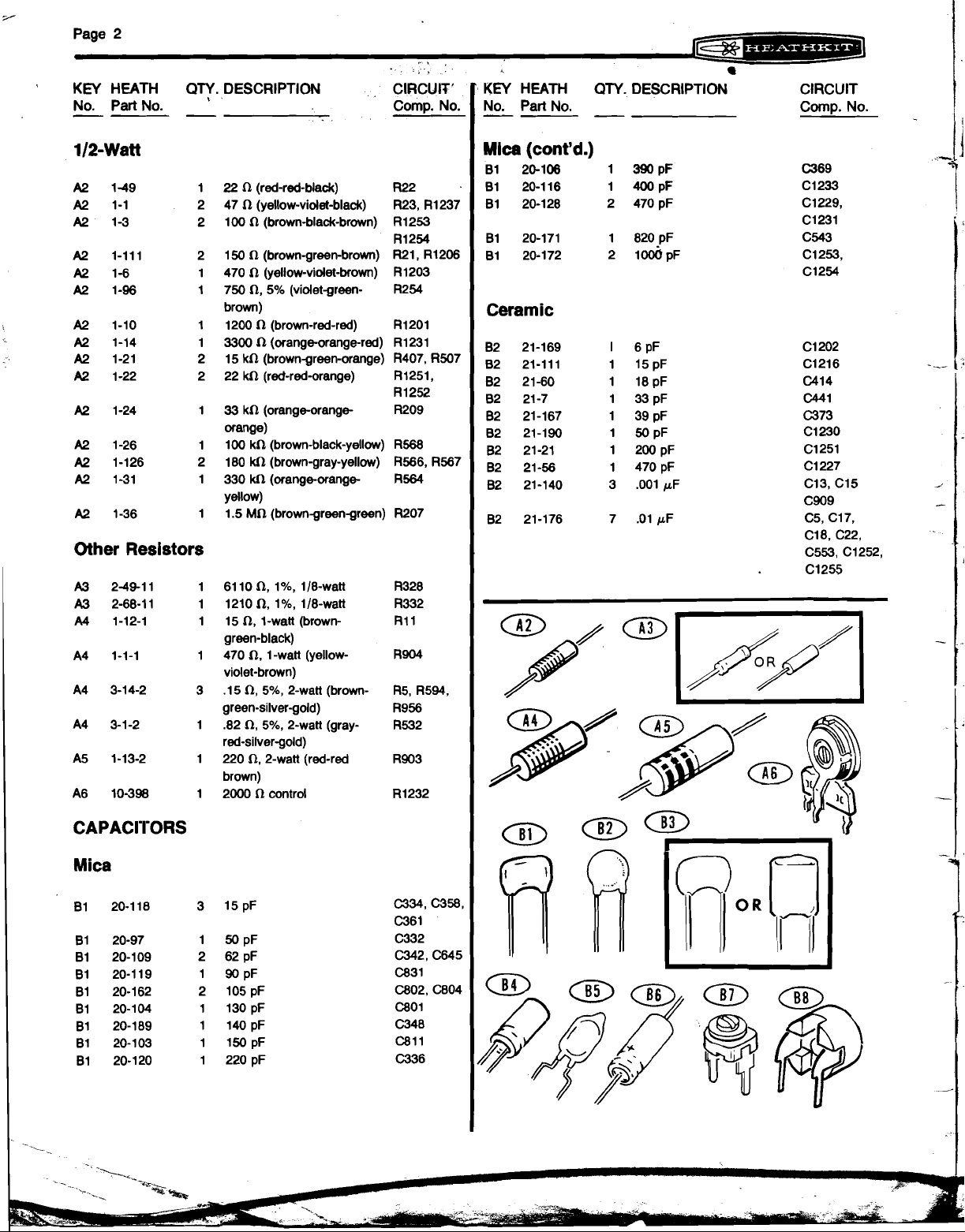
KEY
No.
-
HEATH
part
No.
QTY.
DESCRIPTION CIRCUIT
cs-
PARTS
"
3
Comp. No.
LIST
To order a replacement part, always include the
PART NUMBER. Use a Parts Order Form, or, if one is
not available, refer to "Replacement Parts" inside the
rear cover of your Transceiver Manual. For prices,
refer to the separate "Heath Parts Price List."
NOTE: The circuit component numbers refer to the
component numbers in the
.
Schematic.
-
SB-104A Manual and
2
A1
.1*!2
*,\
.
wing resistomhave a tolerance of
btherwise.
50h
\
is
10%
is
indicated by a fourth color
indicated by a fourth color band of gold.
4
100
(brown-black-brown)
a,
5
%
1 180
brown)
1
390
1
1000
1
3300
3 5600
1
6800 0,So/,
1
12 k0 (brown-red-orange)
1
22 k0 (red-red-orange)
(brown-gray-
(orange-wh~te-brown)
a
(brown-black-red)
0
(orange-orange-red)
SL
(green-blue-red)
(blue-gray-red)
BENTON HARBOR, MICHIGAN
...
10%
unless
R343,
W,
R619, R621
R13
RS14
R684
R321
R612, R677,
R679
R322
R329
R625
HEATH
COMPANY
..-
49022
/dl
Page 2
Page
2
KEY
HEATH QTY. DESCRIPTION CIRCUIT'
No. Part No.
-
I
-
22
n
(red-red-black) R22
n
(yellow-videt-black) R23, R1237
47
n
(brown-black-brown) R1253
100
n
(brown-green-brown) R21, R1206
150
470 (yellow-videt-brown) R1203
n,
5% (videtgreen- R254
750
brown)
1200 (brown-red-red) R1201
n
(orangeorange-red) R1231
3300
15 kn (browngreen-orange) R407, R507
22 kn (red-red-orange) R1251,
33 kn (orangeorange R209
orange)
kn (brown-black-yellow) R568
100
180 kn (brown-gray-yellow) R566, R567
330 kn (orangeorange R564
yellow)
MR.
(browngreengreen) R207
1.5
.. ,.
Comp. No.
R1254
R1252
KEY
HEATH QTY. DESCRIPTION
No. Part No.
-
Mlca
(cont'd.)
81 20-106 1
B1 20-116 1
B1 20-128 2 470
-
390
so0
Ceramic
~w=---~.--a~
CIRCUIT
Cornp. No.
pF
PF
pF
I
I
Other Resistors
CAPACI'I'ORS
Mica
6110 n,I%, 118-watt
n,
1210
15
green-black)
470
violet-brown)
.15 n,
green-silver-gold)
.82
red-silver-gold)
220
brown)
2000
1% 118-watt
n,
I-watt (brown-
n.
1-watt (yellow-
5%,
2-watt (brown-
n,
5%
2-watt (gray-
a,
2-watt (red-red
fl
control
Page 3
Page
3
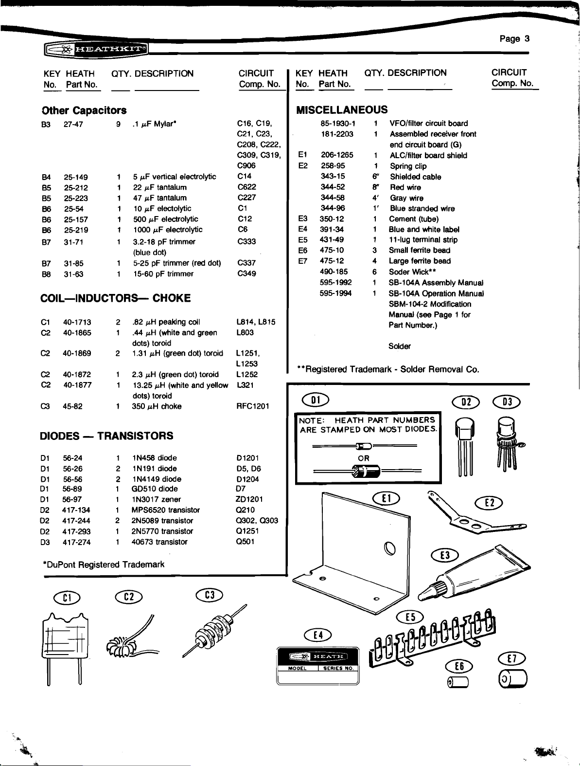
KEY HEATH QTY. DESCRIPTION KEY HEATH QTY. DESCRIPTION CIRCUIT
No. Part No. Comp. No. INo. Part No.
Other Capacitors
83
27-47 9
.I
pF
Mylar*
pF
vertical electrolytic
5
pF
tantalum
22
47
pF
tantalum
10
pF
electolytic
pF
electrolytic
500
1000
pF
electrolytic
3.2-18
pF
trimmer
(blue dot)
pF
5-25
15-60
trimmer (red dot)
pF
trimmer
COIL-INDUCTORS CHOKE
pH
C1 40-1713 2 .82
C2 40-1865 1
C2 40-1869 2 1.31
C2
40-1872 1 2.3
C2 40-1877 1 13.25
C3
45-82 1 350
peaking coil
.44
pH
(white and green
dots) toroid
pH
(green dot) toroid
pH
(green dot) toroid
pH
dots) toroid
pH
choke
(.white and yellow
cRculT
-
MISCELLANEOUS
85-1 930-1 1 VFOlfilter circuit board
181 -2203 1 Assembled receiver front
El 206-1265 1 ALClfiRer board shield
E2 258-95 1 Spring clip
343-15
344-52
344-58
344-96 1' Blue stranded wire
E3 350-12 1 Cement (tube)
E4 391-34 1 Blue and white
E5 431-49 1 1 1-lug terminal strip
E6 475-10 3 Small ferrite bead
E7 475-12
490- 185 6 Soder W~ck"
595-1992 1 SB-104A Assembly Manual
595-1994 1 SB-104A Operation Manual
**Registered Trademark -Solder Removal Co.
end circuit board (G)
6"
Shielded cable
8"
Red wire
4' Gray wire
label
4 Large ferrite bead
SBM-104-2 Modification
Manual (see Page 1 for
Part Number.)
Solder
Comp. No.
DIODES -TRANSISTORS
IN458 diode
IN191 diode
1 N4149 diode
GD510 diode
1 N3017 Zener
MPS6520 transistor
2N5089 transistor
2N5770 transistor
40673 transistor
*DuPont Registered Trademark
ARE STAMPED
ON
MOST DIODES.
Page 4
Page
4
p S L = . - - * = . - 5 + 9 J
MODIFICATION PROCEDURE
This modification kit contains all of the current mod-
ifications for your SB-104 transceiver.
To make a modification, check each component in the
following step-by-step assembly with the component
installed in your kit. If the component in your kit is
different from the one in this Manual, remove it from
your kit and install the new one at the location shown.
If
the component shown in the Manual is the same as
the one installed in your kit, disregard it and proceed
to the next step. Be careful when you remove a com-
ponent from a circuit board, or damage to the circuit
foil will occur.
When you make a chassis connection, the indicated
number of wires at the connection are shown in the
solder instructions. For example, when you connect a
wire to a solder lug where two wires are already
connected, the solder instructions will read
may be necessary to remove any excess solder from a
connection to make room for the new wire or component lead. Make sure you apply enough heat to the
connection so that solder flows to each wire or component lead.
Do not make any connections, or install any components or circuit boards, until you are instructed to do
so in a step.
When assembly or disassembly is required in a step,
refer to your
proper procedure.
SB-104A Assembly Manual for the
(S-3). It
Page 5
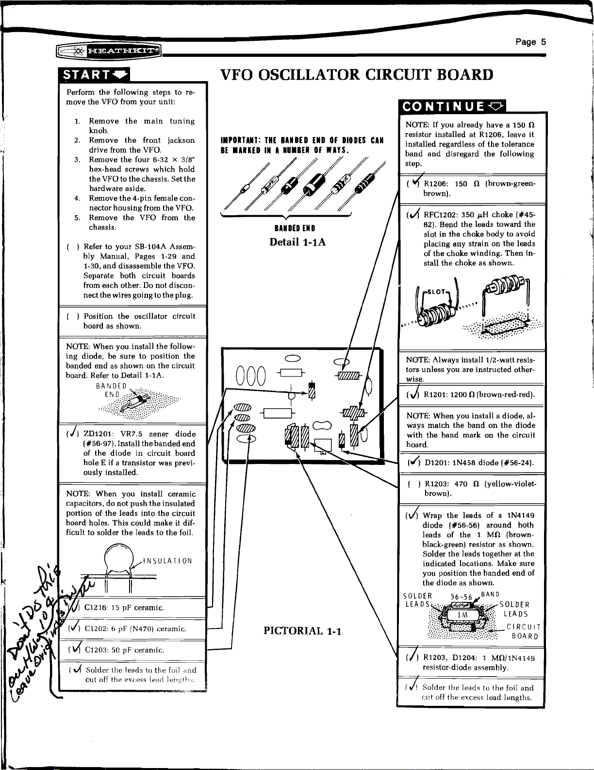
Perform the following steps to remove the VFO from your unit:
1. Remove the main tuning
2.
Remove the front jackson
drive from the VFO.
3.
Remove the four
hardware aside.
6-32 x 318"
VFO OSCILLATOR CIRCUIT BOARD
esistor installed at R1206, leave it
BANDED END
Detail
1-1A
i
1
1
of the diode in circuit board
E
if a transistor was previ-
hole
INSULATION
PICTORIAL
around both
1-1
Page 6
Page
6
(
( )
Position the VFO BUFFER cir-
I
cuit board as shown.
(/)
R1231: 3300 (orange-orange-
red).
NOTE: When you install ceramic
capacitors, do not push the insulated
portion of the leads into the circuit
board holes. This could make it dif-
ficult to solder the leads to the foil.
VFO BUFFER CIRCUIT BOARD
I
I
@%
b=*==-*=*-aii
:
47 0 (yellow-violet-
)
C1233: 400 pF mica.
)
Solder the leads to the foil and
cut off the excess lead lengths.
PICTORIAL
1-2
Page 7
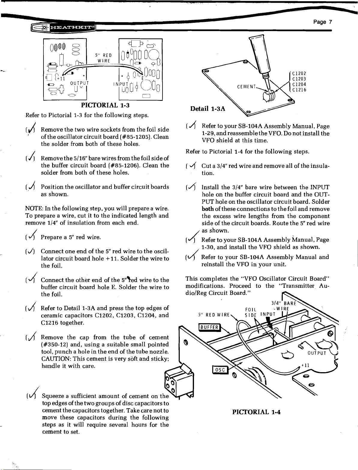
(
/r
()/J
Remove the two wire sockets from the foil side
of the oscillator circuit board (#85-1205). Clean
the solder from both of these holes.
(4
Remove the 5/16'' bare wires from the foil side of
the buffer circuit board (#85-1206). Clean the
solder from both of these holes.
(/r
Position the oscillator and buffer circuit boards
as shown.
NOTE: In the following step, you will prepare a wire.
To prepare a wire, cut it to the indicated length and
remove
(
4
-
(J)
114" of insulation from each end.
Prepare a 5" red wire.
Connect one end of the 5" red wire to the oscil-
lator circuit board hole +11. Solder the wire to
the foil.
Refer to your SB-lO4A Assembly Manual, Page
1-29, and reassemble the VFO. Do not install the
VFO shield at this time.
Refer to Pictorial 1-4 for the following steps.
(
i/j
Cut a 314" red wire and remove all of the insulation.
(4
Install the 314" bare wire between the INPUT
hole on the buffer circuit board and the OUTPUT hole on the oscillator circuit board. Solder
both
of these connections to the foil and remove
the excess wire lengths from the component
side of the circuit boards. Route the 5" red wire
J
as
(
)
Refer to your SB-104A Assembly Manual, Page
1-30, and install the VFO shield as shown.
Refer to your SB-104A Assembly Manual and
(4'
reinstall the VFO in your unit.
Connect the other end
buffer circuit board hole
the foil. dio/Reg Circuit Board."
Refer to Detail 1-3A and press the top edges of
ceramic capacitors C1202, C1203, C1204, and
C1216 together.
Remove the cap from the tube of cement
(#350-12) and, using a suitable small pointed
tool, punch a hole in the end of the tube nozzle.
CAUTION: This cement is very soft and sticky;
handle it with care.
Squeeze a sufficient amount of cement on t
top edges of the two groups of disc capacitors to
cement the capacitors together. Take care not to
move these capacitors during the following
steps as it will require several hours for the
cement to set.
of
the 5"yed wire to the
E.
Solder the wire to modifications. Proceed to the "Transmitter Au-
This completes the "VFO Oscillator Circuit Board"
5"
RED WIRE
@
-
PICTORIAL
1-4
Page 8
Page
8
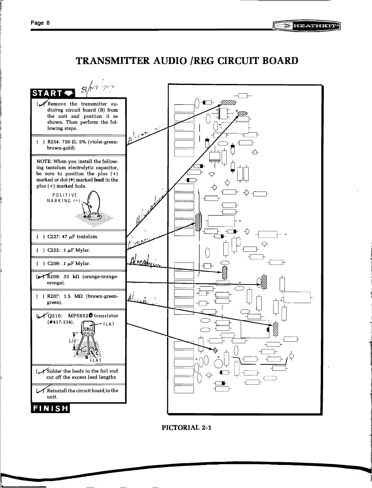
TRANSMITTER AUDIO /REG CIRCUIT BOARD
ing tantalum electrolytic capacitor,
be sure to position the plus
marked or dot
(+)
plus
(0)
marked
marked hole.
lead
(+)
in the
ircuit board-in the
PICTORIAL
2-1
Page 9
LG
b=*==-=*=*'%j
)
Remove the transmitter
(
cuit board (C) from the unit and
position it as shown. Then per-
form the following steps.
[
d~ormthe leads of a 390
watt (orange-white-brown) re-
sistor as shown. Then cut each
lead of a 39 pF capacitor to 112"
and wrap the capacitor leads
around the resistor leads. Solder
the leads together as shown.
/CUT\
(4
R314: C373: 390 a139 pF
resistor-capacitor assembly.
/
[A
4303: 2N5089 transistor
IF
n.
cir-
114-
TRANSMITTER IF CIRCUIT BOARD
Page
9
/
(
/j
R329: 12 kn. 114-watt (brown-
red-orange).
(/J
C322: Remove and discard.
C369: 390 pF mica.
R321: 3300 (orange-orangered).
(
R322: 6800 n, 5%. 114-watt
(blue-gray-red).
(
i'
4302: 2N5089 transistor
(#417-244).
BFLAT
/
I
1
(/)
C361: 15 pF mica.
/
t
(
Jcye: 15 p~ mica.
FLAT
older the leads to the foil and
cut off the excess lead lengths.
Page 10
Page 11
TOP EDGE
0
F
SPRING
Page
11
Refer to Pictorial
3-3
for the following step.
lder the spring clip to the shield in the area
wn.
(This clip will ground the shield di-
rectly to the compartment shield when the cir-
cuit board is installed.)
PICTORIAL
3-3
Page 12
Page
12
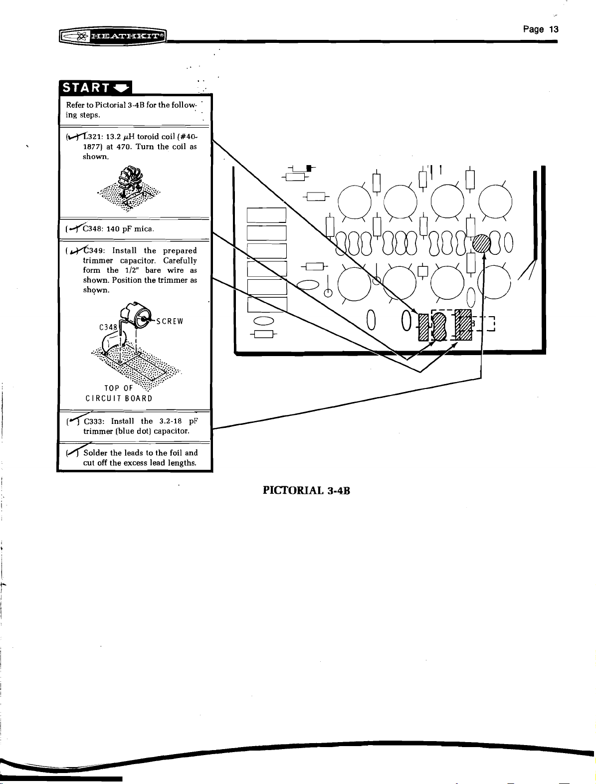
giiJ-dj
Refer to Pictorial
ing steps.
the 470 pF mica capacitor, and
the 6 pF ceramic capacitor.
the 15-60 pF trimmer capacitor.
(dut a 112" length of brown wire
and removeall of the insulation.
(Mblder
wireat the indicated location on
the 15-60 pF trimmer capacitor.
SOLDER
34A
for the follow-
CUT
OFF
one end of the 112" bare
BARE
W lRE
I
I
PICTORIAL
3-4A
Page 13
dl1nja.re3 .xo)pede3 ~aurur!q
.z/r
aql urxoj
se aqm axeq
11n:,tr1:,
atrvoa
Page 14

Page
14
HFOlPREMIXER CIRCUIT BOARD
PICTORIAL
4-1
Page 15

Page
15
1
CARRIER GENERATORIXTAL FILTER CIRCUIT BOARD
PICTORIAL
5-1
Page 16

Page
16
NOTE:
If you have the optional
filter installed, perform the following steps.
(4~679:5600 R (green-blue-red).
(4~677:5600 R (green-blue-red).
[&'R684: 1000 R (brown-black-
red).
&w*Q
CW
(Lufnstall the circuit board in your
unit.
PICTORIAL
I
5-2
Page 17

r-1
RECEIVER IFIAUDIO CIRCUIT BOARD
I
SHORTING
SPRING
Page
17
circuit board
and ~osition
board. Insert the transistor leads
(see Detail
holes on the circuit board. Solder each lead to the foil and cut
(F)
from the unit
it
as shown.
6-1A)
into the correct
Page 18

Page
18
'm
I I
POWER AMPLIFIER CIRCUIT BOARD
(
/position the circuit board as shown.
318"
NOTE:
your unit, you will have either wires and ferrite beads
or
Depending on which PA circuit board is in
.51
R
resistors installed at holes A and B.
14"
Detail
. .
7-1
Refer to Pictorial
(i)
Remove the power amplifier circuit board from
your unit and remove the heat sink. Set the heat
sink aside. Be careful not to get any of the
ma1 compound on your clothing, since it is difficult to remove.
for the following steps.
7-1A
ther-
(4'
Remove each wire and ferrite bead, or both
R
(green-brown-gold-gold) resistors, from the
circuit board at holes A and B. Discard the wires
and ferrite beads, or resistors.
(d
Refer to Detail
2-watt (brown-green-silver-gold) resistors as
shown.
(/(
Install one prepared resistor on the circuit
board at hole A and the other prepared resistor
at hole
locations and cut off the excess lead lengths
from the foil side of the circuit board.
B.
7-1A
and prepare two
Solder each resistor at the indicated
.15
R.
.51
5%
PICTORIAL 7-1
Page 19

&#J===--,-==-@di
Page
19
Refer to Pictorial
)
Turn the power amplifier circuit board over
8-1
for the following steps.
(foil side up) and unsolder the wire at hole
(
)
Decrease the turns of wire, through the two
brass tubes, by one turn (five to four).
(
)
Route the wire back to hole Mand cut off the
excess wire length at that point. Discard the
excess wire,
0
0
-6
5/4
1
(INCHES)
I.I,l.I1l,I.I.I,I,I.l,l.l
1 (CM) 2 3 4 0 6 7
' I ~ I ~ I ~ I ~ I ~ I ~
2
PICTORIAL
(J]
AA.
(J)
I/
(
(
d
3
B
0
8-1
Prepare the free end of the wire and apply a
small amount of solder to the wire strands to
hold them together. Solder the wire to hole
Unsolder the wire at hole
AB
and repeat the
three previous steps.
/
)
Reinstall the heat sink on the circuit board.
)
Install the circuit board in your unit.
4
.l,l.l.l.l,I,I.I.I.I,
10 11 12 13 14 10 16 17
5
6
AA.
7
Page 20

Page 21

c-35
ALCIOUTPUT CIRCUIT BOARD
board
(K)
position it as shown.
Cut the wire from the top wafer
(
switch SWlC between lugs 12
an? 14.
/
ut a
and remove the insulation.
from your unit and
318"
length of gray wire
I
DETAIL 10-1A
Page
21
I
d~eferto Detail 10-IA and solder
318"
bare wire between wafer
the
PICTORIAL
10-1
Page 22

SZB?
,r
(
)
JO
aj!q d~eqs e asn
OMJ
aql le ~!oj aqlln3 pue
apelq rozeJ pa8pa-a18u!s
.suo!le~o~paleznpu!
:st81
aql Japlos
pea1 1!03 paa~n~
01
1!o3 pa~eda~d
1!0j aqlol
aql JaploS au~oqs se pnoq 1!n3~!3 aql jo ap!s
aql daa>~ .~!oj puno~8 aql
$1 leql os poj aql jo a8pa ap!su! aqlol asop peal
-u! 8u!mp s!sseq~ aql ql!~ aJapalu! lou saop
lsu!e%e 1q8!l dpoq 1!03 aql uo!~!sod .uo!leIlels
.pJeoq 1!n3~!3 aql
06
)
(
:r~83
sso~~e
\!OD
aql JaploS
vr87
pa~eda~d
aql uo!l!sod
~olpede:, e3!u1 ~d
gn3q3 aql jo ap!s 1!0j aq u~og
dpoq ~opede~ .u~oqsse p~eoq
.pJeoq l!n3~!3 aql lsu!e8e lq8!l
Page 23

L@@J=**--=*+El
VFOIFILTER CIRCUIT BOARD
Page
23
Position the VFOIfilter circuit boardp
(#85-1930-1) as shown and complete
the following steps.
NOTE: To prepare a length of wire,
cut it to the indicated length and remove 114'' of insulation from each
end.
(\n/prepare a 1-314'' gray wire. Re-
move an extra 114" of insulation
from either end of the wire.
Then insert the
end in hole
wire to the foil. The free end of
this wire will be connected later.
/
(4
L1253: Toroid coil (#40-1869).
C1254: 1000 pF mica.
114" stripped
D
and solder the
.
.
1
6~1255:
(drepare a 1-314" red wire. Then
1
(61253: 100
(
,&€1252:
(
d51: 22 k0 (red-red-orange).
(
Molder the leads to the foil and
(
4~1251: 2N5770 transistor
.O1
@F ceramic.
insert one end of this wire in
hole C and solder the wire to the
foil.will be The free end later. connected of this wire
0.
(brown-black-
brown).
.O1
@F ceramic.
cut off the excess lead lengths.
(#417-293). First lineup the flat
on the transistor with the outline of the flat on the circuit
board. Then insert the transistor
leads into their corresponding
holes indicated by E, B, and C.
Solder the leads to the foil and
cut off the excess lead lengths.
I
I
I
(4
L1252: Toroid coil (#40-1872).
(J)
C1253: 1000 pF mica.
)
L1251: Toroid coil (#40-1869).
(
(4
R1254: 100 R (brown-black-
brown).
(
1~1252:22
(9
C1251: 200 pF ceramic.
(
/)"solder the leads to the foil and
cut off the excess lead lengths.
(
]
Squeeze a little cement into the
centers of the three toroid coils
to affix them to the circuit
board.
kR
(red-red-orange).
Prepare a 6" shielded cable. Re-
(
move 314" of outer insulation
and 114" of inner insulation
from both ends of the cable.
(
XConnect the inner lead of the 6"
shielded cable to hole
shield lead to hole B. Solder
both leads to the foil and cut off
the excess lead lengths. The free
end will be connected later.
Proceed to "Installation of the New
VFOIFilter Circuit Board."
A
and the
I
Page 24

1
*ax
PI
01
IBU
T-ZT
1syol3!d
'3
saIOq le pmoq
su!d'pa
'~3
aql aoj
'A
'3
'a
'8a
'~a
'3
-u~oqsse s!sseq~ aql uo!l!sod
pue
pue '6a
.sdals
%U!MOIIOJ
'H
'OTC~
Y
x
aql aAomax
le pnoq
qn=a!= aalI!j/odA am uo saa? 6818 x!s aq In3
-!ma) )e saa? ~ea~am pmos!p pue anomax x!s
/
Y
€3
suld leu
g#
OM$
aql pue s~ams
'nv
pue
>nr
.A1!naodmal
-m
pm
PIO
Iepw laaqs peaq-xaq ,8/s
l!n3q3 aq moq saa~eds ,,8/~
ap!se aaeMpnq aql $as
-!maal moq saqM alqe3 paplays aql aap~osun
'pnoq l!n3~!3 J~~I!J/O~IA aql Pn3s!
Page 25

Page 26

Page
26
@%+-ii
i
CABLE
#3
PICTORIAL
13-1
Page 27

gg-T-2
CIRCUIT BOARD
I
I
#6
x518"
HEX HEAD
HEET METAL
SCREW
I
Page
27
Refer to Pictorial 13-1 for the following steps.
(
u)/~efer to Detail 13-1A and install the new circuit
board on the chassis. Use the two hex-head
sheet metal screws and the two 118" spacers that
you previously removed at AK and AM.
(A
Connect the free end of the 1-314'' red wire
ing from circuit board hole C to terminal pin Dl
(S-3).
Install a small ferrite bead on the free end of the
4''
[
1-314" gray wire coming from circuit board hole
D. Connect the wire with the ferrite bead to
terminal pin D4 [S-11.
Detail
corn-
13-1A
(
df
Disconnect the shield wire on shielded cable
#3 at terminal pin G3 and install a small ferrite
bead on the shield. Reconnect the shield to terminal pin G3 (NS). NOTE: It may be necessary
to remove an extra 114" of outer insulation from
the shielded cable to make the shield longer.
(Aonnect the inner lead of the shielded cable
coming from the VFOIfilter circuit board to
terminal pin G4 (S-3). Then install a ferrite bead
on the shield lead and connect the lead to terminal pin G3 (S-4). Dress shielded cable #3 as
shown.
This completes the "Installation of the New
ter Circuit Board." Proceed to "Chassis Changes."
VFOIFil-
Page 28

Page 29

Page
29
CHASSIS
discard the .33 R resistor con-
(
dconnect the positive
trolytic capacitor to transistor
Connect the other lead to phone jack
C14: Connect the positive
(4
vertical electrolytic capacitor to terminal strip
BE
lug 3 (S-4). Connect the other lead to lug
(
+Tf
your unit has a .1pF ceramic capacitor instal-
led between terminal pins C2 and C4, remove it.
-6:
Connect a .1 pF Mylar capacitor between
terminal pins C2 (S-3) and C4 (S-2).
(+)
lead of a 1000 pF elec-
42
(+)
lead of a 5 pF
lug B (S-2).
J2
lug
1
4
CHANGES
(
kC1: Connect the positive
electrolytic capacitor to terminal pin C7 (S-2).
Connect the other lead to solder lug AH (S-5).
(
4R22: Connect a
tween terminal pin D4 (S-2) and solder lug AL
(S-3).
(
d"
C19: Connect a
terminal pin Dl5 (S-3) and solder lug AN (S-2).
(
d"
C18: Connect a
tween terminal pin F8 (S-21 and the indicated
solder lug at AP (S-2).
(dC13: Connect a .001 pF ceramic capacitor be-
tween terminal pins F13 (S-3) and F15 (S-3).
J
(
)
R23: Connect a
tor between terminal pin G4 (S-3) and solder lug
AT (S-5).
C21: Connect a
terminal pins GI9 (S-2) and G21 (S-2).
Remove and discard the .lpF ceramic capacitor
(
/
between terminal pin K5 and solder lug
(/)
C15: Connect a .001 pF ceramic capacitor at
relay RY between lugs 10 (S-2) and ITS-3).
22
R
.1
pF Mylar capacitor between
.O1
47
R
.I
pF Mylar capacitor between
(+)
lead of a 10 pF
(red-red-black) resistor be-
WF ceramic capacitor be-
(yellow-violet-black) resis-
BJ.
(
&&4:
Connect a
terminal pin C6 (S-2) and solder lug AH (S-4).
Do not allow the lead of this capacitor, that is
connected to terminal pin C6, to touch the leads
of the .01 pF ceramic capacitor.
.1
pF Mylar capacitor between
(
/
)
C12: Connect the positive
electrolytic capacitor to terminal pin
Connect the other lead to phono socket CA lug
(S-3).
(+)
lead of a 500 pF
J1
(S-5).
2
Page 30

Page
30
ce
b=**-*=*=*]
Refer to Pictorial 14-2 for the following steps.
(
y)i
Unsolder the 3-314" gray wire at terminal pinK5
and slide the four large ferrite beads over the
wire as shown.
NOTE:
ferrite bead. Then, when you install the gray wire,
push the beads down against the chassis so the cement will hold them to the chassis.
(v)/
In the next step, apply a drop of cement to each
the
3-314" gray wire with the ferrite
byads to terminal pin K5 (S-1).
Connect a
RY between lugs 13 (S-3) and 14 (S-2).
Unsolder the end of the 5" orange wire at relay
RY lug
nal Jl), and reconnect the wire to terminal
(S-3).
.O1
pF ceramic capacitor at relay
11
(the other end is connected to termi-
H6
/
Unsolder the end of the 4" orange wire at termi-
(
)
nal
Jl
(the other end is connected to terminal
K3), and reconnect the wire to relay RY lug
(S-2).
Cut the ends of the two heavy orange wires,
(J)
coming from
(4)
Prepare the ends of two heavy orange wires and
reconnect them to terminal F19 (S-2). Shorten
the wires as necessary.
Refer to Pictorial 15-1 for the following steps.
(J)
Prepare a 10" gray wire.
Connect one end of the 10" gray wire to terminal
(J)
pin F7 (S-21, and route the other end through
grommet
BA.
BO
#5, at terminal
J1.
11
Page 31

c--=*~*g
i
Remove and discard the red wire connected
between terminal pins G2 and G13.
PICTORIAL 15-1
CONTROL
Page
31
Route the heavy orange wire coming from ter-
minal pin B2 to terminal pin G2. Cut the heavy
orange wire at the G2 junction and prepare the
two wire ends. Make sure you allow eqough
slack at both ends of the wire before you cut it.
Connect both orange wires to terminal pin G2
(S-2).
Refer to Detail
shown. Then connect the free end of the 10"
gray wire coming from grommet BA to rear
panel access socket CY pin 3 (S-1). Be careful
not to burn any insulation on the adjacent
wires.
15-1A and position the chassis as
Refer to Pictorial 16-1 for the following steps.
he two gray wires at control R2 lug
ove and discard the short gray wire con-
d to the control ground lug.
e the free end of the remaining gray wire
d connect it to the control
6.
Detail
repare a 5" gray wire.
PANEL
one end of the 5" gray wire to terminal
lug 3 (S-3). Connect the other end to
15-1A
Page 32

Page
p
32
c a J = ' * " *
CUT
=*:-4l]
I
SHIELD
WAFER
LI
ARD
Detail 16-3A
CW CRYSTAL WIDE AND NARROW MODIFICATIONS
Refer to Pictorial 16-3 for the following steps.
NOTE: When you complete the following modifica-
tions, the SSB filter will be enabled when
switch is out, and the CW filter will be enabled when
the90
(/f
Hz
switch is in.
Remove and discard the gray jumper wire between terminal pins E9 and E17.
the*^
Hz
PICTORIAL 16-2
Refer to Pictorial 16-2 for the following steps.
(A'
Position the chassis as shown.
/
(
i/
R11: Remove the 15 a,112-watt (brown-greenblack) resistor from S1 wafer A lugs
a,
Install a 15
1-watt resistor in its place.
1
and 3.
[
$'
Remove the white-orange wire at terminal pin
E9 and connect it to terminal pin El7 (S-2).
(A
Refer to Detail 16-3A and prepare the 11-lug
terminal strip as shown. Use diagonal cutters to
cut through the terminal strip insulator. Save
the indicated sections.
(
4
Remove the hex-head screw at chassis hole AM
and install the prepared 3-lug terminal strip as
shown.
1
(4
Install a IN4149 diode (#56-56) at terminal
strip AM between lugs
nect the banded end at lug 3.
(
4
Cut a 1-518" gray wire and remove all the insulation.
(J;/
Connect the 1-518" gray wire between terminal
strip AM lug 3 (S-2) and terminal pin El0 (S-2).
,--.
(
)
Remove the white-black wire from switch E lug
[
,
j
4 and connect it to switch ilug 6 (5-11.
2
(NS) and 3 (NS). Con-
Page 33

C-&---=*=@l
(
4
Remove the gray wire from switch E lug
move 314" of insulation from the wire end. You
will connect it later.
(
r)/~emove the jumper wire between switch E lug
and switch F lug
fl
Remove the two red wires from switch E lug
and reconnect them to switch F lug 2 (S-2).
(
4
Prepare two 1" gray wires.
(
/Connect one 1" wire to switch E between lugs
(S-1) and 6 (NS).
(~"~onnectthe remaining 1" wire to switch E be-
tween lugs
(
vf
Prepare a 7-112" gray wire.
(&,Connect one end of the 7-112" gray wire to
switch
minal strip AM lug
E
lug 6 (S-2) and the other end to ter-
5.
2
(S-1) and 5 (NS).
2
(S-2).
6.
Re-
1
Page
33
6
1
NOTE: When a wire passes through a connection and
then goes to another point, as in the next step, it will
count as two wires in the solder instructions (S-2),
one entering and one leaving the connection.
(
Lh/
Connect the gray wire, with the 314" prepared
end, to switch
4-w).
lug
(vj"Prepare the following gray wires:
(d
Connect one end of the 5"gray wire to switch
lug 3 (S-1) and the other end to terminal pin B14
(S-4).
(/connect one end of the 9-114" gray wire to
switch
nal pin E9 (S-2).
This completes the "CW Crystal Wide and Narrow
Modification." Proceed to "RFDetector Installation."
E
F
through lug 5(S-2) to switch E
cs-1)
E
lug 5(S-2) and the other end to termi-
PICI'ORIAL
16-3
;.
::
5
Page 34

Page
34
cm=*-+-*=*:*g
RF DETECTOR INSTALLATION
Re r to Pictorial 16-4 for the following steps.
Position the chassis as shown.
)
l
(d
Remove the 180 I1(brown-gray-brown)resistor
across the meter terminals.
Refer to Pictorial 16-5 for the following steps.
Position the chassis as shown.
4f'
(
(
d
Prepare a 2" gray wire. Remove an extra 114" of
insulation &omone end of the wire (112") total.
(
d
Connectthe 112"stripped end of the 2" gray wire
to switch B through lug 5(S-2)to switch A lug 6
(S-1). Connect the other end to switch C lug
(NS)
1
(d
Connect a 180
between switch Clug 5 (S-2)and switch
(NS)
(d
Prepare a 2-112" gray wire.
I1
(brown-gray-brown)resistor
,
PICTORIAL
5
D
lug 5
16-4
GRAY GRAY
S
0
Q
-
8
-
(L+
Connect one end of the 2-112" gray wire to
D
switch
E
lug 4 (S-2).
lug 5 (S-2)and the other end to switch
PICTORIAL
16-5
Page 35

Page
35
PICTORIAL 16-6
Refer to Pictorial 16-6 for the following steps.
(vfiosition the chassis as shown.
(
l.-+"?~isconnect the white-red wire at control Rls
lug
5
and prepare the end.
(
$/Refer to Detail 16-6A and connect the white-red
wire to switch
C
lug 2 (S-I).
S
69
/
WHT -RED
WIRE
Detail
16-6A
Page 36

Page
36
'fl~zGl
Refer to Pictorial
(
]
Remove the jumper wire at switch
2
lugs
(
)
Unsolder the red wire at switch D lug 5 and
reconnect it to lug
and
16-7
for the following steps.
5.
2
(S-2).
GRAY
PICTORIAL
D,
\\
[
16-7
)
Prepare a
Connect one end of the 2"gray wire to switch
)
lug
(S-3).
5
(S-1)
2"
gray wire.
and the other end to switch E lug
D
2
a
a
1/4
0
.6 1 (cu)
~ a
3/4
, 1 , (INCHES), ,
l ' l ' l ' l ' l ' l ' l ~ l ' ~ ~ ~ ~ ~ ' ~
a
3
2
1
, ~
4
6
6
3
1
7 a
,
,
B
4
I
I . l . I , I . l ~ I , I . 1 , r . I ~ ; I
10
9 9
5
12
13
14 16 16 17
6
7
Page 37

PICTORIAL 17-1
Page
37
Refer to Pictorial 17-1 for the following steps.
(
\/:
Remove both 1kfl (brown-black-red) resistor
leads at terminal pins GI3 and G15.
,
(
d'
Remove the 2" gray wire at terminal pin G24.
(
d'
Remove both leads of the shielded cable from
terminal strip AE lugs 2 and 3.
PICTORIAL 17-2
(JRemove and discard the 8.65 MHz trap (termi-
nal strip AE) from the chassis. Save the screw
but do not reinstall it at this time.
Refer to Pictorial 17-2 for the following steps.
Position the prepared 4-lug terminal strip as
(L:)
shown.
pF
a .01
lugs
1
(NS) and 2 (NS).
(d
Connect a 150 fl (brown-green-brown) resistor
between lugs 2 (NS) and 3 (NS).
Connect a
(NS] and 4 (NS).
(/connect the banded end of a IN191 diode
(#56-26) to lug 2 (NS) and the other end to lug 3
(NS).
(dconnect the banded end of a lNl9l diode
(#56-26) to lug 4 (NS) and the other end to lug 2
IS-4).
.1
pF
ceramic capacitor between
Mylar capacitor between lugs 3
the banded end of a 6D510 diode
(#56-89) to lug 3 (S-4) and the other end to lug 4
(NS).
Page 38

Page
p-
38
b=*---=*-&$jJ
1
PICTORIAL
Refer to Pictorial
(
J~emove the white-red wire from terminal pin
G5. (S-2).
(
hut a
tion.
Connect the
G5 [S-1)
17-3
for the following steps.
1-114"
gray wire and remove all the insula-
1-11'''
bare wire from terminal pin
to solder lug AT
(S-6).
/
(,/f
Reconnect the shield lead from the shielded
cable to terminal pin
inner lead to terminal pin
cable and prepare' the end as necessary.
(
d'
Mount the wired 4-lug terminal strip to chassis
hole AE with the screw you removed earlier.
/
(d
Connect the white-red wire, which you removed from terminal pin
AE
lug
4 (s-4).
NOTE: pull the white-red wire
through the wire harness if it is not long
enough.
,G23 [S-2).
G24 (S-1).
G5,
to terminal strip
Connect the
Cut the
17-3
6"
Prepare a
[
d~onnectone end to terminal strip AE lug
length of blue stranded wire.
I
NOTE: You will use the free end of the blue stranded
wire as a probe during the "Alignment" section. In
the following step, ''tack'' solder the connection since
the wire will be moved later.
(
vf
Connect the free end of the
wire to terminal pin
(
K~urn
the chassis over and install the new re-
ceiver front end circuit board
G5 (S-2).
6ff
blue stranded
(G)
in your unit.
This completes the "Chassis Changes." Proceed to
Pictorial
18-1.
s/,
1
0
1/4
I ' I ' l ' l ' l l l l ~ l ~ ~ I g ~ l l ~ ~ l
0
.s
1 (CM) 2 3 4
(INCHES)
2
5
6 10
3
4
11
5
12 13 14
6
15
16 17
7
Page 39

&
~=---~=*~d
Page
39
u
&e&
&3
u
o
\
END
OF
SWITCH SHAFT
I
I
II I
I
1
I
I
I
/'
Refer toPictoria1 18-1 for the following steps.
Position the chassis as shown.
(
d~oosenthe collar setscrew on the Band switch
shaft. Pull the shaft out so the end is in front of
the converter as shown.
(
Aemove the ALC circuit board from the chassis.
(
fiemove the driver circuit board from the right
side panel.
(/Remove the right side panel from the chassis.
Remove the converter hardware at BG and BH.
(li(
Position the ALClfilter circuit board shield
under the converter as shown. Then reinstall
the converter hardware at BG and BH.
(
d'
Reinstall the ALC circuit board and Band
switch shaft. Tighten the setscrewon the collar.
(
fleinstall the right side panel and the driver
circuit board on the chassis.
PICTORIAL
18-1
"
w
I
I
\
.s,
L//Mark your new Operation Manual so you per-
form the following adjustments after the "Low
Power Transmitter Check" but before the "CW
Check."
This completes the SBM-104-2 modifications. Proceed to the SB-104A Operation Manual VFO Adjustment section and perform the balance of the "Alignment Procedure."
Page 40

Page
40
t ~ ~ ~ = m
/
Fifteen Meter Power Adjustment
Unplug circuit board C from compartment CC.
(1
)
Then plug your extender board into compartment CC.
0)
Plug circuit board C into the extender board.
(
J
)
Set the BAND switch to 21.0.
(
)
Depress the ON, ALC, and USB buttons. Be sure
the HI button is released.
(J
)
Refer to the inset drawing on Pictorial 19-1 and
preset trimmer capacitor C349 to maximum
capacity (silver portion positioned as shown).
Tune the Transceiver to 21.250.
(
/
)
( J )
Rotate the MIClCW LEVEL control fully
clockwise.
Push the TUNE button and adjust trimmer C333
[I
1
.
.
on circuit board C for maximum meter indica-
tion. Use the MIC/CW LEVEL control to keep
the meter near midscale.
PICTORIAL
(
(
Twenty Meter Power Adjustment
(
(
(
(,)
(
(I/
( v )
19-1
Check the meter indications at 21.0 and 21.450.
4
If the two indications are not the same, readjust
trimmer (2333 a small amount until the indica-
tions are the same.
Release the TUNE and On buttons.
d')
Set the BAND switch to 14.0.
)
Depress the
i)
the HI button is released.
/)
Tune to 14.12.
Rotate the MICICW LEVEL control fully
clockwise.
1)
Push the TUNE button and adjust trimmer C337
on circuit board C for a maximum meter indica-
tion. Use the MIClCW LEVEL control to keep
the meter near midscale.
Release the TUNE button.
)
Depress the PWR and TUNE buttons.
ON,
ALC, and USB buttons. Be sure
Check the meter indications at 14.0 and 14.350.
(
Release the TUNE button.
(
d
)
Depress the PWR and TUNE buttons. tions are the same.
(
J)
j)
If
the two indications are not the same, readjust
trimmer
C337
a small amount until the indica-
Page 41

Page
41
a--=q
PICTORIAL
Release the TUNE and ON buttons.
(
i
( )
Unplug the circuit board C from the extender
board. midrange.
Remove the extender board.
(
-
1
NOTE: When you install the circuit board in the next
step, push down each end of the spring clip mounted meter.
to the coil shield until the board is completely seated.
[
Plug circuit board C into its compartment. Visually check to make sure the peaking coils do
not touch the metal shield. If necessary, bend
them over enough to clear the shield.
Ten Meter IFlPredriver Filters
(
4
Make sure your dummy load is connected to the
ANT socket.
NOTE: The coil adjustments in the following steps
should not require tuning the coil slugs more than 114
turn from the factory setting. Be sure to correctly
identify each coil before inserting the alignment tool.
Be sure the meter drops to 0 when the LEVEL control
is fully counterclockwise.
(4
Depress the ALC and ON buttons.
19-2
NOTE: During the following coil adjustments, the
ALC indication will vary with the setting of the
MlCICW LEVEL control. Keep the meter reading at
(4
Depress the TUNE button.
(
4
Adjust coil L310 for a peak indication on the
(
4
Release the TUNE button.
(
4
Turn the BAND switch to 29.0 and tune the
Transceiver to 29 100.
(4'
Depress the TUNE button.
(
4'
Adjust coil L319 for a peak indication on the
meter.
(
4
Release the TUNE button.
(4
Turn the BAND switch to 29.5 and tune the
Transceiver to 29 600.
(A
Depress the TUNE button.
(4
Adjust coils L309 and L320 for a peak indication on the meter. Repeat the adjustment until
no higher reading can be obtained.
Refer to Pictorial 19-2 for the following steps.
(
4
Turn the>BAND switch to 28.0.
I
4
Tune the Transceiver to 28 100.
(4
Repeat the foregoing series of steps two or three
times until you are sure the maximum reading
has been obtained.
(4
Release the TUNE and ON buttons.
 Loading...