

HDJ WIRELESS ENTERPRISE d b a NIVIS VN3104034R5 User Manual
VersaNode 310-I Hardware Integration
Application Note
Version 3.0
Date: May 24, 2013
08-00030-01 R3 Proprietary & Confidential – Nivis, LLC.

Table of Contents
1. Purpose and Audience.......................................................................................................... 3
2. Interface Summary ...............................................................................................................3
3. Serial and SPI Interfacing with VN310-I.................................................................................. 6
4. VN310-I Power Supply Considerations................................................................................... 8
4.1 Key Specifications................................................................................................................ 8
4.2 Electrical Characteristics....................................................................................................... 8
4.3 External antenna specifications and installation requirements ..............................................10
5. VN310-I Mechanical Drawings............................................................................................11
6. Regulatory Labeling and Notices.........................................................................................15
08-00030-01 Rev. 3.0 VN310-I Hardware Integration Application Note 10/07/2011
Proprietary & Confidential – Nivis, LLC.
1. Purpose and Audience
The purpose of this document is to define the VN310-I radio’s connectivity options. It also aims to
provide the necessary data to achieve hardware integration of the VN310-I with a customer’s external
application processor.
An external processing entity can communicate with the VN310-I using either a UART interface (utilizing
UART2) or an SPI interface. The UART1 port is dedicated to serial firmware download.
By definition the VN310-I is essentially a small radio module, approximately 1.1”W x 1.4”L, which is preloaded with the Nivis ISA100.11a communications stack. The small form factor enables the radio to be
used in a variety of applications. The VN310-I and the VN310-H are identical from a hardware
perspective and differ only by the pre-loaded factory firmware.
2. Interface Summary
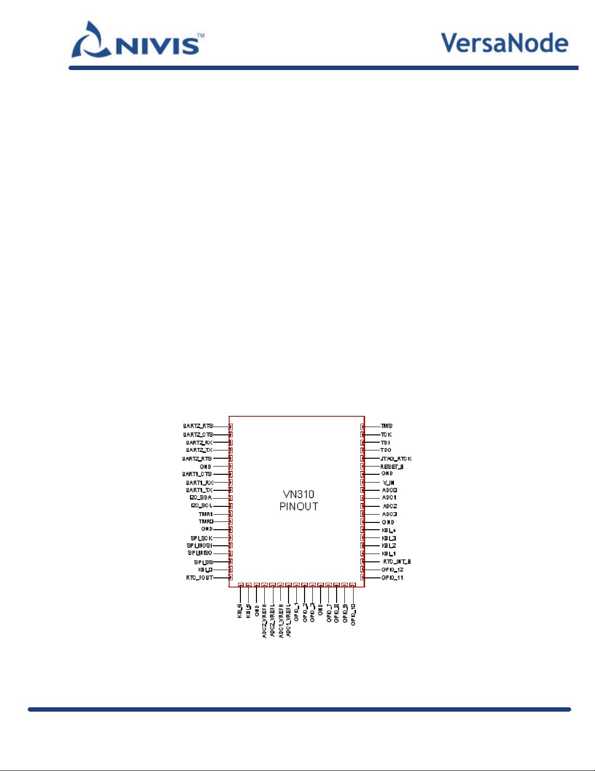
Figure 1 presents the physical location of the pins on the VN310-I, and Table 1 presents the VN310-I pin
descriptions.
Note: For minimum battery consumption, all unused GPIOs should be left unconnected.
Figure 1. VN310-I Pinout
08-00030-01 Rev. 3.0 VN310-I Hardware Integration Application Note 10/07/2011
Proprietary & Confidential – Nivis, LLC.
Table 1. VN310-I Pin Definitions
No. Name Description Type Dir Comments
1 UART2-CTS UART2 Clear to Send DIG I Standard UART communication with flow
control. Connect this to UART-RTS of application
processor.
2 UART2-RTS UART2 Request to Send DIG O Standard UART communication with flow
control. Connect this to UART-CTS of application
processor.
3 UART2-RXD UART2 Receive Data DIG I Standard UART communication with flow
control. Connect this to UART-TXD of application
processor.
4 UART2-TXD UART2 Transmit Data DIG O Standard UART communication with flow
control. Connect this UART-RXD of application
processor.
5 UART1-RTS UART1 Request to Send DIG I Not Used
6 GND Ground N/A N/A
7 UART1-CTS UART1 Clear to Send DIG O Not Used
Standard UART communication. Used for
8 UART1-RXD UART1 Receive Data DIG I
9 UART1-TXD UART1 Transmit Data DIG O
10 I2C-SDA I2C bus DATA DIG I/O Not Used
11 I2C-SCL I2C bus CLOCK DIG I/O Not Used
12 TMR1 Timer 1 I/O DIG O READY signal used to wake up the application
13 TMR0 Timer 0 I/O DIG I/O Not Used
14 GND Ground N/A N/A
15 SPI-SCK SPI Clock DIG O Standard SPI Communication
16 SPI-MOSI SPI Data Out DIG O Standard SPI Communication
17 SPI-MISO SPI Data In DIG I Standard SPI Communication
upgrading the firmware of the VN310-I. TTL<->
RS232 level shifters should be employed when
connecting to RS232 port.
Standard UART communication. Used for
upgrading the firmware of the VN220. TTL<->
RS232 level shifters should be employed when
connecting to RS232 port.
processor.
18 SPI-SS SPI Slave Select DIG O Standard SPI Communication
19 KBI0 RTC clock out enable /
Keyboard interface pin 0
DIG O Not Used
08-00030-01 Rev. 3.0 VN310-I Hardware Integration Application Note 10/07/2011
Proprietary & Confidential – Nivis, LLC.
No. Name Description Type Dir Comments
20 RTC-FOUT 32768Hz RTC clock out DIG O Not Used
21 KBI6 Keyboard interface pin 6 DIG I Used for Wakeup & Status (Provisioning) button.
Holding this pin low for 10 seconds causes the
radio to return to the factory defaults state and
scan for a provisioning device.
22 KBI5 Keyboard interface pin 5 DIG I/O Not Used
23 GND Ground N/A N/A
Set ADC2-VREFH to Low and ADC2-VREFL to
High and power the VN220 for a few seconds to
erase the flash. After erasing the flash, set the
ADC2-VREFH to High and ADC2-VREFL to Low.
WARNING: this operation will erase the Nivis
Bootloader and all manufacturing and
non-volatile data!
24
ADC2VREFH
ADC2 reference, high pin Analog I
25
26
27
28 GPIO1 GPIO DIG O Used for output gain control.
29 GPIO2 GPIO DIG O Used for output gain control.
30 GPIO3 GPIO DIG O Used for output gain control.
31 GND Ground N/A N/A
32 GPIO7 GPIO DIG I/O Not Used
33 GPIO8 GPIO DIG I/O Not Used
34 GPIO9 GPIO DIG I/O Not Used
35 GPIO10 GPIO DIG I/O Not Used
36 GPIO11 GPIO DIG I/O Not Used
37 GPIO12 GPIO DIG I/O Not Used
38 RTC-INT-B RTC wake -up interrupt /
ADC2VREFL
ADC1VREFH
ADC1VREFL
ADC2 reference, low pin Analog I See the comments for ADC2-VREFH.
ADC1 reference, high pin Analog I Not Used
ADC1 reference, low pin Analog I Not Used
DIG O Not Used
Keyboard interface pin 7
39 KBI1 Keyboard interface pin 1 DIG I Used as boot switch in order to boot different
firmware images based on the position of the
switch (future functionality). At present, this pin
should be held HIGH.
08-00030-01 Rev. 3.0 VN310-I Hardware Integration Application Note 10/07/2011
Proprietary & Confidential – Nivis, LLC.
 Loading...