

HDJ WIRELESS ENTERPRISE d b a NIVIS NIVISVN400 User Manual

Certification Exhibit
FCC ID: SQB-NIVISVN400
IC: 6546A-NIVISVN400
FCC Rule Part: 15.247
IC Radio Standards Specification: RSS-210
ACS Project Number: 12-0358
Manufacturer: Nivis, LLC
Model: VersaNode 400
Manual
5015 B.U. Bowman Drive Buford, GA 30518 USA Voice: 770-831-8048 Fax: 770-831-8598

08-00040-02.2
VN
400
Hardware
Integration Application Note
Page1/1Proprietary &
Confidential
–
NIVIS LLC
VersaNode 400 Hardware Integration
Application Note
Version 2.2
Date: January 4, 2013
VN
400
Hardware
Integration Application Note
Page2/2Proprietary &
Confidential
–
NIVIS LLC
Revision History
Date Version Description Name
11/8/12 1.0 Initial Release K. Scott
11/30/12 2.0 Added FCC/IC Info
Corrected footer and formatting
12/6/12 2.1 Added Figure 3 to show J2 Pin 1 location K. Scott
1/3/13 2.2 Added FCC two part warning
Updated Dimension Drawing
K. Scott
K. Scott
Table of Contents
1. Purpose and Audience ............................................................................................................................................ 3
2. Pin-out and Interface Summary .............................................................................................................................. 3
3. VN400 Power Supply Considerations ...................................................................................................................... 8
3.1 Key Specifications................................................................................................................................................... 8
3.2 Electrical Characteristics ......................................................................................................................................... 8
4. VN400 Mechanical Drawings ................................................................................................................................ 10
5. Appendix A: FCC Related Statements.................................................................................................................... 14
6. Appendix B: Industry Canada Related Statements................................................................................................. 14
08-00040-02.2

VN
400
Hardware
Integration Application Note
Page3/3Proprietary &
Confidential
–
NIVIS LLC
1. Purpose and Audience
The purpose of this document is to define the VN400 radio’s connectivity options and to provide the necessary data to
achieve hardware integration of the VN400 with a customer’s external application processor.
By definition, the VN400 is a radio module, approximately 1.0”W x 1.5”L, that is pre-loaded with the Nivis Smart Objects
communications stack. The small form factor enables the radio to be used in a variety of applications.
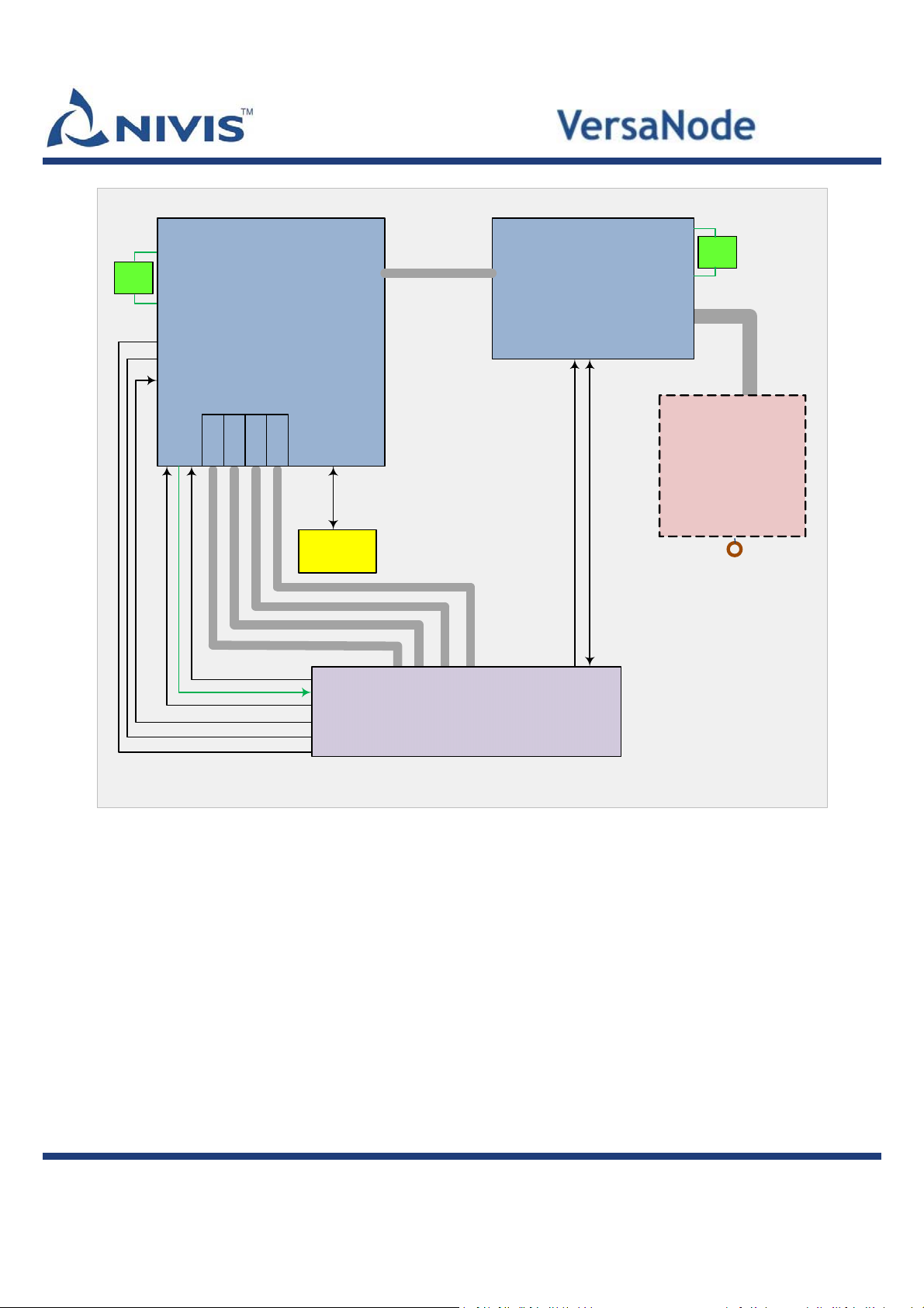
2. Pin-out and Interface Summary
The VN400 radio module uses the Freescale MC12311 SoC. Please refer to the block diagram in Figure 1 for the following
section.
The MC12311 operates in the 868 & 915 MHz ISM bands. It utilizes an internal PA (power amplifier) with a range of -20 to
+15 dBm at the antenna connector. The output power is adjustable in 1 dB steps.
The advantages of a radio module with adjustable power output are the following:
1. Ability to increase power output to +15 dBm for applications where battery consumption is not critical.
2. Enables the unit to be configured for different certification needs, especially locations that require reduced
power, such as Europe, Japan and China.
3. Provides greater power level consistency, for systems where symmetrical links are more critical.
The design of the RF section of the unit uses additional transmit components:
1. Dual LPF’s to reduce harmonic output and spurious output for regulatory compliance, such as FCC, IC, R&TTE,
and Giteki certifications.
2. Tx / Rx switch to select the transmit / receive RF path.
4. A SAW (Surface Acoustic Wave) filter is in line with the TX/RX path to significantly reduce out-of-band
interference as well as harmonic output.
As shown in the block diagram, the receive path utilizes the same Tx / Rx switch. The receive path is passive without any
additional amplification.
The Freescale SoC is clocked at 100MHz using a 15 ppm crystal, to maintain frequency stability. A 32.768 kHz real-time
clock IC is utilized to maintain SoC clocking operation during the low power / standby mode. An additional external flash
memory IC (serial) with a capacity of 2 MB is utilized for additional data storage. The Freescale Kinetis processor has the
ability to control MC12311 power and reset as needed for hibernate and low power modes.
08-00040-02.2
VN
400
Hardware
Integration Application Note
Page4/4Proprietary &
Confidential
–
NIVIS LLC
32
KHz
Freescale Kinetis Series
K60DN512ZVMC
Freescale MC Series
MC12311CHNR
30
MHz
ADC_SE13
ADC_SE12
LLWU_P13
BOOT _SW
RTC_OUT
RESET_K11
RESET_MC
BKGD
SPI
UART
I2C
JTAG
Exter nal
FLASH
UART1: TX, RX, RTS, CTS
SPI 1: CLK MOSI M ISO CS
I2C: SCL SDA
JTAG: TM S, TDO, TRST, TDI, TCL K
BOOT_SW
RTC_OUT
RESET_K11
LLWU_P13
ADC_SE12
ADC_SE13
J2 Connector
BDM: BKGD , RESET_M C
Smart Objects Radio Modem p/n: 41-00043-01 Rev. 2
RF
front-end
MMCX
Antenna Connector
08-00040-02.2
Figure 1. VN400 Functional Block Diagram
 Loading...