Harris Semiconductor LM324N, LM2902M96, LM2902M, LM2902N Datasheet

SEMICONDUCTOR
3-17
Features
• Operation from Single or Dual Supplies
• Unity-Gain Bandwidth . . . . . . . . . . . . . . . . . 1MHz (Typ)
• DC Voltage Gain . . . . . . . . . . . . . . . . . . . . . 100dB (Typ)
• Input Bias Current . . . . . . . . . . . . . . . . . . . . 45nA (Typ)
• Input Offset Voltage . . . . . . . . . . . . . . . . . . . . 2mV (Typ)
• Input Offset Current
- CA224, CA324, LM324, LM2902 . . . . . . . . . . . . 5nA (Typ)
- CA124 . . . . . . . . . . . . . . . . . . . . . . . . . . . . . 3nA (Typ)
• Replacement for Industry Types 124, 224, 324
Applications
• Summing Amplifiers
• Multivibrators
• Oscillators
• Transducer Amplifiers
• DC Gain Blocks
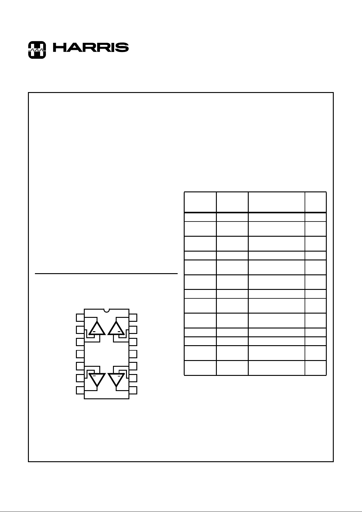
Pinout
CA124, CA224, CA324, LM2902 (PDIP, SOIC)
LM324 (PDIP)
TOP VIEW
Description
The CA124, CA224, CA324, LM324, and LM2902 consist of
four independent, high-gain operational amplifiers on a
single monolithic substrate. An on-chip capacitor in each of
the amplifiers provides frequency compensation for unity
gain. These devices are designed specially to operate from
either single or dual supplies, and the differential voltage
range is equal to the power-supply voltage. Low power drain
and an input common-mode voltage range from 0V to V+
-1.5V (single-supply operation) make these devices suitable
for battery operation.
1
2
3
4
5
6
7
14
13
12
11
10
9
8
+
1
+
4
+2+
3
OUTPUT 1
OUTPUT 2
OUTPUT 4
V-
OUTPUT 3
V+
POS.
INPUT 2
POS.
INPUT 1
NEG.
INPUT 1
NEG.
INPUT 3
POS.
INPUT 3
POS.
INPUT 4
NEG.
INPUT 4
NEG.
INPUT 2
Ordering Information
PART
NUMBER
(BRAND)
TEMP.
RANGE (oC) PACKAGE
PKG.
NO.
CA0124E -55 to 125 14 Ld PDIP E14.3
CA0124M
(124)
-55 to 125 14 Ld SOIC M14.15
CA0124M96
(124)
-55 to 125 14 Ld SOIC Tape and Reel M14.15
CA0224E -40 to 85 14 Ld PDIP E14.3
CA0224M
(224)
-40 to 85 14 Ld SOIC M14.15
CA0224M96
(224)
-40 to 85 14 Ld SOIC Tape and Reel M14.15
CA0324E 0 to 70 14 Ld PDIP E14.3
CA0324M
(324)
0 to 70 14 Ld SOIC M14.15
CA0324M96
(324)
0 to 70 14 Ld SOIC Tape and Reel M14.15
LM324N 0 to 70 14 Ld PDIP E14.3
LM2902N -40 to 85 14 Ld PDIP E14.3
LM2902M
(2902)
-40 to 85 14 Ld SOIC M14.15
LM2902M96
(2902)
-40 to 85 14 Ld SOIC Tape and Reel M14.15
November 1996
CAUTION: These devices are sensitive to electrostatic discharge. Users should follow proper IC Handling Procedures.
Copyright
© Harris Corporation 1996
File Number 796.3
CA124, CA224, CA324,
LM324, LM2902
Quad, 1MHz, Operational Amplifiers for
Commercial, Industrial, and Military Applications

3-18
CA124, CA224, CA324, LM324, LM2902
Absolute Maximum Ratings Thermal Information
Supply Voltage . . . . . . . . . . . . . . . . . . . . . . . . . . . . . . . 32V or ±16V
Differential Input Voltage. . . . . . . . . . . . . . . . . . . . . . . . . . . . . . . 32V
Input Voltage. . . . . . . . . . . . . . . . . . . . . . . . . . . . . . . . . -0.3V to 32V
Input Current (VI < -0.3V, Note 1). . . . . . . . . . . . . . . . . . . . . . .50mA
Output Short Circuit Duration (V+ ≤ 15V, Note 2). . . . . . Continuous
Operating Conditions
Temperature Range
CA124. . . . . . . . . . . . . . . . . . . . . . . . . . . . . . . . . . -55oC to 125oC
CA224, LM2902 . . . . . . . . . . . . . . . . . . . . . . . . . . . -40oC to 85oC
CA324, LM324 . . . . . . . . . . . . . . . . . . . . . . . . . . . . . .0oC to 70oC
Thermal Resistance (Typical, Note 3) θJA(oC/W)
PDIP Package. . . . . . . . . . . . . . . . . . . . . . . . . . . . . 100
SOIC Package. . . . . . . . . . . . . . . . . . . . . . . . . . . . . 175
Maximum Junction Temperature (Die) . . . . . . . . . . . . . . . . . . 175oC
Maximum Junction Temperature (Plastic Package) . . . . . . . . 150oC
Maximum Storage Temperature Range . . . . . . . . . -65oC to 150oC
Maximum Lead Temperature (Soldering 10s). . . . . . . . . . . . . 300oC
(SOIC - Lead Tips Only)
CAUTION: Stresses above those listed in “Absolute Maximum Ratings” may cause permanent damage to the device. This is a stress only rating and operation
of the device at these or any other conditions above those indicated in the operational sections of this specification is not implied
NOTES:
1. This input current will only exist when the voltage at any of the input leads is driven negative . This current is due to the collector base junction of
the input p-n-p transistors becoming forward biased and thereby acting as input diode clamps . In addition to this diode action, there is also lateral
n-p-n parasitic transistor action on the IC chip. This transistor action can cause the output v oltages of the amplifiers to go to the V+ voltage le v el
(or to ground for a large overdriv e) for the time duration that an input is driven negativ e. This transistor action is not destructive and normal output
states will re-establish when the input voltage, which was negative, again returns to a value greater than -0.3V.
2. The maximum output current is approximately 40mA independent of the magnitude of V+. Continuous short circuits at V+ > 15V can cause
excessive power dissipation and eventual destruction. Short circuits from the output to V+ can cause overheating and eventual destruction of the device.
3. θJA is measured with the component mounted on an evaluation PC board in free air.
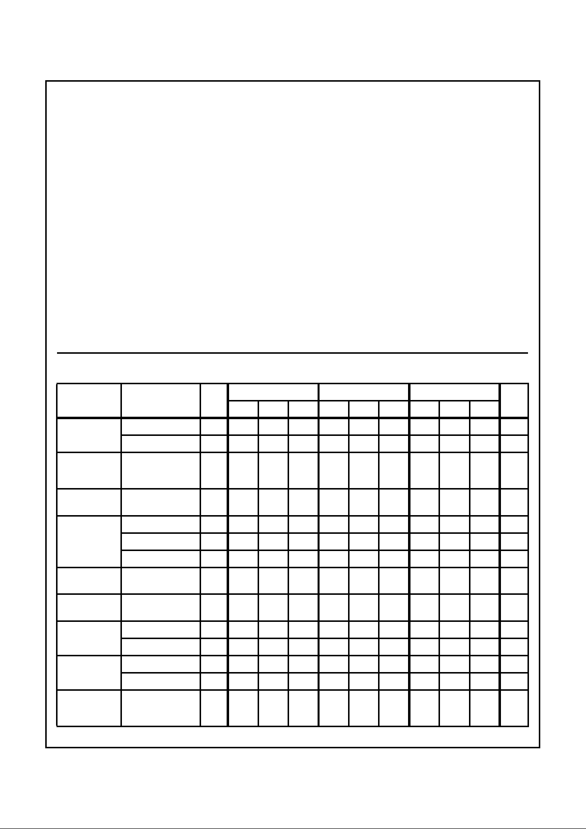
Electrical Specifications Values Apply for Each Operational Amplifier. Supply Voltage V+ = 5V, V- = 0V,
Unless Otherwise Specified
PARAMETER
TEST
CONDITIONS
TEMP.
(
o
C)
CA124 CA224, CA324, LM324 LM2902
UNITSMIN TYP MAX MIN TYP MAX MIN TYP MAX
Input Offset
Voltage (Note 6)
25-25-27---mV
Full - - 7 - - 9 - - 10 mV
Average Input
Offset Voltage
Drift
RS = 0Ω Full - 7 - - 7 - - 7 - µV/oC
Differential Input
Voltage (Note 5)
Full - - V+ - - V+ - - V+ V
Input Common
Mode Voltage
Range (Note 5)
V+ = 30V 25 0 - V+ -1.5 0 - V+ -1.5 - - - V
V+ = 30V Full 0 - V+ -2 0 - V+ -2 - - - V
V+ = 26V Full - - - - - - 0 - V+ -2 V
Common Mode
Rejection Ratio
DC 25 70 85 - 65 70 - - - - dB
Power Supply
Rejection Ratio
DC 25 65 100 - 65 100 - - - - dB
Input Bias
Current (Note 4)
II+ or II- 25 - 45 150 - 45 250 - - - nA
II+ or II- Full - - 300 - - 500 - 40 500 nA
Input Offset
Current
II+ - II- 25- 330- 550- - -nA
I
I
+ - II- Full - - 100 - - 150 - 45 200 nA
Average Input
Offset Current
Drift
Full - 10 - - 10 - - 10 - pA/oC
CA124, CA224, CA324, LM324, LM2902
 Loading...