


SEMICONDUCTOR
HIP2500
April 1997
Features
• Maximum Rating . . . . . . . . . . . . . . . . . . . . . . . . 500V
• Ability to Interface and Drive N-Channel Power
Devices
• Floating Bootstrap Power Supply for Upper Rail
Drive
• CMOS Schmitt-Triggered Inputs with Hysteresis
and Pull-Down
• Up to 400kHz Operation
• Single Low Current Bias Supply
• Latch-Up Immune CMOS Logic
• Peak Drive. . . . . . . . . . . . . . . . . . . . . . . . . .Up to 2.0A
o
• Gate Drive Rise Time (+125
C). . . . . . . < 25ns (Typ)
Applications
• High Frequency Switch-Mode Power Supply
• Induction Heating and Welding
• Switch Mode Amplifiers
• AC and DC Motor Drives
• Electronic Lamp Ballasts
• Battery Chargers
• UPS Inverters
• Noise Cancellation in Amplifier Systems
Ordering Information
Half Bridge 500VDC Driver
Description
The HIP2500 is a high voltage integrated circuit (HVIC) optimized
to drive N-Channel MOS gated power devices in half bridge topologies. It provides the necessary control for PWM motor drive,
power supply, and UPS applications. The SD pin allows external
shutdown of gate drive to both upper and lower gate outputs. Undervoltage lockout will not allow gating when the bias voltage is too
low to drive the external switches into satur ation.
The HIP2500IP is pin and function compatible to the International Rectifier IR2110. The HIP2500 has superior ability to
accept negative voltages from the V
forward recovery of the lower flyback diode.
The HIP2500IB is a SOIC or small outline IC form of the
HIP2500. The HIP2500IB drives high side and low side referenced power switches just like the HIP2500IP.
The HIP2500IP1 is a 16 lead Plastic DIP form of the HIP2500.
Pins 4 and 5 removed from lead frame to provide extra creepage and strike distances in high voltage applications.
Please see Application Note AN9010 for more information.
Functional Block Diagram
HIP2500
V
HIN
DD
UV
LEVEL
SHIFT
pin to the COM pin due to
S
S
LATCH
R
DRIVER
V
HO
V
B
S
PART
NUMBER
HIP2500IP -40 to +85 14 Ld PDIP E14.3
HIP2500IP1 -40 to +85 16 Ld PDIP E16.3
HIP2500IB -40 to +85 16 Ld SOIC (W) M16.3
TEMP.
RANGE (oC) PACKAGE PKG NO.
V
SD
LOGIC
LIN
SS
Pinouts
HIP2500 (PDIP)
TOP VIEW
LO
1
2
COM
V
3
CC
4
NC
V
5
S
V
B
6
HO
7
CAUTION: These devices are sensitive to electrostatic discharge. Users should follow proper I.C. Handling Procedures.
Copyright
© Harris Corporation 1997
14
NC
V
13
SS
LIN
12
11
SD
10
HIN
9
V
DD
NC
8
COM
V
LO
CC
NC
NC
V
V
HO
1
2
3
4
5
6
S
7
B
8
HIP2500 (SOIC)
TOP VIEW
1
16
NC
15
V
SS
14
LIN
13
SD
12
HIN
11
V
DD
10
NC
9
NC
COM
V
LO
CC
V
V
HO
1
2
3
6
S
7
B
8
UV
DRIVER
HIP2500 (PDIP)
TOP VIEW
File Number
16
15
14
13
12
11
10
9
V
CC
LO
COM
NC
V
SS
LIN
SD
HIN
V
DD
NC
NC
2801.8
HIP2500
Absolute Maximum Ratings Full Temperature Range Unless
Otherwise Noted, All Voltages Referenced to V
Floating Supply Voltage, VB . . . . . . . . . . . . . . .VS-0.5V to VS+18.0V
(Positive Terminal)
Floating Supply Voltage, VS . . . . . . . . . . . . . . . . . . . . . . . . . . . 500V
(Common Terminal)
High Side Channel Output Voltage, VHO . . . . . . . .-0.5V to VB+0.5V
Fixed Supply Voltage, VCC. . . . . . . . . . . . . . . . . . . . . -0.5V to 18.0V
Low Side Channel Output Voltage, VLO. . . . . . . .-0.5V to VCC+0.5V
Logic Supply Voltage, VDD . . . . . . . . . . . . . . . . . . . . . -0.5V to 18.0V
Unless Otherwise Noted.
SS
Thermal Information
Thermal Resistance (Note 1, Typical) θ
HIP2500IP. . . . . . . . . . . . . . . . . . . . . . . . . . . . . . . . 75oC/W
HIP2500IP1. . . . . . . . . . . . . . . . . . . . . . . . . . . . . . . 80oC/W
HIP2500IB. . . . . . . . . . . . . . . . . . . . . . . . . . . . . . . . 90oC/W
See Maximum Power Dissipation vs Temperature Curve
Junction Temperature Range . . . . . . . . . . . . . . . . .-40oC to +125oC
Storage Temperature Range, TS. . . . . . . . . . . . . . .-40oC to +150oC
Operating Ambient Temperature Range, TA . . . . . . .-40oC to +85oC
JA
Logic Input Voltage, VIN . . . . . . . . . . . . . . . . . . . .-0.5V to VDD+0.5V
[HIN, LIN & SD (Shutdown)]
VDD to COM and VCC to VSS Voltage. . . . . . . . . . . . . -0.5V to 18.0V
NOTE:
1. θJA is measured with the component mounted on an evaluation PC board in free air.
CAUTION: Stresses above those listed in “Absolute Maximum Ratings” may cause permanent damage to the device. This is a stress only rating and operation
of the device at these or any other conditions above those indicated in the operational sections of this specification is not implied.
Recommended DC Operating Conditions
Floating Supply Voltage, VB . . . . . . . . . . . . . . . . VS+10V to VS+15V
(Floating Terminal)
High Side Channel Output Voltage, VHO . . . . . . . . . . . . . .10V to V
(With Respect to VS)
Fixed Supply Voltage, VCC. . . . . . . . . . . . . . . . . . . . . . . .10V to 15V
Electrical Specifications V
= (VB- VS) = VDD = 15V, COM = VSS = 0, Unless Otherwise Noted
CC
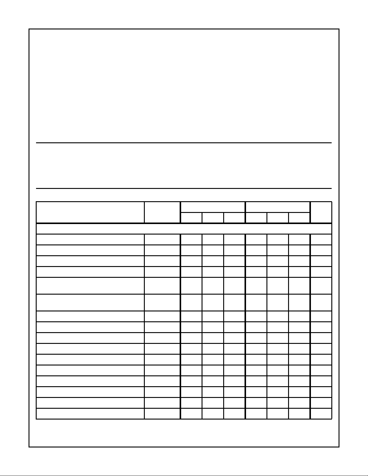
PARAMETER SYMBOL MIN TYP MAX MIN TYP MAX UNITS
Low Side Channel Output Voltage, VLO . . . . . . . . . . . . . . 0V to V
Logic Supply Voltage, VDD . . . . . . . . . . . . . . . . . . . . . . . . 4V to V
Floating Supply Voltage, VS . . . . . . . . . . . . . . . . . . . . -4.0V to 500V
B
(Common Terminal)
VSS and COM potentials to be equal.
= +25oCT
T
J
= -40oC TO +125oC
J
CC
CC
DC CHARACTERISTICS
Quiescent VCC Current I
Quiescent VBS Current I
Quiescent VDD Current I
QCC
QBS
QDD
- 1.5 1.9 - - 2.0 mA
- 300 400 - 300 435 µA
- 0.1 1 - - 1.8 µA
Quiescent Leakage Current IS (500V) - 0.4 3.0 - - - µA
Logic Input Pulldown Current, VIN = V
DD
IN+ -1220- -22µA
(HIN, LIN, SD)
Logic Input Leakage Current, VIN = V
SS
IN- - 0 1 - 0 1 µA
(HIN, LIN, SD)
Logic Input Positive Going Threshold (Note 2) VTH+ 7.5 8.0 8.5 7.5 8.0 8.6 V
Logic Input Negative Going Threshold (Note 2) VTH- 5.5 5.9 6.3 5.5 5.9 6.4 V
Undervoltage Positive Going Threshold UV+ 8.0 9.35 9.99 7.8 - 9.99 V
Undervoltage Negative Going Threshold UV- 7.7 9.05 9.69 7.5 - 9.69 V
Undervoltage Hysteresis (VCC) UVHYS (VCC) 250 - 450 170 - 530 mV
Undervoltage Hysteresis (VBS) UVHYS (VBS) 250 - 450 170 - 530 mV
Output High Open Circuit Voltage (HO, LO) V
Output Low Open Circuit Voltage (HO, LO) V
Output High Short Circuit Current (Sourcing) I
Output Low Short Circuit Current (Sinking) I
+ 14.95 15 - 14.95 15 - V
OUT
- - - 0.05 - - 0.05 V
OUT
+ 1.65 2.1 - 1.15 1.6 - A
OUT
- 1.85 2.3 - 1.35 1.7 - A
OUT
NOTE:
2. See Figure 8 for logic supply voltages other than 15.0V.
2

Switching Specifications
HIP2500
PARAMETER SYMBOL
HIGH SIDE CHANNEL WITH 500V OFFSET, CL = 1000pF
High Side Turn-On Propagation Delay t
High Side Turn-Off Propagation Delay t
OFF
High Side Rise Time t
High Side Turn-Off Fall Time t
LOW SIDE CHANNEL, CL = 1000pF
Low Side Turn-On Propagation Delay t
Low Side Turn-Off Propagation Delay t
OFF
Low Side Turn-On Rise Time t
Low Side Turn-Off Fall Time t
Shutdown Propagation Delay
t
High Side Shutdown
Low Side Shutdown
SDHO
t
SDLO
HIGH SIDE CHANNEL WITH 500V OFFSET, CL = 1000pF
Turn-On Propagation Delay Matching
(Between HO and LO)
ON
ON
M
TJ = +25oCT
= -40oC TO +125oC
J
UNITSMIN TYP MAX MIN TYP MAX
320 420 525 230 - 725 ns
260 385 450 190 - 625 ns
R
F
- 25 50 - 25 50 ns
- 25 50 - 25 50 ns
250 365 450 190 - 600 ns
175 295 370 125 - 475 ns
R
F
- 25 50 - 30 50 ns
- 25 50 - 30 50 ns
300 400 490 200 - 650 ns
175 320 400 125 - 500 ns
t
0 - 125 0 - 185 ns
Minimum On Output Pulse Width (HO, LO) PW
Minimum Off Output Pulse Width (HO, LO) PW
Minimum On Input Pulse Width (HIN, LIN) PW
Minimum Off Input Pulse Width (HIN, LIN) PW
OUT(MIN)
OUTMIN
ON(MIN)
OFF(MIN)
Deadtime LO Turn-Off to HO Turn-On DHt
Deadtime HO Turn-Off to LO Turn-On DLt
ON
ON
- 35 50 - 35 55 ns
275 440 640 250 440 650 ns
- 100 145 - 100 175 ns
- 110 200 - 110 220 ns
- 125 - - 125 - ns
- -20 - - -20 - ns
MAXIMUM TRANSIENT CONDITIONS
Offset Supply Operating Transient dVS/dt - - 50 - - 50 V/ns
Logic Truth Table
HIN LIN UV
H
0000000Normal Off
0100001Lower On
1000010Upper On
1100011Both On
XXXX100Chip Disabled
XX11X00V
X110001V
1X01010V
UV
L
SD HO LO COMMENTS
UV Lockout and VBS Lockout
CC
UV Lockout
BS
UV Lockout
CC
3

Typical Performance Curves
HIP2500
2.5
2.25
2
1.75
1.5
1.25
1
0.75
0.5
0.25
MAXIMUM POWER DISSIPATION (W)
0
-40-30 -20 -10 0 10 20 30 40 50 60 70 80 90 100110120130
HIP2500-IP
HIP2500-IP1
HIP2500-IB
AMBIENT TEMPERATURE (oC)
FIGURE 1. MAXIMUM POWER DISSIPATION vs TEMPERATURE
10
VS = VSS = COM
V
= VCC = 15V
1.0
BS
TA = +25oC
DC
1.0
V
= 15V
BIAS
= 100pF
C
L
T
= +25oC
A
0.1
0.01
0.001
HIGH VOLTAGE POWER DISSIPATION (W)
10 100 1000
SWITCHING FREQUENCY (kHz)
VS = 400V
V
S
V
S
V
S
FIGURE 2. HIGH VOLTAGE POWER DISSIPATION vs
SWITCHING FREQUENCY
6
MAX VSS OFFSET
4
2
= 300V
= 200V
= 100V
0.1
POWER DISSIPATION (W)
0.01
10 100 1000
SWITCHING FREQUENCY (kHz)
2100pF
907pF
100pF
NOTE: All switching losses assumed to be in IC.
FIGURE 3. LOW VOLTAGE POWER DISSIPATION vs
FREQUENCY
10
500V
400V
300V
1.0
CURRENT (µA)
OFFSET SUPPLY LEAKAGE
0.1
0 20 40 60 80 100 120 140
TEMPERATURE (oC)
FIGURE 5. OFFSET SUPPLY LEAKAGE vs TEMPERATURE
200V
100V
0
LOGIC SUPPLY
OFFSET VOLTAGE (V)
-2
MIN VSS OFFSET
-4
FIGURE 4. V
10
OFFSET VOLTAGE (NEGATIVE)
S
MAX V
10 12 14 16
SUPPLY VOLTAGE (V)
OFFSET vs VCC SUPPLY VOLTAGE
SS
VCC = 15V AND 12V
9
= +25oC
T
J
8
7
VCC = 15V
6
5
4
3
2
10 11 12 13 14 15 16 17 18
BOOTSTRAP SUPPLY VOLTAGE
VCC = 12V
FIGURE 6. MAXIMUM NEGATIVE VS OFFSET VOLTAGE vs V
VOLTAGE
BS
4

HIP2500
Typical Performance Curves
9.35
9.3
9.25
9.2
9.15
9.1
9.05
9.0
8.95
UNDERVOLTAGE LOCKOUT (V)
8.9
-40 0 40 100 140
TEMPERATURE (
(Continued)
VBS UV-
o
C)
VCC UV+
VBS UV+
VCC UV-
120806020-20
10
TJ = -40oC TO +125oC
8
6
4
LOGIC THRESHOLD (V)
2
6 8 10 12 14 16 18
5
LOGIC SUPPLY VOLTAGE (V)
VTH+
(V
TO VSS)
DD
VTH-
FIGURE 7. UNDERVOLTAGE LOCKOUT vs TEMPERATURE FIGURE 8. INPUT LOGIC THRESHOLD vs SUPPLY VOLTS
450
18V IQBS1
400
350
300
250
SUPPLY CURRENT (µA)
BS
200
V
150
-50 0 50 100 150
JUNCTION TEMPERATURE (
18V IQBS0
14V IQBS1
14V IQBS0
10V IQBS1
10V IQBS0
o
C)
120
100
80
60
40
t
R
20
RISE AND FALL TIMES (ns)
t
F
0
100 1000 1E4
LOAD CAPACITANCE (pF)
FIGURE 9. QUIESCENT VBS SUPPLY CURRENT vs
FIGURE 10. RISE AND FALL TIME vs LOAD CAPACITANCE
TEMPERATURE
3.0
2.5
2.0
1.5
1.0
0.5
PEAK OUTPUT CURRENT (A)
0
-40
0
25
125
-40
0
25
125
0246810121416
SOURCE/SINK DRAIN-SOURCE VOLTAGE
SOURCE DRIVER
SINK DRIVER
30
28
26
24
22
20
18
16
14
RISE AND FALL TIME (ns)
12
10
-50 0 50 100 150
TEMPERATURE (
o
C)
FIGURE 11. DRIVER SINK/SOURCE V-I CHARACTERISTIC FIGURE 12. RISE AND FALL TIME vs TEMPERATURE
t
F
t
R
5
HIP2500
Typical Performance Curves
(Continued)
30
28
26
t
F
24
22
20
18
t
R
16
14
RISE AND FALL TIME (ns)
12
10
10 11 12 13 14 15 16
SUPPLY VOLTAGE (V)
FIGURE 13. RISE AND FALL TIME vs SUPPLY VOLTAGE
700
600
500
460
440
Ht
ON
420
Ht
400
OFF
380
Lt
360
ON
340
PROPAGATION DELAY (ns)
320
300
10 11 12 13 14 15 16
Lt
OFF
SUPPLY VOLTAGE (V)
FIGURE 14. PROPAGATION DELAY vs SUPPLY VOLTAGE
Ht
ON
Ht
OFF
Lt
ON
400
300
PROPAGATION DELAY (ns)
200
FIGURE 15. PROPAGATION DELAYS AT VCC = 15V
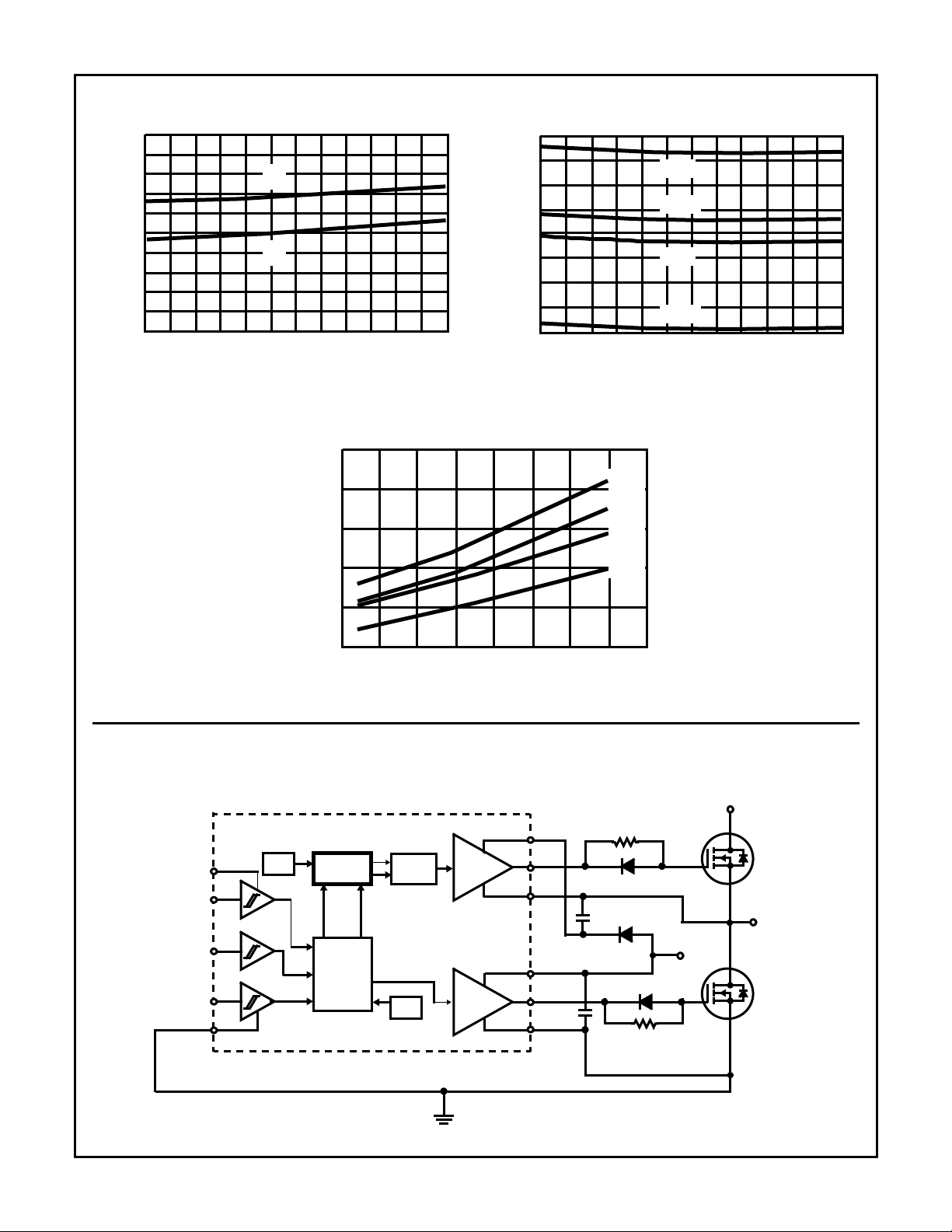
Typical Application Diagram
HIP2500
V
HIN
LIN
V
DD
SD
SS
UV
LEVEL
SHIFT
LOGIC
Lt
OFF
-50 0 50 100 150
JUNCTION TEMPERATURE (
S
LATCH
DRIVER
R
UV
DRIVER
V
HO
V
V
LO
CC
o
C)
R
B
S
G
D
F
C
F
COM
R
H
V
TO
LOAD
V
CC
G
6
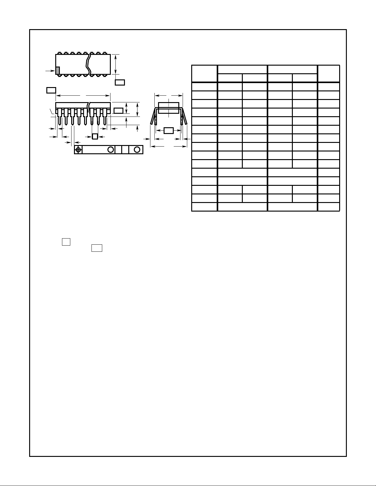
Dual-In-Line Plastic Packages (PDIP)
HIP2500
N
D1
-C-
E1
-B-
A1
A2
A
L
e
C
S
INDEX
AREA
BASE
PLANE
SEATING
PLANE
D1
B1
1 2 3 N/2
-AD
e
B
0.010 (0.25) C AMB
NOTES:
1. Controlling Dimensions: INCH. In case of conflict between
English and Metric dimensions, the inch dimensions control.
2. Dimensioning and tolerancing per ANSI Y14.5M-1982.
3. Symbols are defined in the “MO Series Symbol List” in Section
2.2 of Publication No. 95.
4. Dimensions A, A1 and L are measured with the package seated
in JEDEC seating plane gauge GS-3.
5. D, D1, and E1 dimensions do not include mold flash or protrusions. Mold flash or protrusions shall not exceed 0.010 inch
(0.25mm).
6. E and are measured with the leads constrained to be per-
e
pendicular to datum .
A
-C-
7. eB and eC are measured at the lead tips with the leads unconstrained. eC must be zero or greater.
8. B1 maximum dimensions do not include dambar protrusions.
Dambar protrusions shall not exceed 0.010 inch (0.25mm).
9. N is the maximum number of terminal positions.
10. Corner leads (1, N, N/2 and N/2 + 1) for E8.3, E16.3, E18.3,
E28.3, E42.6 will have a B1 dimension of 0.030 - 0.045 inch
(0.76 - 1.14mm).
E14.3 (JEDEC MS-001-AA ISSUE D)
14 LEAD DUAL-IN-LINE PLASTIC PACKAGE
INCHES MILLIMETERS
SYMBOL
A - 0.210 - 5.33 4
E
A1 0.015 - 0.39 - 4
A2 0.115 0.195 2.93 4.95 -
B 0.014 0.022 0.356 0.558 -
C
L
e
A
C
e
B
B1 0.045 0.070 1.15 1.77 8
C 0.008 0.014 0.204 0.355 D 0.735 0.775 18.66 19.68 5
D1 0.005 - 0.13 - 5
E 0.300 0.325 7.62 8.25 6
E1 0.240 0.280 6.10 7.11 5
e 0.100 BSC 2.54 BSC -
e
A
e
B
0.300 BSC 7.62 BSC 6
- 0.430 - 10.92 7
L 0.115 0.150 2.93 3.81 4
N14 149
NOTESMIN MAX MIN MAX
Rev. 0 12/93
7

Dual-In-Line Plastic Packages (PDIP)
HIP2500
N
D1
-C-
E1
-B-
A1
A2
A
L
e
C
S
INDEX
AREA
BASE
PLANE
SEATING
PLANE
D1
B1
1 2 3 N/2
-AD
e
B
0.010 (0.25) C AMB
NOTES:
1. Controlling Dimensions: INCH. In case of conflict between
English and Metric dimensions, the inch dimensions control.
2. Dimensioning and tolerancing per ANSI Y14.5M-1982.
3. Symbols are defined in the “MO Series Symbol List” in Section
2.2 of Publication No. 95.
4. Dimensions A, A1 and L are measured with the package seated
in JEDEC seating plane gauge GS-3.
5. D, D1, and E1 dimensions do not include mold flash or protrusions. Mold flash or protrusions shall not exceed 0.010 inch
(0.25mm).
6. E and are measured with the leads constrained to be per-
e
pendicular to datum .
A
-C-
7. eB and eC are measured at the lead tips with the leads unconstrained. eC must be zero or greater.
8. B1 maximum dimensions do not include dambar protrusions.
Dambar protrusions shall not exceed 0.010 inch (0.25mm).
9. N is the maximum number of terminal positions.
10. Corner leads (1, N, N/2 and N/2 + 1) for E8.3, E16.3, E18.3,
E28.3, E42.6 will have a B1 dimension of 0.030 - 0.045 inch
(0.76 - 1.14mm).
E16.3 (JEDEC MS-001-BB ISSUE D)
16 LEAD DUAL-IN-LINE PLASTIC PACKAGE
INCHES MILLIMETERS
SYMBOL
A - 0.210 - 5.33 4
E
A1 0.015 - 0.39 - 4
A2 0.115 0.195 2.93 4.95 -
B 0.014 0.022 0.356 0.558 -
C
L
e
A
C
e
B
B1 0.045 0.070 1.15 1.77 8, 10
C 0.008 0.014 0.204 0.355 D 0.735 0.775 18.66 19.68 5
D1 0.005 - 0.13 - 5
E 0.300 0.325 7.62 8.25 6
E1 0.240 0.280 6.10 7.11 5
e 0.100 BSC 2.54 BSC -
e
A
e
B
0.300 BSC 7.62 BSC 6
- 0.430 - 10.92 7
L 0.115 0.150 2.93 3.81 4
N16 169
NOTESMIN MAX MIN MAX
Rev. 0 12/93
8
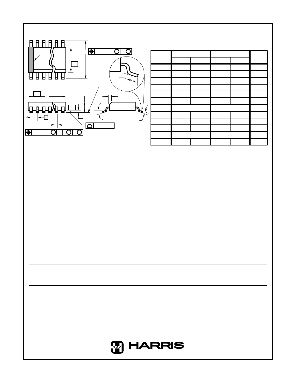
Small Outline Plastic Packages (SOIC)
HIP2500
N
INDEX
AREA
123
-AD
e
B
0.25(0.010) C AMB
E
SEATING PLANE
-C-
M
H
-B-
A
A1
S
0.25(0.010) B
α
0.10(0.004)
M
L
h x 45
M
o
NOTES:
1. Symbols are defined in the “MO Series Symbol List” in Section
2.2 of Publication Number 95.
2. Dimensioning and tolerancing per ANSI Y14.5M-1982.
3. Dimension “D” does not include mold flash, protrusions or gate
burrs. Mold flash, protrusion and gate burrs shall not exceed
0.15mm (0.006 inch) per side.
4. Dimension “E” does not include interlead flash or protrusions. Interlead flash and protrusions shall not exceed 0.25mm (0.010
inch) per side.
5. The chamfer on the body is optional. If it is not present, a visual
index feature must be located within the crosshatched area.
6. “L” is the length of terminal for soldering to a substrate.
7. “N” is the number of terminal positions.
8. Terminal numbers are shown for reference only.
9. The lead width “B”, as measured 0.36mm (0.014 inch) or greater
above the seating plane, shall not exceed a maximum value of
0.61mm (0.024 inch)
10. Controlling dimension: MILLIMETER. Converted inch dimensions are not necessarily exact.
M16.3 (JEDEC MS-013-AA ISSUE C)
16 LEAD WIDE BODY SMALL OUTLINE PLASTIC PACKAGE
INCHES MILLIMETERS
SYMBOL
A 0.0926 0.1043 2.35 2.65 -
A1 0.0040 0.0118 0.10 0.30 -
B 0.013 0.0200 0.33 0.51 9
C 0.0091 0.0125 0.23 0.32 D 0.3977 0.4133 10.10 10.50 3
E 0.2914 0.2992 7.40 7.60 4
e 0.050 BSC 1.27 BSC H 0.394 0.419 10.00 10.65 -
C
h 0.010 0.029 0.25 0.75 5
L 0.016 0.050 0.40 1.27 6
N16 167
o
α
0
o
8
o
0
NOTESMIN MAX MIN MAX
o
8
-
Rev. 0 12/93
Harris Semiconductor products are sold by description only. Harr is Semiconductor reserves the right to make changes in circuit design and/or specifications at
any time without notice. Accordingly, the reader is cautioned to verify that data sheets are current before placing orders. Information furnished by Harris is
believed to be accurate and reliable. However, no responsibility is assumed by Harris or its subsidiaries for its use; nor for any infringements of patents or other
rights of third parties which may result from its use. No license is granted by implication or otherwise under any patent or patent rights of Harris or its subsidiaries.
Sales Office Headquarters
For general information regarding Harris Semiconductor and its products, call 1-800-4-HARRIS
UNITED STATES
Harris Semiconductor
P. O. Box 883, Mail Stop 53-210
Melbourne, FL 32902
TEL: 1-800-442-7747
(407) 729-4984
FAX: (407) 729-5321
EUROPE
Harris Semiconductor
Mercure Center
100, Rue de la Fusee
1130 Brussels, Belgium
TEL: (32) 2-724-2111
SOUTH ASIA
Harris Semiconductor H.K. Ltd.
13/F Fourseas Building
208-212 Nathan Road
Tsimshatsui, Kowloon
Hong Kong
TEL: (852) 723-6339
SEMICONDUCTOR
9
NORTH ASIA
Harris K.K.
Kojimachi-Nakata Bldg. 4F
5-3-5 Kojimachi
Chiyoda-ku, Tokyo 102 Japan
TEL: (81) 3-3265-7571
TEL: (81) 3-3265-7572 (Sales)
 Loading...