

Harris Semiconductor HIN241IB, HIN241CB, HIN241BY, HIN240IN, HIN238CP Datasheet
...
SEMICONDUCTOR
8-29
August 1997
HIN230 thru HIN241
+5V Powered RS-232 Transmitters/Receivers
Features
• Meets All RS-232E and V.28 Specifications
• Requires Only Single +5V Power Supply
- (+5V and +12V - HIN231 and HIN239)
• HIN233 and HIN235 Require No External Capacitors
• Onboard Voltage Doubler/Inverter
• Low Power Consumption
• Low Power Shutdown Function
• Three-State TTL/CMOS Receiver Outputs
• Multiple Drivers
- ±10V Output Swing for +5V lnput
- 300Ω Power-Off Source Impedance
- Output Current Limiting
- TTL/CMOS Compatible
- 30V/µs Maximum Slew Rate
• Multiple Receivers
- ±30V Input Voltage Range
-3kΩ to 7kΩ Input Impedance
- 0.5V Hysteresis to Improve Noise Rejection
Description
The HIN230-HIN241 family of RS-232 transmitters/receivers
interface circuits meet all ElA RS-232E and V.28 specifications,
and are particularly suited for those applications where ±12V is
not available. They require a single +5V power supply (except
HIN231 and HIN239) and features onboard charge pump voltage converters which generate +10V and -10V supplies from
the 5V supply. The HIN233 and HIN235 require no external
capacitors and are ideally suited for applications where circuit
board space is critical. The family of devices offer a wide v ariety
of RS-232 transmitter/receiver combinations to accommodate
various applications (see Selection Table).
The drivers feature true TTL/CMOS input compatibility, slewrate-limited output, and 300Ω power-off source impedance.
The receivers can handle up to ±30V, and have a 3kΩ to 7kΩ
input impedance. The receivers also feature hysteresis to
greatly improve noise rejection.
Applications
• Any System Requiring RS-232 Communications Port
- Computer - Portable, Mainframe, Laptop
- Peripheral - Printers and Terminals
- Instrumentation
- Modems
Selection Table
PART
NUMBER
POWER SUPPLY
VOLTAGE
NUMBER OF
RS-232
DRIVERS
NUMBER OF
RS-232
RECEIVERS
EXTERNAL
COMPONENTS
LOW POWER
SHUTDOWN/TTL
THREE-ST ATE
NUMBER OF
LEADS
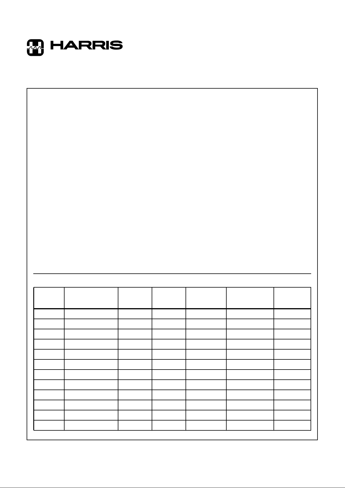
HIN230 +5V 5 0 4 Capacitors YES/NO 20
HIN231 +5V and +7.5V to 13.2V 2 2 2 Capacitors NO/NO 16
HIN232 +5V 2 2 4 Capacitors NO/NO 16
HIN233 +5V 2 2 None NO/NO 20
HIN234 +5V 4 0 4 Capacitors NO/NO 16
HIN235 +5V 5 5 None YES/YES 24
HIN236 +5V 4 3 4 Capacitors YES/YES 24
HIN237 +5V 5 3 4 Capacitors NO/NO 24
HIN238 +5V 4 4 4 Capacitors NO/NO 24
HIN239 +5V and +7.5V to 13.2V 3 5 2 Capacitors NO/YES 24
HIN240 +5V 5 5 4 Capacitors YES/YES 44
HIN241 +5V 4 5 4 Capacitors YES/YES 28
CAUTION: These devices are sensitive to electrostatic discharge. Users should follow proper IC Handling Procedures.
Copyright
© Harris Corporation 1997
File Number 3138.4
8-30
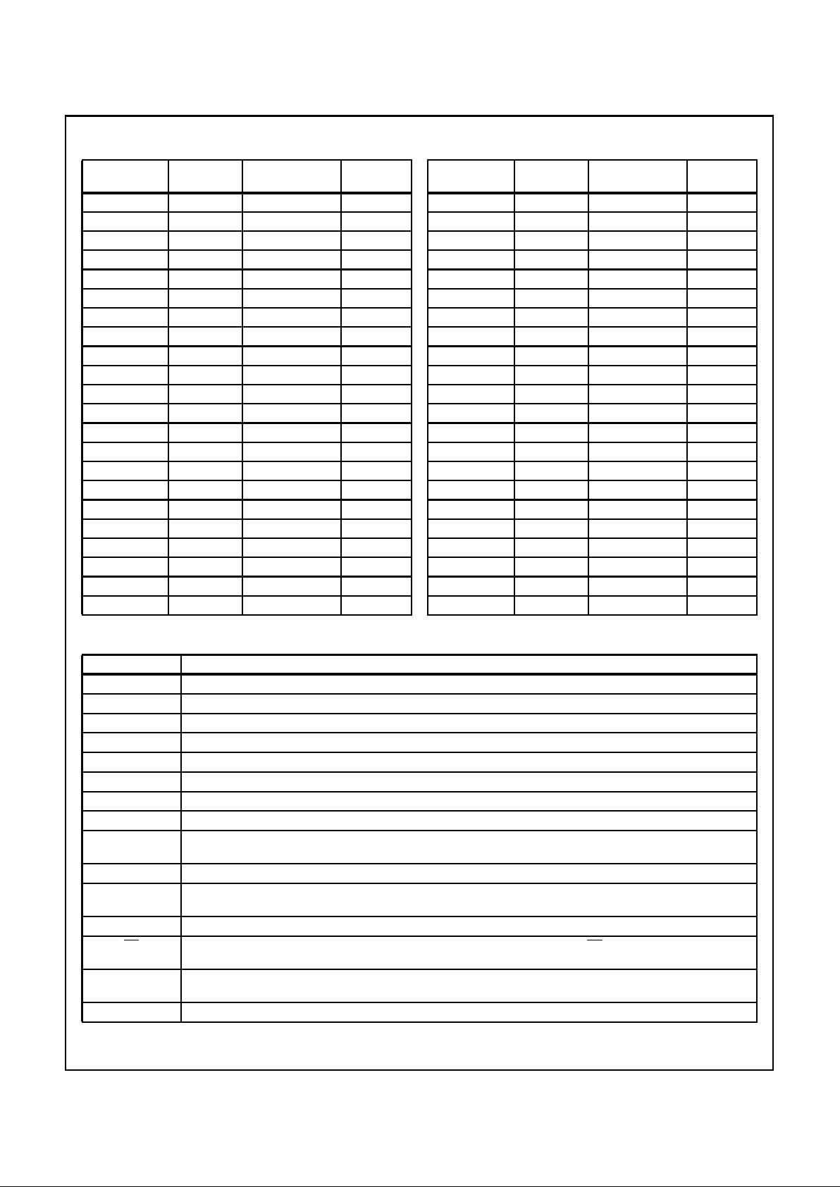
Ordering Information
Pin Descriptions
PART
NUMBER
TEMP.
RANGE (oC) PACKAGE PKG. NO.
HIN230CB 0 to 70 20 Ld SOIC M20.3
HIN230IB -40 to 85 20 Ld SOIC M20.3
HIN230BY Die
HIN231CB 0 to 70 16 Ld SOIC M16.3
HIN231IB -40 to 85 16 Ld SOIC M16.3
HIN231BY Die
HIN232CP 0 to 70 16 Ld PDIP E16.3
HIN232CB 0 to 70 16 Ld SOIC M16.3
HIN232IP -40 to 85 16 Ld PDIP E16.3
HIN232IJ -40 to 85 16 Ld CERDIP F16.3
HIN232IB -40 to 85 16 Ld SOIC M16.3
HIN232MJ -55 to 125 16 Ld CERDIP F16.3
HIN232BY Die
HIN233CP 0 to 70 20 Ld PDIP E20.3
HIN234CB 0 to 70 16 Ld SOIC M16.3
HIN234IB -40 to 85 16 Ld SOIC M16.3
HIN234BY Die
HIN235CP 0 to 70 24 Ld PDIP E24.3
HIN236CP 0 to 70 24 Ld PDIP E24.3
HIN236CB 0 to 70 24 Ld SOIC M24.3
HIN236IP -40 to 85 24 Ld PDIP E24.3
HIN236IB -40 to 85 24 Ld SOIC M24.3
HIN236BY Die
HIN237CP 0 to 70 24 Ld PDIP E24.3
HIN237CB 0 to 70 24 Ld SOIC M24.3
HIN237IP -40 to 85 24 Ld PDIP E24.3
HIN237IB -40 to 85 24 Ld SOIC M24.3
HIN237BY Die
HIN238CP 0 to 70 24 Ld PDIP E24.3
HIN238CB 0 to 70 24 Ld SOIC M24.3
HIN238IP -40 to 85 24 Ld PDIP E24.3
HIN238IB -40 to 85 24 Ld SOIC M24.3
HIN238BY Die
HIN239CB 0 to 70 24 Ld SOIC M24.3
HIN239IB -40 to 85 24 Ld SOIC M24.3
HIN239BY Die
HIN240CN 0 to 70 44 Ld MQFP Q44.10X10
HIN240IN -40 to 85 44 Ld MQFP Q44.10X10
HIN240BY Die
HIN241CB 0 to 70 28 Ld SOIC M28.3
HIN241IB -40 to 85 28 Ld SOIC M28.3
HIN241CA 0 to 70 28 Ld SSOP M28.209
HIN241IA -40 to 85 28 Ld SSOP M28.209
HIN241BY Die
PART
NUMBER
TEMP.
RANGE (oC) PACKAGE PKG. NO.
PIN FUNCTION
V
CC
Power Supply Input 5V ±10%. HIN233 and HIN235 5V ±5%.
V+ Internally generated positive supply (+10V nominal), HIN231 and HIN239 requires +7.5V to +13.2V.
V- Internally generated negative supply (-10V nominal).
GND Ground lead. Connect to 0V.
C1+ External capacitor (+ terminal) is connected to this lead.
C1- External capacitor (- terminal) is connected to this lead.
C2+ External capacitor (+ terminal) is connected to this lead.
C2- External capacitor (- terminal) is connected to this lead.
T
IN
Transmitter Inputs. These leads accept TTL/CMOS levels. An internal 400kΩ pull-up resistor to VCCis
connected to each lead.
T
OUT
Transmitter Outputs. These are RS-232 levels (nominally ±10V).
R
IN
Receiver Inputs. These inputs accept RS-232 input levels. An internal 5kΩ pull-down resistor to GND is connected
to each input.
R
OUT
Receiver Outputs. These are TTL/CMOS levels.
EN Enable input. This is an active low input which enables the receiver outputs. With EN = 5V, the outputs are placed
in a high impedance state.
SD Shutdown Input. With SD = 5V, the charge pump is disabled, the receiver outputs are in a high impedance state and
the transmitters are shut off.
NC No Connect. No connections are made to these leads.
HIN230 thru HIN241
8-31
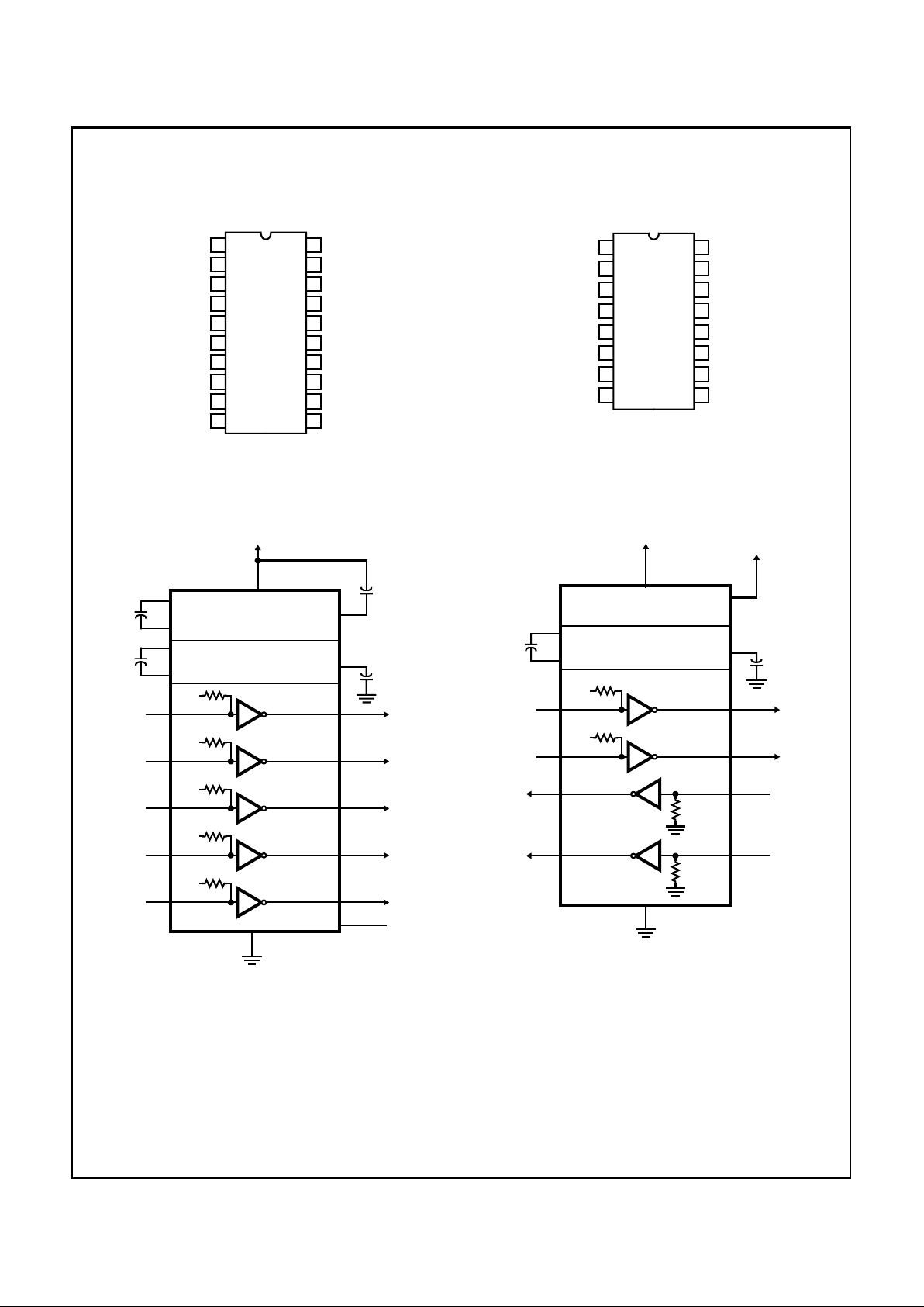
Pinouts
HIN230 (SOIC)
TOP VIEW
HIN231 (SOIC)
TOP VIEW
T3
OUT
T1
OUT
T2
OUT
T2
IN
T1
IN
GND
C1+
V
CC
V+
C1-
T4
OUT
NC
SHUTDOWN
T5
OUT
T5
IN
T4
IN
T3
IN
VC2C2+
11
12
13
14
15
16
17
18
20
19
10
9
8
7
6
5
4
3
2
1
14
15
16
9
13
12
11
10
1
2
3
4
5
7
6
8
C+
C-
V-
T2
OUT
R2
IN
NC
T2
IN
V+
GND
T1
OUT
R1
IN
R1
OUT
T1
IN
NC
V
CC
R2
OUT
V
CC
+5V TO 10V
VOLTAGE DOUBLER
+10V TO -10V
VOLTAGE INVERTER
T1
OUT
T2
OUT
T3
OUT
T4
OUT
T5
OUT
T5
IN
T4
IN
T1
IN
T2
IN
T3
IN
T1
T2
T3
T4
T5
+5V
400kΩ
+5V
+
1µF
+
1µF
+
1µF
5
4
2
3
14 1
15 20
1619
8
10
9
13
V+
V-
C1+
C1C2+
C2-
17
SHUTDOWN
7
+5V
400kΩ
+5V
400kΩ
+5V
400kΩ
+5V
400kΩ
+
1µF
11
12
6
V
CC
+5V
16
V+
+7.5V TO +13.2V
15
T1
OUT
T2
OUT
T1
IN
T2
IN
T1
T2
10
7
13
4
+5V
400kΩ
+5V
400kΩ
R1
OUT
R1
IN
R1
1211
5kΩ
R2
OUT
R2
IN
R2
56
5kΩ
+12V TO -12V
VOLTAGE INVERTER
1µF
3
V-
C+
C-
+
1µF
1
2
+
14
HIN230 thru HIN241
8-32
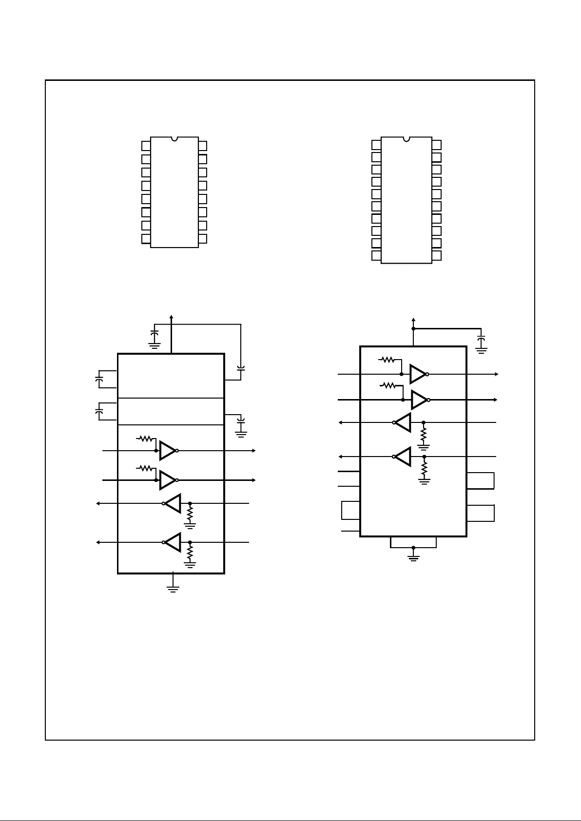
HIN232 (PDIP, CERDIP, SOIC)
TOP VIEW
HIN233 (PDIP, SOIC)
TOP VIEW
Pinouts
(Continued)
14
15
16
9
13
12
11
10
1
2
3
4
5
7
6
8
C1+
V+
C1-
C2+
C2-
R2
IN
T2
OUT
V
CC
T1
OUT
R1
IN
R1
OUT
T1
IN
T2
IN
R2
OUT
GND
V-
11
12
13
14
15
16
17
18
20
19
10
9
8
7
6
5
4
3
2
1
T2
IN
T1
IN
R1
OUT
R1
IN
T1
OUT
GND
(V+) C1+
V
CC
GND
(V-) C2-
R2
OUT
T2
OUT
VC2-
R2
IN
C2+
V+ (C1-)
C1- (C1+)
V- (C2+)
C2+ (C2-)
NOTE: Pin numbers in parentheses are for SOIC Package.
V
CC
+5V
2
V+
16
T1
OUT
T2
OUT
T1
IN
T2
IN
T1
T2
11
10
14
7
+5V
400kΩ
+5V
400kΩ
R1
OUT
R1
IN
R1
1312
5kΩ
R2
OUT
R2
IN
R2
89
5kΩ
+10V TO -10V
VOLTAGE INVERTER
1µF
6
V-
C2+
C2-
+
1µF
4
5
+5V TO 10V
VOLTAGE INVERTER
C1+
C1-
+
1µF
1
3
+
1µF
+
+
1µF
15
6
V
CC
T1
OUT
T2
OUT
R1
OUT
R2
IN
T1
IN
T2
IN
R1
IN
T1
+5V
+
0.1µF
4
5
1
2
18
14 (8)
19
8 (13)
12 (10)
V+
V-
C1+
C1-
C2+
C2-
+5V
400kΩ
GND
9
GND
17
R2
OUT
NO
CONNECT
INTERNAL
-10V
SUPPLY
INTERNAL
+10V
SUPPLY
V-
C2+
C2-
13 (14)
5kΩ
6
20
11 (12)
15
16
10 (11)
3
T2
+5V
400kΩ
5kΩ
HIN230 thru HIN241
 Loading...