

SEMICONDUCTOR
August 1996
CDP6402,
CDP6402C
CMOS Universal Asynchronous
Receiver/Transmitter (UART)
Features
• Low Power CMOS Circuitry. . . . . . . . . . 7.5mW (Typ) at
3.2MHz (Max Freq.) at V
DD
= 5V
• Baud Rate
- DC to 200K Bits/s (Max) at. . . . . . . . . . . . . . 5V, 85oC
- DC to 400K Bits/s (Max) at. . . . . . . . . . . . . .10V, 85
o
• 4V to 10.5 Operation
• Automatic Data Formatting and Status Generation
• Fully Programmable with Externally Selectable Word
Length (5 - 8 Bits), Parity Inhibit, Even/Odd Parity, and
1, 1-1/2, or 2 Stop Bits
• Operating Temperature Range
- CDP6402D, CD . . . . . . . . . . . . . . . . . -55
- CDP6402E, CE . . . . . . . . . . . . . . . . . . -40
o
C to +125oC
o
C to +85oC
• Replaces Industry Type IM6402 and Compatible with
HD6402
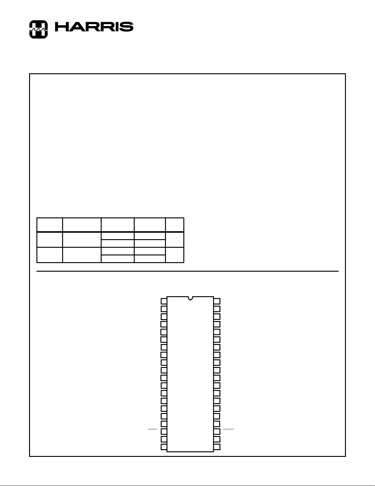
Ordering Information
PACK-
AGE TEMP. RANGE
PDIP -40oC to +85oC CDP6402CE CDP6402E
Burn-In CDP6402CEX -
SBDIP -40
Burn-In CDP6402CDX CDP6402DX
o
C to +85oC CDP6402CD CDP6402D
5V/200K
BAUD
10V/400K
BAUD
PKG.
NO.
E40.6
D40.6
Description
The CDP6402 and CDP6402C are silicon gate CMOS
Universal Asynchronous Receiver/Transmitter (UART)
circuits for interfacing computers or microprocessors to
asynchronous serial data channels. They are designed to
provide the necessary formatting and control for interfacing
C
between serial and parallel data channels. The receiver
converts serial start, data, parity, and stop bits to parallel
data verifying proper code transmission, parity and stop bits.
The transmitter converts parallel data into serial form and
automatically adds start parity and stop bits.
The data word can be 5, 6, 7 or 8 bits in length. Parity may
be odd, even or inhibited. Stop bits can be 1, 1-1/2, or 2
(when transmitting 5-bit code).
The CDP6402 and CDP6402C can be used in a wide range
of applications including modems, printers, peripherals,
video terminals, remote data acquisition systems, and serial
data links for distributed processing systems.
The CDP6402 and CDP6402C are functionally identical.
They differ in that the CDP6402 has a recommended
operating voltage range of 4V to 10.5V, and the CDP6402C
has a recommended operating voltage range of 4V to 6.5V.
Pinout
(40 LEAD PDIP, SBDIP)
TOP VIEW
V
1
DD
2
NC
3
GND
4
RRD
5
RBR8
6
RBR7
7
RBR6
8
RBR5
9
RBR4
10
RBR3
11
RBR2
12
RBR1
PE
13
FE
14
OE
15
SFD
16
RRC
17
18
DRR
19
DR
20
RRI
TRC
40
EPE
39
CLS1
38
CLS2
37
SBS
36
PI
35
CRL
34
TBR8
33
TBR7
32
TBR6
31
TBR5
30
TBR4
29
TBR3
28
TBR2
27
TBR1
26
TRO
25
TRE
24
23
TBRL
22
TBRE
21
MR
CAUTION: These devices are sensitive to electrostatic discharge. Users should follow proper IC Handling Procedures.
Copyright
© Harris Corporation 1996
5-74
File Number 1328.2
CDP6402, CDP6402C
TBR1 (LSB)TBR8 (MSB)
TRE
TBRL
TRC
CLS1
CLS2
CRL
MR
RRC
DRR
SFD
TRANSMITTER
TIMING
AND
CONTROL
RECEIVER
TIMING
AND
CONTROL
STOP
LOGIC
PARITY
LOGIC
PARITY
LOGIC
CONTROL
REGISTER
THREE
STATE
BUFFERS
TRANSMITTER BUFFER REGISTER
TRANSMITTER REGISTER
MULTIPLEXER
MULTIPLEXER
RECEIVER REGISTER
RECEIVER BUFFER REGISTER
STARTSTOP
TRO
SBS
EPE
PI
RRI
START
LOGIC
RRD
RBR1 (LSB)RBR8 (MSB)PEFETBREOEDR
FIGURE 1. FUNCTIONAL BLOCK DIAGRAM
5-75
CDP6402, CDP6402C
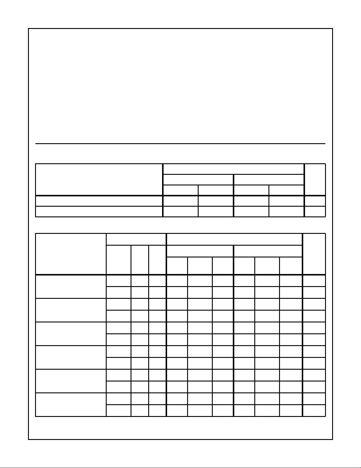
Absolute Maximum Ratings Thermal Information
DC Supply-Voltage Range, (VDD)
CDP6402 . . . . . . . . . . . . . . . . . . . . . . . . . . . . . . . . . .-0.5 to +11V
CDP6402C . . . . . . . . . . . . . . . . . . . . . . . . . . . . . . . . . .-0.5 to +7V
Input Voltage Range, All Inputs . . . . . . . . . . . . . . -0.5 to VDD +0.5V
DC Input Current, Any One Input. . . . . . . . . . . . . . . . . . . . . . . . ±100µA
Device Dissipation Per Output Transistor
For TA = Full Package-Temperature Range
(All Package Types) . . . . . . . . . . . . . . . . . . . . . . . . . . . . . 100mW
Operating-Temperature Range (TA)
Package Type D (SBDIP) . . . . . . . . . . . . . . . . . . -55oC to +125oC
Package Type E (PDIP) . . . . . . . . . . . . . . . . . . . . -40oC to +85oC
CAUTION: Stresses above those listed in “Absolute Maxim um Ratings” ma y cause permanent damage to the device . This is a stress only rating and oper ation of
the device at these or any other conditions above those indicated in the operational sections of this specification is not implied.
NOTE:
1. θJA is measured with the component mounted on an evaluation PC board in free air.
Thermal Resistance (Typical, Note 1) θJA (oC/W) θJC (oC/W)
PDIP Package. . . . . . . . . . . . . . . . . . . 50 N/A
SBDIP Package. . . . . . . . . . . . . . . . . . 55 15
Maximum Storage Temperature Range (T
) . . .-65oC to +150oC
STG
Maximum Lead Temperature (Soldering 10s):
At Distance 1/16 ±1/32 inch (1.59 ±0.79mm) . . . . . . . . . . +265oC
Operating Conditions At T
= Full Package-Temperature Range. For maximum reliability, operating conditions should be selected so
A
that operatIon is always within the following ranges:
LIMITS
CDP6402 CDP6402C
PARAMETER
MIN MAX MIN MAX
DC Operating Voltage Range 4 10.5 4 6.5 V
Input Voltage Range V
Static Electrical Specifications at T
= -40oC to +85oC, VDD±10%, Except as noted
A
SS
V
DD
V
SS
V
DD
CONDITIONS LIMITS
CDP6402 CDP6402C
PARAMETER
Quiescent Device
I
DD
V
O
(V)
- 0, 5 5 - 0.01 50 - 0.02 200 µA
V
(V)
V
IN
DD
(V)
MIN
(NOTE 1)
TYP MAX MIN
(NOTE 1)
TYP MAX
Current
- 0,10 10 - 1 200 - - - µA
Output Low Drive
I
OL
0.4 0,5 5 2 4 - 1.2 2.4 - mA
(Sink) Current
0.5 0,10 10 5 7 - - - - mA
UNITS
V
UNITS
Output High Drive
(Source) Current
Output Voltage LowLevel (Note 2)
Output Voltage
High Level (Note 2)
Input Low Voltage V
I
OH
4.6 0, 5 5 -0.55 -1.1 - -0.55 -1.1 - mA
9.5 0,10 10 -1.3 -2.6 - - - - mA
V
OL
- 0, 5 5 - 0 0.1 - 0 0.1 V
- 0, 10 10 - 0 0.1 - - - V
V
OH
- 0, 5 5 4.9 5 - 4.9 5 - V
- 0, 10 10 9.9 10 - - - - V
0.5, 4.5 - 5 - - 0.8 - - 0.8 V
IL
0.5, 9.5 - 10 - - 0.2 V
DD
---V
5-76
CDP6402, CDP6402C
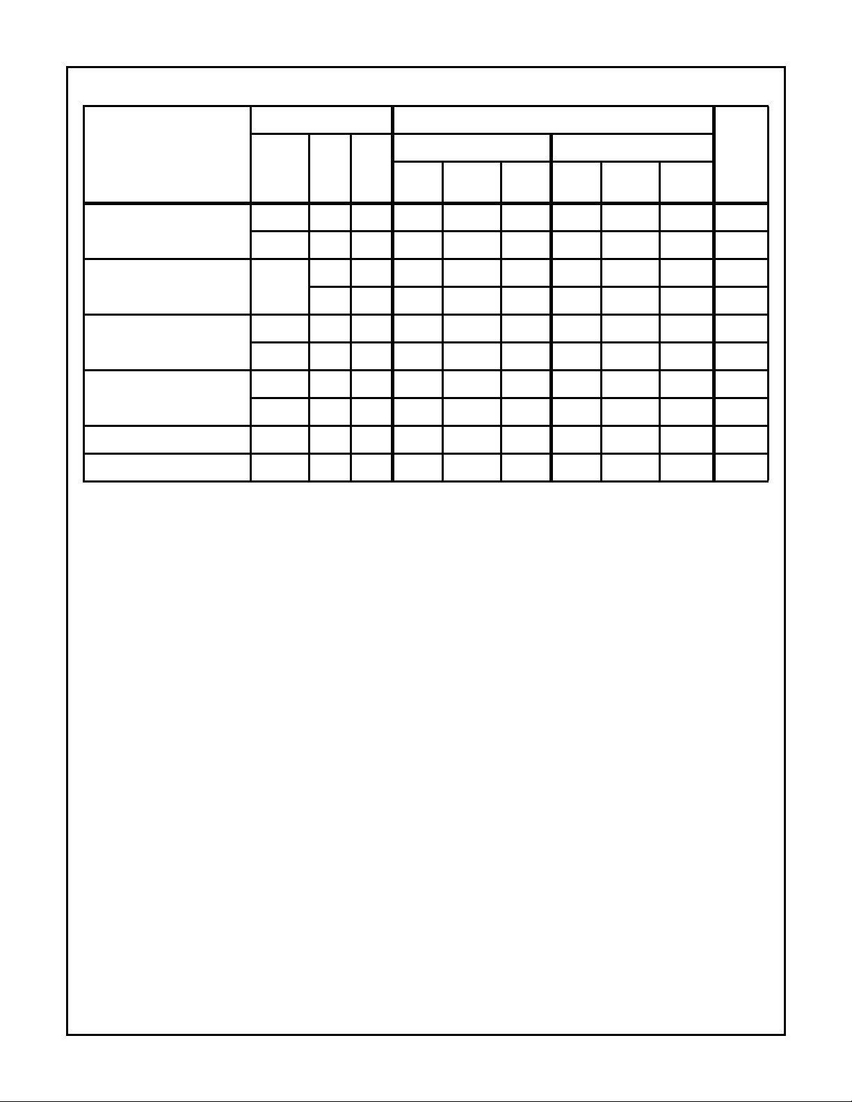
Static Electrical Specifications at T
CONDITIONS LIMITS
V
O
PARAMETER
Input High Voltage V
Input Leakage
Current
Three-State Output
Leakage Current
Operating Current
(Note 2)
Input Capacitance C
Output Capacitance C
I
I
OUT
I
DD1
OUT
IH
IN
IN
(V)
0.5, 4.5 - 5 VDD-2 - - VDD-2 - - V
0.5, 9.5 - 10 7 - - - - - V
Any
Input
0, 5 0, 5 5 - ±10
0, 10 0,10 10 - ±10
- 0, 5 5 - 1.5 − - 1.5 - mA
- 0,10 10 - 10 − -- -mA
- - - - 5 7.5 - 5 7.5 pF
- - - - 10 15 - 10 15 pF
= -40oC to +85oC, VDD±10%, Except as noted (Continued)
A
CDP6402 CDP6402C
V
V
IN
(V)
DD
(V)
0,5 5 - ±10
0,10 10 - ±10
MIN
(NOTE 1)
TYP MAX MIN
-4
-4
-4
-4
±1- - ±1µA
±2- - - µA
±1-±10
±10 - - - µA
(NOTE 1)
TYP MAX
-4
UNITS
±1 µA
NOTES:
1. Typical values are for TA= 25oC and nominal V
DD
2. IOL = IOH = 1µA.
3. Operating current is measured at 200kHz or VDD = 5V and 400kHz for VDD = 10V, with open outputs (worst-case frequencies for
CDP1802A system operating at maximum speed of 3.2MHz).
5-77

Description of Operation
CDP6402, CDP6402C
Initialization and Controls
A positive pulse on the MASTER RESET (MR) input resets
the control, status, and receiver buffer registers, and sets the
serial output (TRO) High. Timing is generated from the clock
inputs RRC and TRC at a frequency equal to 16 times the
serial data bit rate. The RRC and TRC inputs may be driven
by a common clock, or may be driven independently by two
different clocks. The CONTROL REGISTER LOAD (CRL)
input is strobed to load control bits for PARITY INHIBIT (PI),
EVEN PARITY ENABLE (EPE), STOP BIT SELECTS (SBS),
and CHARACTER LENGTH SELECTS (CLS1 and CLS2).
These inputs may be hand wired to V
V
. When the initialization is completed, the UART is ready
DD
or VDD with CRL to
SS
for receiver and/or transmitter operations.
Transmitter Operation
The transmitter section accepts parallel data, formats it, and
transmits it in serial form (Figure 2) on the TRO terminal.
1, 1-1/2 OR
MSB
2 STOP BITS
†
P ARITY
START
BIT
† IF ENABLED
5 - 8 DATA BITS
LSB
FIGURE 2. SERIAL DATA FORMAT
Transmitter timing is shown in Figure 3. (A) Data is loaded
into the transmitter buffer register from the inputs TBR1
through TBR8 by a logic low on the
must be present at least t
rising edge of
TBRL. If words less than 8-bits are used, only
prior to, and tTD following, the
DT
TBRL input. Valid data
the least significant bits are used. The character is right justified into the least significant bit, TBR1. (B) The rising edge of
TBRL clears TBRE. 1/2 to 11/2 cycles later, depending on
when the
TBRL pulse occurs with respect to TRC, data is
transferred to the transmitter register and TRE is cleared.
TBRE is set to a logic High one cycle after that.
Output data is clocked by TRC. The clock rate is 16 times
the data rate. (C) A second pulse on
TBRL loads data into
the transmitter buffer register. Data transfer to the transmitter
register is delayed until transmission of the current character
is complete. (D) Data is automatically transferred to the
transmitter register and transmission of that character
begins.
TBRL
TBRE
TRE
TRO DATA
A
FIGURE 3. TRANSMITTER TIMING WAVEFORMS
1-1/2 TO 2-1/2 CYCLES
1/2 TO 1-1/2 CYCLES
1 TO 2 CYCLES
BC D
1/2
CLOCK
END OF
LAST
STOP BIT
Receiver Operation
Data is received in serial form at the RRl input. When no
data is being received, RRI input must remain high. The data
is clocked through the RRC. The clock rate is 16 times the
data rate. Receiver timing is shown in Figure 4.
BEGINNING OF FIRST STOP BIT
RRI
RBRI-8, OE
DRR
DR
FE, PE
ABC
FIGURE 4. RECEIVER TIMING WAVEFORMS
(A) A low level on
DRR clears the DR line. (B) During the first
8 1/2 TO 9 1/2
CLOCK CYCLES
1/2 CLOCK
CYCLES
stop bit data is transferred from the receiver register to the
RB Register. If the word is less than 8 bits, the unused most
significant bits will be a logic low. The output character is
right justified to the least significant bit RBR1. A logic high on
OE indicates overruns. An overrun occurs when DR has not
been cleared before the present character was transf erred to
the RBR. (C) 1/2 clock cycle later DR is set to a logic high
and FE is evaluated. A logic high on FE indicates an invalid
stop bit was received. A logic high on PE indicates a parity
error.
Start Bit Detection
The receiver uses a 16X clock for timing (Figure 5). The start
bit could have occurred as much as one clock cycle before it
was detected, as indicated by the shaded portion. The center of the start bit is defined as clock count 7 1/2. If the
receiver clock is a symmetrical square wave, the center of
the start bit will be located within ±1/2 clock cycle ±1/32 bit or
±3.125%. The receiver begins searching for the next start bit
at 9 clocks into the first stop bit.
COUNT 7 1/2
DEFINED CENTER
OF STAR T BIT
CLOCK
RRI
INPUT
ASTART
7 1/2 CLOCK
CYCLES
8 1/2 CLOCK
CYCLES
FIGURE 5. START BIT TIMING WAVEFORMS
5-78

CDP6402, CDP6402C
TABLE 1. CONTROL WORD FUNCTION
CONTROL WORD
DATA BITS PARITY BIT STOP BIT (S)CLS2 CLS1 PI EPE SBS
LLLLL5 ODD1
LLLLH5 ODD1.5
L L L H L 5 EVEN 1
L L L H H 5 EVEN 1.5
L L H X L 5 DISABLED 1
L L H X H 5 DISABLED 1.5
LHLLL6 ODD1
L H L L H 6 ODD 2
L H L H L 6 EVEN 1
L H L H H 6 EVEN 2
L H H X L 6 DISABLED 1
L H H X H 6 DISABLED 2
HLLLL7 ODD1
H L L L H 7 ODD 2
H L L H L 7 EVEN 1
H L L H H 7 EVEN 2
H L H X L 7 DISABLED 1
H L H X H 7 DISABLED 2
HHLLL8 ODD1
H H L L H 8 ODD 2
H H L H L 8 EVEN 1
H H L H H 8 EVEN 2
H H H X L 8 DISABLED 1
H H H X H 8 DISABLED 2
NOTE: X = Don’t Care
5-79

CDP6402, CDP6402C
TABLE 2. FUNCTION PIN DEFINITION
PIN SYMBOL DESCRIPTION
1VDDPositive Power Supply
2 N/C No Connection
3 GND Ground (VSS)
4 RRD A high level on RECEIVER REGISTER DISABLE forces the receiver holding register ouputs RBR1-RBR8 to
a high impedance state.
5 RBR8 The contents of the RECEIVER BUFFER REGISTER appear on these three-state outputs. Word formats less
than 8 characters are right justified to RBR1.
6 RBR7
7 RBR6
8 RBR5
9 RBR4
10 RBR3
11 RBR2
12 RBR1
13 PE A high level on PARITY ERROR indicates that the received parity does not match parity programmed by control
14 FE A high level on FRAMING ERROR indicates the first stop bit was invalid. FE will sta y active until the next valid
15 OE A high level on OVERRUN ERROR indicates the data received flag was not cleared before the last character
16 SFD A high level on STATUS FLAGS DISABLE forces the outputs PE, FE, OE, DR, TBRE to a high impedance
17 RRC The RECEIVER REGISTER CLOCK is 16X the receiver data rate.
18 DRR A low level on DATA RECEIVED RESET clears the data received output (DR), to a low level.
19 DR A high lev el on DAT A RECEIVED indicates a char acter has been received and transf erred to the receiver b uffer
20 RRl Serial data on RECEIVER REGISTER INPUT is clocked into the receiver register.
See Pin 5 - RBR8
bits. The output is active until parity matches on a succeeding character. When parity is inhibited, this output
is low.
character’s stop bit is received.
was transferred to the receiver b uffer register . The Error is reset at the next char acter’s stop bit if DRR has been
performed (i.e., DRR; active low).
state.
register.
21 MR A high level on MASTER RESET (MR) clears PE, FE, OE and DR, and sets TRE, TBRE, and TRO. TRE is
actually set on the first rising edge of TRC after MR goes high. MR should be strobed after power-up.
22 TBRE A high level on TRANSMITTER BUFFER REGISTER EMPTY indicates the transmitter buffer register has
transferred its data to the transmitter register and is ready for new data.
23 TBRL A low level on TRANSMITTER BUFFER REGISTER LOAD transfers data from inputs TBR1-TBR8 into the
transmitter buffer register. A low to high transition on TBRL requests data transfer to the transmitter register. If
the transmitter register is busy, transfer is automatically delayed so that the two characters are transmitted end
to end.
24 TRE A high level on TRANSMITTER REGISTER EMPTY indicates completed transmission of a char acter including
stop bits.
5-80

CDP6402, CDP6402C
TABLE 2. FUNCTION PIN DEFINITION (Continued)
PIN SYMBOL DESCRIPTION
25 TRO Character data, start data and stop bits appear serially at the TRANSMITTER REGISTER OUTPUT.
26 TBR1 Character data is loaded into the TRANSMITTER BUFFER REGISTER via inputs TBR1-TBR8. For character
formats less than 8 bits, the TBR8, 7, and 6 Inputs are ignored corresponding to the programmed word length.
27 TBR2
28 TBR3
29 TBR4
30 TBR5
31 TBR6
32 TBR7
33 TBR8
34 CRL A high level on CONTROL REGISTER LOAD loads the control register.
35 PI† A high level on PARITY INHIBIT inhibits parity generation, parity checking and forces PE output low.
36 SBS† A high level on STOP BIT SELECT selects 1.5 stop bits for a 5 character format and 2 stop bits for other
37 CLS2† These inputs program the CHARACTER LENGTH SELECTED. (CLS1 low CLS2 low 5 bits) (CLS1 high CLS2
38 CLSl† See Pin 37 - CLS2
39 EPE† When PI is low, a high level on EVEN PARITY ENABLE generates and checks even parity . A lo w level selects
40 TRC The TRANSMITTER REGISTER CLOCK is 16X the transmit data rate.
† See Table 1 (Control Word Function)
See Pin 26 - TBR1
lengths.
low 6 bits) (CLS1 low CLS2 high 7 bits) (CLS1 high CLS2 high 8 bits).
odd parity.
5-81

CDP6402, CDP6402C
Dynamic Electrical Specifications at T
= -40oC to +85oC, VDD±5%, tR, tF = 20ns, VIH = 0.7 VDD, VIL = 0.3 VDD, CL = 100pF
A
LIMITS
CDP6402 CDP6402C
(NOTE 1)
PARAMETER
V
(V)
DD
(NOTE 2)
TYP
(NOTE 3)
MAX
SYSTEM TIMING (See Figure 6)
Minimum Pulse Width
CRL
Minimum Setup Time
Control Word to CRL
Minimum Hold Time
Control Word after CRL
Propagation Delay Time
SFD High to SOD
SFD Low to SOD t
t
CRL
t
CWC
t
CCW
t
SFDH
SFDL
5 50 150 50 150 ns
10 40 100 - - ns
5 20502050ns
10 0 40 - - ns
5 40604060ns
10 20 30 - - ns
5 130 200 130 200 ns
10 100 150 - - ns
5 130 200 130 200 ns
10 40 60 - - ns
RRD High to Receiver Register
High Impedance
RRD Low to Receiver Register
Active
Minimum Pulse Width
MR
t
RRDH
t
RRDL
5 80 150 80 150 ns
10 40 70 - - ns
5 80 150 80 150 ns
10 40 70 - - ns
5 200 400 200 400 ns
10 100 200 - - ns
NOTES:
1. All measurements are made at the 50% point of the transition except three-state measurements.
2. Typical values for TA = 25oC and nominal VDD.
3. Maximum limits of minimum characteristics are the values above which all devices function.
(NOTE 2)
TYP
(NOTE 3)
MAX
UNITS
CONTROL WORD INPUT
CRL
STATUS OUTPUTS
SFD
R BUS 0
R BUS 7
RRD
CONTROL INPUT WORD TIMING
CONTROL WORD BYTE
t
CWC
t
CRL
STATUS OUTPUT TIMING
t
SFDH
RECEIVER REGISTER DISCONNECT TIMING
t
RRDH
90%
10%
90%
10%
FIGURE 6. SYSTEM TIMING WAVEFORMS
5-82
70%
30%
70%
30%
t
CCW
t
RRDL
t
SFDL

CDP6402, CDP6402C
Dynamic Electrical Specifications at T
(NOTE 1)
PARAMETER
TRANSMITTER TIMING (See Figure 7)
Minimum Clock Period (TRC) t
Minimum Pulse Width
Clock Low Level t
Clock High Level t
TBRL t
Minimum Setup Time
TBRL to Clock t
= -40oC to +85oC, VDD±5%, tR, tF = 20ns, VIH = 0.7 VDD, VIL = 0.3 VDD, CL = 100pF
A
LIMITS
CDP6402 CDP6402C
CC
V
DD
(V)
(NOTE 2)
TYP
5 250 310 250 310 ns
(NOTE 3)
MAX
(NOTE 2)
TYP
(NOTE 3)
MAX
UNITS
10 125 155 - - ns
CL
5 100 125 100 125 ns
10 75 100 - - ns
CH
5 100 125 100 125 ns
10 75 100 - - ns
THTH
5 80 200 80 200 ns
10 40 100 - - ns
THC
5 175 275 175 275 ns
10 90 150 - - ns
Data to TBRL t
DT
5 20502050ns
10 0 40 - - ns
Minimum Hold-Time
Data after TBRL t
TD
5 40604060ns
10 20 30 - - ns
Propagation Delay Time
Clock to Data Start Bit t
CD
5 300 450 300 450 ns
10 150 225 - - ns
Clock to TBRE t
CT
5 330 400 330 400 ns
10 100 150 - - ns
TBRL to TBRE t
TTHR
5 200 300 200 300 ns
10 100 150 - - ns
Clock to TRE t
TTS
5 330 400 330 400 ns
10 100 150 - - ns
NOTES:
1. All measurements are made at the 50% point of the transition except three-state measurements.
2. Typical values for TA = 25oC and nominal VDD.
3. Maximum limits of minimum characteristics are the values above which all devices function.
5-83

CDP6402, CDP6402C
TRANSMITTER BUFFER
REGISTER LOADED
(NOTE 1)
t
CC
t
THC
t
t
THTH
TTHR
t
DT
t
CL
DAT A
TRC
TBRL
TRO
TBRE
TRE
T BUS 0
T BUS 7
t
CH
NOTES:
1. The holding register is loaded on the trailing edge of TBRL.
2. The transmitter shift register, if empty , is loaded on the first high-to-low transition of the clock which occurs at least 1/2 clock period +
t
after the trailing edge of TBRL and transmission of a start bit occurs 1/2 clock period + tCD later.
THC
FIGURE 7. TRANSMITTER TIMING WAVEFORMS
TRANSMITTER SHIFT
REGISTER LOADED
(NOTE 2)
12
t
TTS
t
DT
34567141516123
t
CD
1ST DATA BIT
t
CT
t
CD
RRC
(NOTE 1)
RRI
R BUS 0 -
R BUS 7
DR
DRR
OE
(NOTE 2)
PE
FE
t
CC
t
CH
t
CL
12
t
DC
CLOCK 7 1/2
SAMPLE
3456716
START BIT PARITY
t
DDA
t
DD
123456789
STOP BIT 1
CLOCK 7 1/2 LOAD
HOLDING REGISTER
t
COE
t
CPE
t
CFE
t
CDV
DAT A
t
CDA
NOTES:
1. If a start bit occurs at a time less than tDC before a high-to-low transition of the clock, the start bit may not be recognized until the next
high-to-low transition of the clock. The start bit may be completely asynchronous with the clock.
2. If a pending DA has not been cleared by a read of the receiver holding register by the time a new word is loaded into the receiver holding
register, the OE signal will come true..
FIGURE 8. RECEIVER TIMING WAVEFORMS
5-84

CDP6402, CDP6402C
Dynamic Electrical Specifications at T
(NOTE 1)
PARAMETERS
RECEIVER TIMING (See Figure 8)
Minimum Clock Period (RRC) t
Minimum Pulse Width
Clock Low Level t
Clock High Level t
Data Received Reset t
Minimum Setup Time
Data Start Bit to Clock t
= -40oC to +85oC, VDD±5%, tR, tF = 20ns, VIH = 0.7 VDD, VIL = 0.3 VDD, CL = 100pF
A
LIMITS
CDP6402 CDP6402C
CC
V
DD
(V)
(NOTE 2)
TYP
5 250 310 250 310 ns
(NOTE 3)
MAX
(NOTE 2)
TYP
(NOTE 3)
MAX
UNITS
10 125 155 - - ns
CL
5 100 125 100 125 ns
10 75 100 - - ns
CH
5 100 125 100 125 ns
10 75 100 - - ns
DD
5 50755075ns
10 25 40 - - ns
DC
5 100 150 100 150 ns
10 50 75 - - ns
Propagation Delay Time
Data Received Reset to
t
DDA
5 150 250 150 250 ns
Data Received
10 75 125 - - ns
Clock to Data Valid t
CDV
5 275 400 275 400 ns
10 110 175 - - ns
Clock to DR t
CDA
5 275 400 275 400 ns
10 110 175 - - ns
Clock to Overrun Error t
COE
5 275 400 275 400 ns
10 100 150 - - ns
Clock to Parity Error t
CPE
5 240 375 240 375 ns
10 120 17 - - ns
Clock to Framing Error t
CFE
5 200 300 200 300 ns
10 100 150 - - ns
NOTES:
1. All measurements are made at the 50% point of the transition except three-state measurements.
2. Typical values for TA = 25oC and nominal VDD.
3. Maximum limits of minimum characteristics are the values above which all devices function.
5-85
 Loading...