SEMICONDUCTOR
August 1996
CDP6402,
CDP6402C
CMOS Universal Asynchronous
Receiver/Transmitter (UART)
Features
• Low Power CMOS Circuitry. . . . . . . . . . 7.5mW (Typ) at
3.2MHz (Max Freq.) at V
DD
= 5V
• Baud Rate
- DC to 200K Bits/s (Max) at. . . . . . . . . . . . . . 5V, 85oC
- DC to 400K Bits/s (Max) at. . . . . . . . . . . . . .10V, 85
o
• 4V to 10.5 Operation
• Automatic Data Formatting and Status Generation
• Fully Programmable with Externally Selectable Word
Length (5 - 8 Bits), Parity Inhibit, Even/Odd Parity, and
1, 1-1/2, or 2 Stop Bits
• Operating Temperature Range
- CDP6402D, CD . . . . . . . . . . . . . . . . . -55
- CDP6402E, CE . . . . . . . . . . . . . . . . . . -40
o
C to +125oC
o
C to +85oC
• Replaces Industry Type IM6402 and Compatible with
HD6402
Ordering Information
PACK-
AGE TEMP. RANGE
PDIP -40oC to +85oC CDP6402CE CDP6402E
Burn-In CDP6402CEX -
SBDIP -40
Burn-In CDP6402CDX CDP6402DX
o
C to +85oC CDP6402CD CDP6402D
5V/200K
BAUD
10V/400K
BAUD
PKG.
NO.
E40.6
D40.6
Description
The CDP6402 and CDP6402C are silicon gate CMOS
Universal Asynchronous Receiver/Transmitter (UART)
circuits for interfacing computers or microprocessors to
asynchronous serial data channels. They are designed to
provide the necessary formatting and control for interfacing
C
between serial and parallel data channels. The receiver
converts serial start, data, parity, and stop bits to parallel
data verifying proper code transmission, parity and stop bits.
The transmitter converts parallel data into serial form and
automatically adds start parity and stop bits.
The data word can be 5, 6, 7 or 8 bits in length. Parity may
be odd, even or inhibited. Stop bits can be 1, 1-1/2, or 2
(when transmitting 5-bit code).
The CDP6402 and CDP6402C can be used in a wide range
of applications including modems, printers, peripherals,
video terminals, remote data acquisition systems, and serial
data links for distributed processing systems.
The CDP6402 and CDP6402C are functionally identical.
They differ in that the CDP6402 has a recommended
operating voltage range of 4V to 10.5V, and the CDP6402C
has a recommended operating voltage range of 4V to 6.5V.
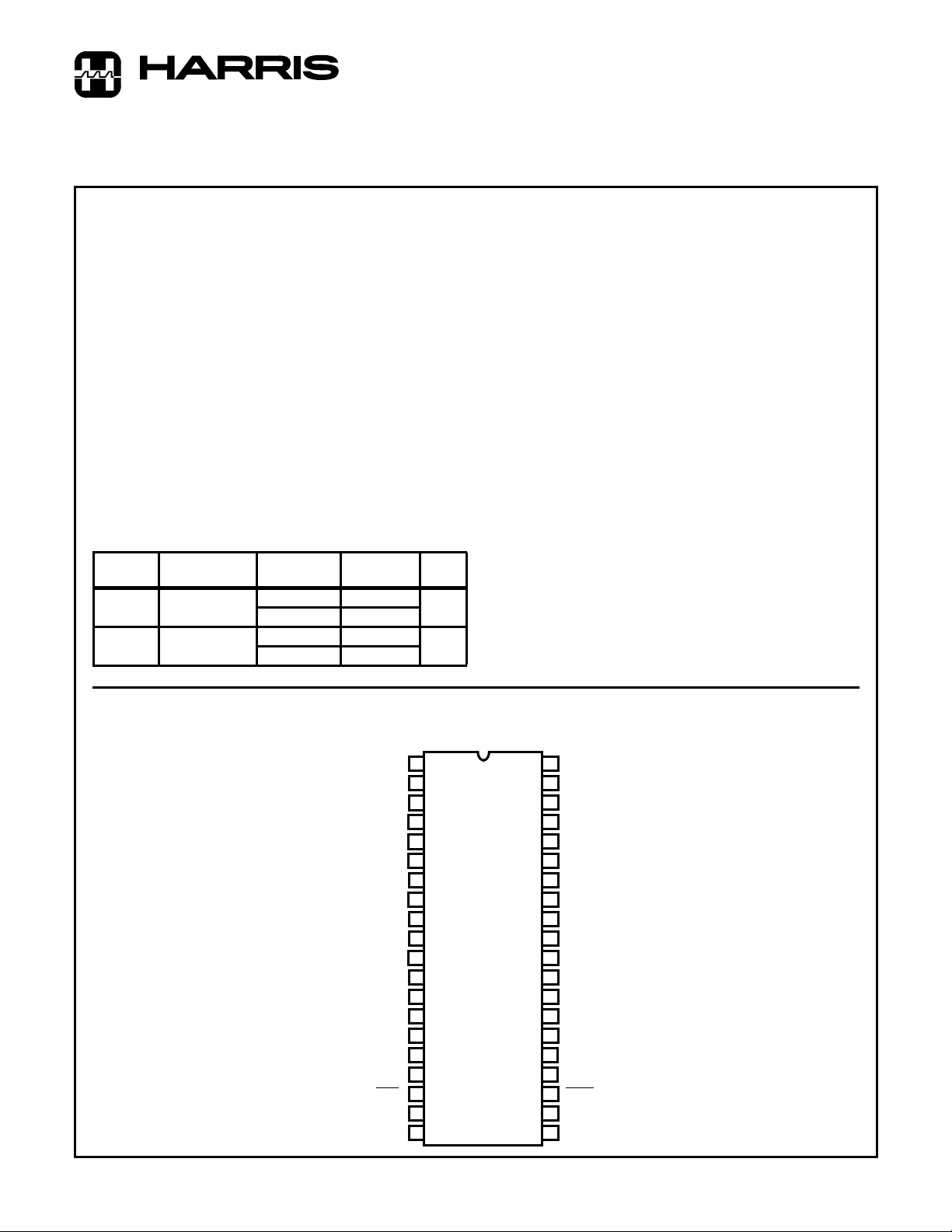
Pinout
(40 LEAD PDIP, SBDIP)
TOP VIEW
V
1
DD
2
NC
3
GND
4
RRD
5
RBR8
6
RBR7
7
RBR6
8
RBR5
9
RBR4
10
RBR3
11
RBR2
12
RBR1
PE
13
FE
14
OE
15
SFD
16
RRC
17
18
DRR
19
DR
20
RRI
TRC
40
EPE
39
CLS1
38
CLS2
37
SBS
36
PI
35
CRL
34
TBR8
33
TBR7
32
TBR6
31
TBR5
30
TBR4
29
TBR3
28
TBR2
27
TBR1
26
TRO
25
TRE
24
23
TBRL
22
TBRE
21
MR
CAUTION: These devices are sensitive to electrostatic discharge. Users should follow proper IC Handling Procedures.
Copyright
© Harris Corporation 1996
5-74
File Number 1328.2

CDP6402, CDP6402C
TBR1 (LSB)TBR8 (MSB)
TRE
TBRL
TRC
CLS1
CLS2
CRL
MR
RRC
DRR
SFD
TRANSMITTER
TIMING
AND
CONTROL
RECEIVER
TIMING
AND
CONTROL
STOP
LOGIC
PARITY
LOGIC
PARITY
LOGIC
CONTROL
REGISTER
THREE
STATE
BUFFERS
TRANSMITTER BUFFER REGISTER
TRANSMITTER REGISTER
MULTIPLEXER
MULTIPLEXER
RECEIVER REGISTER
RECEIVER BUFFER REGISTER
STARTSTOP
TRO
SBS
EPE
PI
RRI
START
LOGIC
RRD
RBR1 (LSB)RBR8 (MSB)PEFETBREOEDR
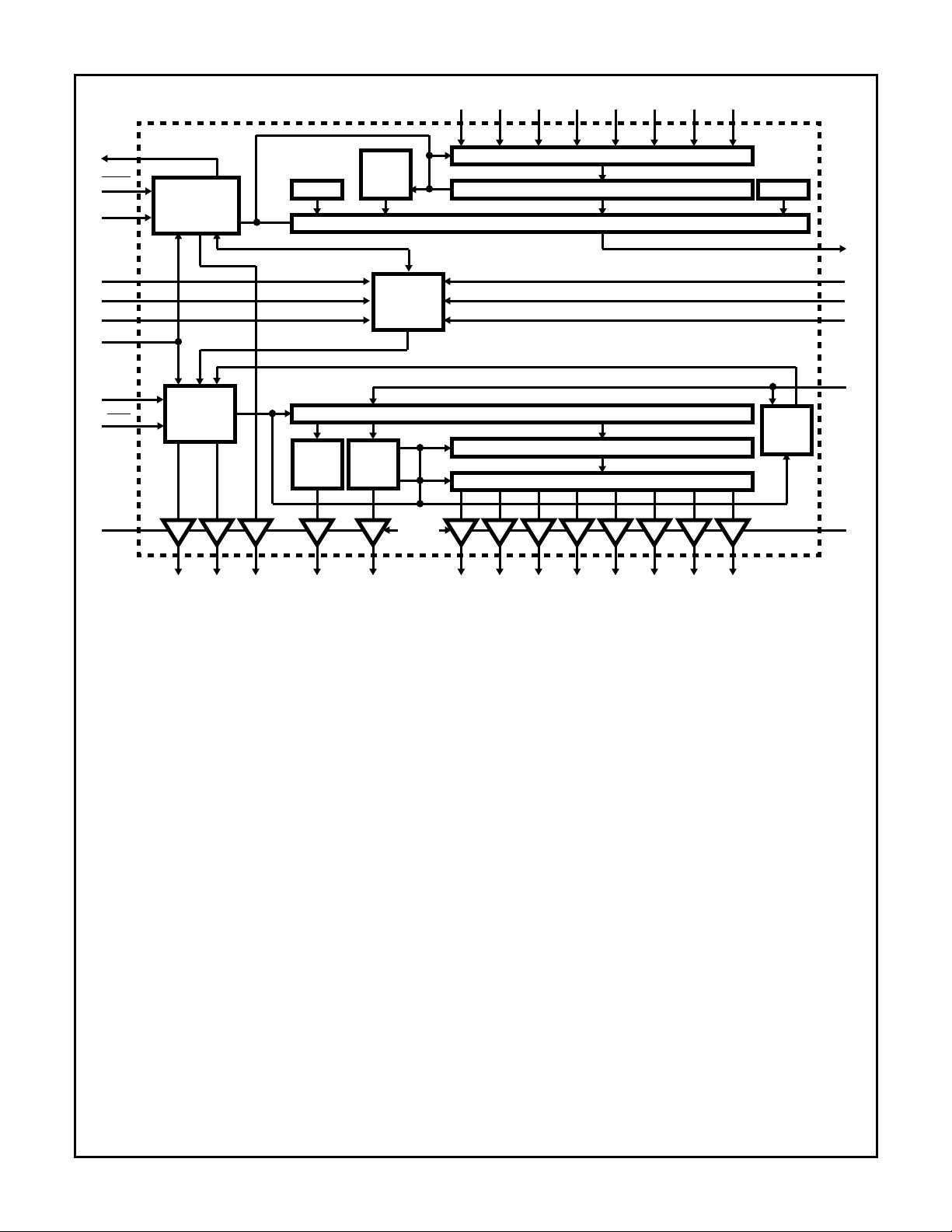
FIGURE 1. FUNCTIONAL BLOCK DIAGRAM
5-75

CDP6402, CDP6402C
Absolute Maximum Ratings Thermal Information
DC Supply-Voltage Range, (VDD)
CDP6402 . . . . . . . . . . . . . . . . . . . . . . . . . . . . . . . . . .-0.5 to +11V
CDP6402C . . . . . . . . . . . . . . . . . . . . . . . . . . . . . . . . . .-0.5 to +7V
Input Voltage Range, All Inputs . . . . . . . . . . . . . . -0.5 to VDD +0.5V
DC Input Current, Any One Input. . . . . . . . . . . . . . . . . . . . . . . . ±100µA
Device Dissipation Per Output Transistor
For TA = Full Package-Temperature Range
(All Package Types) . . . . . . . . . . . . . . . . . . . . . . . . . . . . . 100mW
Operating-Temperature Range (TA)
Package Type D (SBDIP) . . . . . . . . . . . . . . . . . . -55oC to +125oC
Package Type E (PDIP) . . . . . . . . . . . . . . . . . . . . -40oC to +85oC
CAUTION: Stresses above those listed in “Absolute Maxim um Ratings” ma y cause permanent damage to the device . This is a stress only rating and oper ation of
the device at these or any other conditions above those indicated in the operational sections of this specification is not implied.
NOTE:
1. θJA is measured with the component mounted on an evaluation PC board in free air.
Thermal Resistance (Typical, Note 1) θJA (oC/W) θJC (oC/W)
PDIP Package. . . . . . . . . . . . . . . . . . . 50 N/A
SBDIP Package. . . . . . . . . . . . . . . . . . 55 15
Maximum Storage Temperature Range (T
) . . .-65oC to +150oC
STG
Maximum Lead Temperature (Soldering 10s):
At Distance 1/16 ±1/32 inch (1.59 ±0.79mm) . . . . . . . . . . +265oC
Operating Conditions At T
= Full Package-Temperature Range. For maximum reliability, operating conditions should be selected so
A
that operatIon is always within the following ranges:
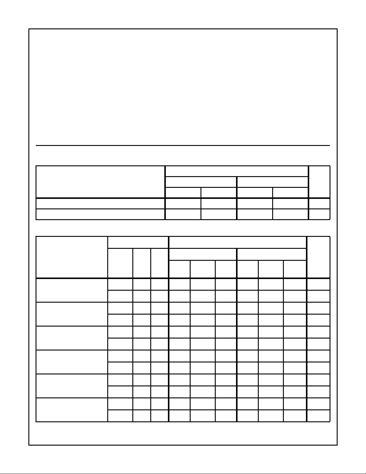
LIMITS
CDP6402 CDP6402C
PARAMETER
MIN MAX MIN MAX
DC Operating Voltage Range 4 10.5 4 6.5 V
Input Voltage Range V
Static Electrical Specifications at T
= -40oC to +85oC, VDD±10%, Except as noted
A
SS
V
DD
V
SS
V
DD
CONDITIONS LIMITS
CDP6402 CDP6402C
PARAMETER
Quiescent Device
I
DD
V
O
(V)
- 0, 5 5 - 0.01 50 - 0.02 200 µA
V
(V)
V
IN
DD
(V)
MIN
(NOTE 1)
TYP MAX MIN
(NOTE 1)
TYP MAX
Current
- 0,10 10 - 1 200 - - - µA
Output Low Drive
I
OL
0.4 0,5 5 2 4 - 1.2 2.4 - mA
(Sink) Current
0.5 0,10 10 5 7 - - - - mA
UNITS
V
UNITS
Output High Drive
(Source) Current
Output Voltage LowLevel (Note 2)
Output Voltage
High Level (Note 2)
Input Low Voltage V
I
OH
4.6 0, 5 5 -0.55 -1.1 - -0.55 -1.1 - mA
9.5 0,10 10 -1.3 -2.6 - - - - mA
V
OL
- 0, 5 5 - 0 0.1 - 0 0.1 V
- 0, 10 10 - 0 0.1 - - - V
V
OH
- 0, 5 5 4.9 5 - 4.9 5 - V
- 0, 10 10 9.9 10 - - - - V
0.5, 4.5 - 5 - - 0.8 - - 0.8 V
IL
0.5, 9.5 - 10 - - 0.2 V
DD
---V
5-76

CDP6402, CDP6402C
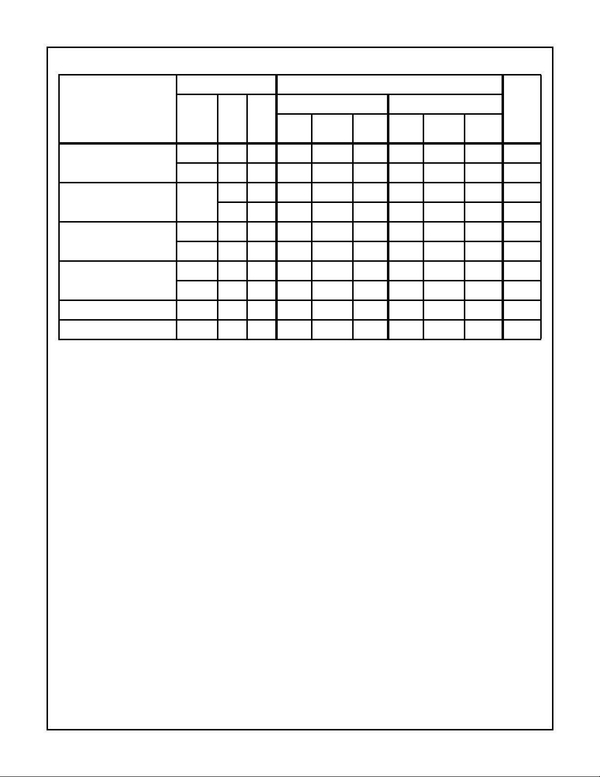
Static Electrical Specifications at T
CONDITIONS LIMITS
V
O
PARAMETER
Input High Voltage V
Input Leakage
Current
Three-State Output
Leakage Current
Operating Current
(Note 2)
Input Capacitance C
Output Capacitance C
I
I
OUT
I
DD1
OUT
IH
IN
IN
(V)
0.5, 4.5 - 5 VDD-2 - - VDD-2 - - V
0.5, 9.5 - 10 7 - - - - - V
Any
Input
0, 5 0, 5 5 - ±10
0, 10 0,10 10 - ±10
- 0, 5 5 - 1.5 − - 1.5 - mA
- 0,10 10 - 10 − -- -mA
- - - - 5 7.5 - 5 7.5 pF
- - - - 10 15 - 10 15 pF
= -40oC to +85oC, VDD±10%, Except as noted (Continued)
A
CDP6402 CDP6402C
V
V
IN
(V)
DD
(V)
0,5 5 - ±10
0,10 10 - ±10
MIN
(NOTE 1)
TYP MAX MIN
-4
-4
-4
-4
±1- - ±1µA
±2- - - µA
±1-±10
±10 - - - µA
(NOTE 1)
TYP MAX
-4
UNITS
±1 µA
NOTES:
1. Typical values are for TA= 25oC and nominal V
DD
2. IOL = IOH = 1µA.
3. Operating current is measured at 200kHz or VDD = 5V and 400kHz for VDD = 10V, with open outputs (worst-case frequencies for
CDP1802A system operating at maximum speed of 3.2MHz).
5-77
 Loading...