Semiconductor
No. AN6157.1 April 1994
APPLICATIONS OF THE CA3085 SERIES MONOLITHIC
IC VOLTAGE REGULATORS
Authors: A.C.N. Sheng and L.R. Avery
The Harris CA3085, CA3085A, and CA3085B monolithic
IC’s are positive-voltage regulators capable of providing output currents up to 100mA over the temperature range from -
o
55
C to +125oC. They are supplied in 8 lead TO-5 type packages. The following tabulation shows some key characteristics and salient differences between devices in the CA3085
Series.
VIN (VI)
RANGE
TYPE
CA3085 7.5 - 30 1.8 - 26 12* 0.1
CA3085A 7.5 - 40 1.7 - 36 100 0.15
CA3085B 7.5 - 50 1.7 - 46 100 0.15
(V)
*This value may be extended to 100mA; however, regulation
is not specified beyond 12mA.
In addition to these differences, the range of some specified
performance parameters is more tightly controlled in the
CA3085B than in the CA3085A, and more in the CA3085A
than in the CA3085.
This note describes the basic circuit of the CA3085 series
devices and some typical applications that include a high
current regulator, constant current regulations, a switching
regulator, a negative-voltage regulator, a dual-tracking regulator, high-voltage regulators, and various methods of providing current limiting, A circuit in which the CA3085 is used as
a general-purpose amplifier is also shown.
Circuit Description
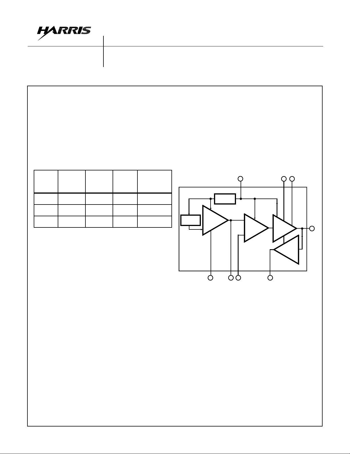
The block diagram of the CA3085 series circuits is shown in
Figure 1. Fundamentally, the circuit consists of a frequency
compensated error-amplifier which compares an internally
generated reference voltage with a sample of the output voltage and controls a series-pass amplifier to regulate the output. The starting circuit assures stable latch-in of the
voltage-reference circuitry. The current-limiting portion of the
circuit is an optional feature that protects the IC in the event
of overload.
Terminal 5 provides a source of stable reference voltage for
auxiliary use; a current of about 250µA can be supplied to an
external circuit without significantly disturbing reference-volt-
V
OUT
RANGE
(V)
(VO)
MAX.
I
OUT
(mA)
(IO)
MAX LOAD
REGULATION
( % VO)
Harris Intelligent Power
age stability. If necessary, filtering of the inherent noise of the
reference-voltage circuit can be accomplished by connecting
a suitable bypass capacitor between terminals 5 and 4.
Terminal 6 (the “inverting input” in accordance with operational-amplifier terminology) is the input through which a
sample of the regulated output voltage is applied.
COMPENSATION AND
UNREGULATED
VOLT.
STARTING
CIRCUIT
SUBSTRATE
REF.
AMPL.
SOURCE
V-
FIGURE 1. BLOCK DIAGRAM OF CA3085 SERIES
INPUT (V
CURRENT
SOURCE
V
REF
+
3
)
IN
+
FREQ.
COMP.
ERROR
AMPL.
-
INV
654 8
INPUT
The collector of the series-pass output transistor is brought
out separately at terminal 2 (“current booster”) to provide
base drive for an external p-n-p transistor; this approach is
one method of regulating currents greater than 100mA.
Because the voltage regulator is essentially an operational
amplifier having considerable feedback, frequency compensation is necessary in some circuits to prevent oscillations.
Terminal 7 is provided for if external frequency compensation is necessary. Terminal 7 can also be used to “inhibit”
(strobe, squelch, pulse, key) the operation of the series-pass
amplifier.
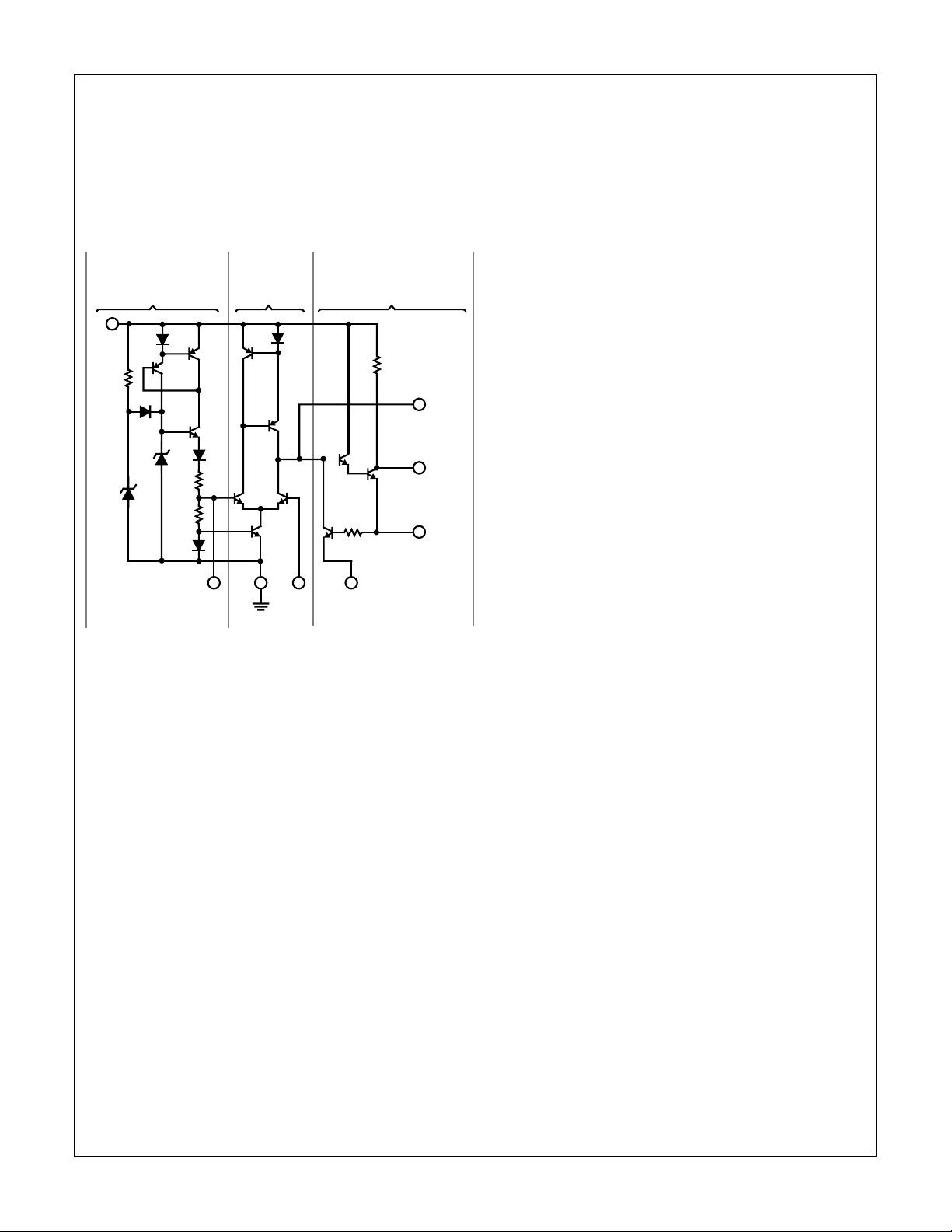
Brief Description of CA3085 Schematic Diagram
The schematic diagram of the CA3085 series circuits is
shown in Figure 2. The left-hand section includes the starting circuit, the voltage reference circuit, and the constantcurrent circuit. The center section is basically an elementary
operational amplifier which serves as the voltage-error
EXTERNAL INHIBIT
CURRENT
BOOSTER
SERIES
PASS
AMPL.
CURRENT
LIMITING
2 7
CURRENT
LIMITING
1
OUTPUT
REGULATED
Copyright © Harris Corporation 1992
11-52

Application Note 6157
amplifier controlling the series-pass. Darlington pair (Q13,
Q14) shown in the right-hand section when controlled by an
appropriate external sensing network, transistor Q15, serves
to provide protective current-limiting characteristics by
diverting base drive from the series pass circuit. For operation at the highest current levels, terminals 2 and 3 are tied
together to eliminate the voltage drop which would otherwise
be developed across resistor R5.
VOLTAGE-REFERENCE,
STARTUP AND
CONSTANT-CURRENT
CIRCUITS
3
V+IN
UNREG.
INPUT
R
1
40k
D
1
ALL RESISTANCE VALUES
ARE IN Ω
D
6
Q
1
D
2
D
3
R
2
4k
R
3
1.5k
D
5
V
REF
FIGURE 2. SCHEMATIC DIAGRAM OF CA3085 SERIES
Q
2
Q
3
D
4
5
VOLTAGE-
ERROR
AMP (OP AMP)
Q
8
Q
Q
Q
6
5
Q
4
4
V-
INV.
INPUT
SUBSTRATE
SERIES-PASS AND CURRENT-
LIMITING CIRCUITS
D
7
R
5
500
R
1.5k
Q
13
4
8
COMPENSATION
AND EXTERNAL
INHIBIT
Q
14
REGULATED
9
6
Q15
CURRENT
LIMITING
7
2
CURRENT
BOOSTER
1
OUTPUT
Voltage Reference Circuits
The basic voltage referenced element used in the CA3085 is
zener diode D3. It provides a nominal reference voltage of
5.5V and exhibits a positive temperature coefficient of
approximately 2.5mV/
o
C. If this reference voltage were used
directly in conjunction with the error-amplifier (Q5, Q6, etc.),
the IC would exhibit two major undesirable characteristics:
(1) its performance with temperature variations would be
poor, and (2) its use as a regulator would be restricted to circuits in which the minimum regulated output voltages are in
excess of 5.5V. Consequently, it is necessary to provide
means of compensating for the positive temperature coefficient of D3 and at the same time provide for obtaining a stable source of lower reference voltage. Both temperature
compensation and the reduction of the reference voltage are
accomplished by means of the series divider network consisting of the base-emitter junction of Q3, diode D4, resistors
R2 and R3, and diode 5.
The voltage developed across D3 drives the divider network
and a voltage of approximately 4V is developed between the
cathode of D4 and the cathode of D5 (terminal 4). The current through this divider network is held nearly constant with
temperature because of the combined temperature coefficients of the zener diode (D3), Q3 base-emitter junction, D4,
D5, and the resistors R2 and R3. This constant current
through the diode D5 and the resistor R3 produces a voltage
drop between terminals 4 and 5 that results in the reference
voltage (≈ 1.6V) having an effective temperature coefficient
of about 0.0035%/
o
C.
The reference diode D3 receives a currant of approximately
620µA from a constant-current circuit consisting of Q3 and
the current-mirror* D6, Q1, and Q2. Current to start-up the
constant-current source initially is provided by auxiliary
zener diode D1 and R1. Diode D2 blocks current from the
R1-D1 source after latch-in of the constant-current source
establishes a stable reference potential, and thereby prevents modulation of the reference voltage by ripple voltage
on the unregulated input voltage.
Voltage-Error Amplifier
Transistors Q5 and Q6 comprise the basic differential amplifier that is used as a voltage-error amplifier to compare the
stable reference voltage applied at the base of Q5 with a
sample of the regulator output voltage applied at terminal 6.
The D5-Q4 combination is a current-mirror which maintains
essentially constant-current flow to Q5 and Q6 despite variations in the unregulated input voltage. The Q8, Q9, and D7
network provides a “mirrored” active collector load for Q5
and Q6 and also provides a variable single-ended drive to
the Q13 and Q14 series-pass transistors in accordance with
the difference signal developed between the bases of Q5
and Q6. The open-loop gain of the error-amplifier is greater
than 1000.
Series-Pass and Current-Limiting Circuits
In the normal mode of operation, or in the current-boost
mode when terminals 2 and 3 are tied together, the Darlington pair Q13-Q14 performs the basic series-pass regulating
function between the unregulated input voltage and the regulated output voltage at terminal 1. In the current-limiting
mode transistor Q15 provides current-limiting to protect the
CA3085 and/or limit the load current. To provide current-limiting protection, a resistor (e.g., 5Ω) is connected between
terminals 1 and 8; terminal 8 becomes the source of regulated output voltage. As the voltage drop across this resistor
increases, base drive is supplied to transistor Q15 so that it
becomes increasingly conductive and diverts base drive
from the Q13-Q14 pass transistor to reduce output current
accordingly. Resistor R4 is provided to protect Q15 against
overdrive by limiting its base current under transient and
load-short conditions.
Because the CA3085 regulator is essentially an op-amp
having considerable feedback, frequency compensation
may be required to prevent oscillations. Stability must also
be maintained despite line and load transients, even during
operation into reactive loads (e.g., filter capacitors). Provisions are included in the CA3085 so that a small-value
capacitor may be connected between terminals 6 and 7 to
compensate the regulator, when necessary, by “rolling-off”
the amplifier frequency-response. Terminal 7 is also used to
externally “inhibit” operation of the CA3085 by diverting base
current supplied to Q13-Q14, thereby permitting the use of
keying, strobing, programming, and/or auxiliary overloadprotection circuits.
11-53

Application Note 6157
Applications
A Simple Voltage Regulator
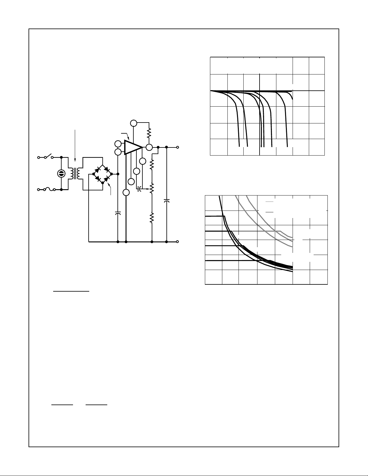
Figure 3 shows the schematic diagram of a simple regulated
power supply using the CA3085. The ac supply voltage is
stepped down by T1, full-wave rectified by the diode bridge
circuit, and smoothed by the large electrolytic capacitor C1
to provide unregulated dc to the CA3085 regulator circuit.
Frequency compensation of the error-amplifier is provided
by capacitor C2. Capacitor C3 bypasses residual noise in
the reference-voltage source, and thus decreases the incremental noise-voltage in the regulator circuit output.
TI: STANCOR TP3
CA3085, A, B
BLACK
WHITE
GREEN
120V
60Hz
BLACK
RED
(4)
1N3193
500µF
50V
+
-
FIGURE 3. BASIC POWER SUPPLY
Because the open-loop gain of the error-amplifier is very
high (greater than 1000), the output voltage may be directly
calculated from the following expression:
V
O
(R2 + R1)
=
R1
V
REF
1
5.6Ω
V
2
3
5
4
8
6
7
OUT
8.2
KΩ
10
KΩ
5µF
35V
1
KΩ
(EQ. 1)
The line-and-load regulation characteristics for the circuit
shown in Figure 3 are approximately 0.05 percent of the output voltage.
INPUT VOLTAGE (V+I) = 15V
OUTPUT VOLTAGE (V+
AMBIENT TEMPERATURE (T
O
0
-0.1
-0.2
-0.3
LOAD REGULATION - % V
+
-0.4
0 20 40 60 80 100
20Ω
FIGURE 4. LOAD REGULATION CHARACTERISTICS FOR
CIRCUIT OF FIGURE 3
)
OUT
- V
IN
25
20
-
15
10
5
0
0 20406080100
INPUT VOLTS MINUS OUTPUT VOLTS (V
40V
25V
20V
) = 10V
O
) = 25oC
A
9Ω
10Ω
15Ω
LOAD CURRENT (I
15V
OUTPUT (mA)
RSC = 0
5Ω
6Ω
8Ω
) - mA
L
OPERATION WITHOUT
HEAT SINK
OPERATION WITH
HEAT SINK
INPUT VOLTS
(VIN) = 20V
40V
50V
INPUT VOLTS
(VIN) = 10V
In the circuit shown in Figure 3, the output voltage can be
adjusted from 1.8V to 20V by varying R2. The maximum output current is determined by R
istics for various values of R
; load-regulation character-
SC
are shown in Figure 4.
SC
When this circuit is used to provide high output currents at
low output voltages, care must be exercised to avoid excessive IC dissipation. In the circuit of Figure 3, this dissipation
control can be accomplished by increasing the primary-tosecondary transformer ratio (a reduction in V
) or by using a
I
dropping resistor between the rectifier and the CA3085 regulator. Figure 5 gives data on dissipation limitation (V
I
) for CA3085 series circuits. The short-circuit current is
O
- VO vs.
I
determined as follows:
ISC =
V
BE
R
SC
0.7
≈
R
amperes (EQ. 2)
SC
FIGURE 5. DISSIPATION LIMITATION (V
- VO vs IO) FOR
I
CA3085 SERIES CIRCUITS
High-Current Voltage Regulator
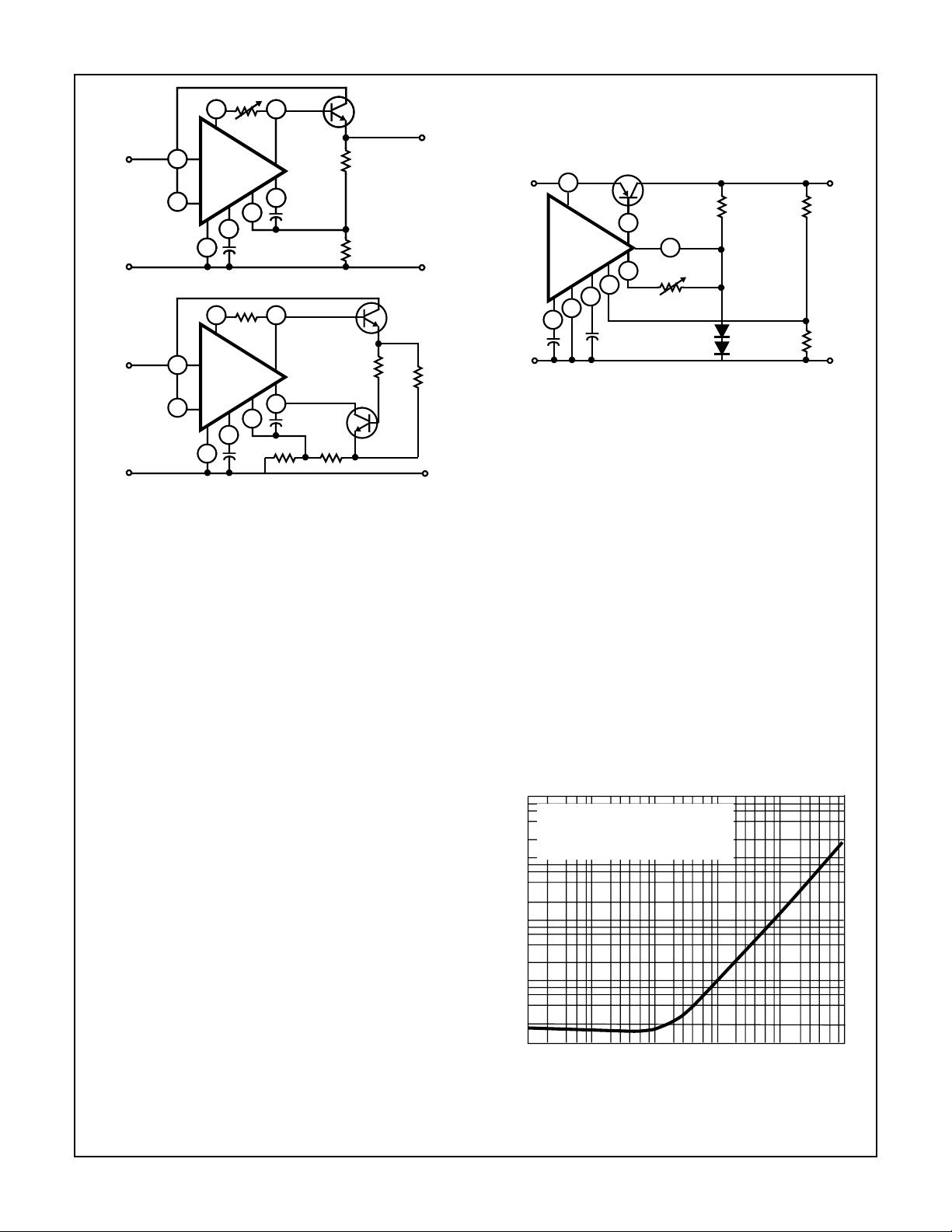
When regulated voltages at currents greater than 100mA are
required, the CA3085 can be used in conjunction with an
external n-p-n pass transistor as shown in the circuits of Figure 6. In these circuits the output current available from the
regulator is increased in accordance with the h
external n-p-n pass transistor. Output currents up to 8A can
be regulated with these circuits. A Darlington power transistor can be substituted for the 2N5497 transistor when currents greater than 8A are to be regulated.
11-54
of the
FE

Application Note 6157
R
R
SCP
SCP
1 8
1 8
2
+
+
UNREG.
UNREG.
V
V
-
-
2
CA3085
CA3085
7
2µF
2µF
7
6
6
0.001µF
0.001µF
3
3
I
I
5
5
+
4
4
FIGURE 6A. WITH SIMPLIFIED SHORT-CIRCUIT PROTECTION
R3
1 8
6.8Ω
+
UNREG.
V
2
CA3085
2µF
7
6
0.001µF
R1
3
I
5
+
4
-
FIGURE 6B. WITH AUXILLIARY SHORT-CIRCUIT PROTECTION
FIGURE 6. HIGH-CURRENT VOLTAGE REGULATOR USING
n-p-n PASS TRANSISTOR
A simplified method of short circuit protection is used in connection with the circuit of Figure 6A. The variable resistor
R
serves two purposes: 1) it can be adjusted to optimize
SCP
the base drive requirements (h
) of the particular 2N5497
FE
transistor being used, and 2) in the event of a short circuit in
the regulated output voltage the base drive current in the
2N5497 will increase, thereby increasing the voltage drop
across R
. As this voltage drop increases the short circuit
SCP
protection system within the CA3085 correspondingly
reduces the output current available at terminal 8, as
described previously. It should be noted that the degree of
short circuit protection depends on the value of R
design compromise is required in choosing the value of
R
to provide the desired base drive for the 2N5497 while
SCP
maintaining the desired short circuit protection. Figure 6B
shows an alternate circuit in which an additional transistor
(2N2102) and two resistors have been added as an auxiliary
short circuit protection feature. Resistor R3 is used to establish the desired base drive for the 2N5497, as described
above. Resistor R
now controls the short circuit output
LIMIT
current because, in the event of a short circuit, the voltage
drop developed across its terminals increases sufficiently to
increase the base drive to the 2N2102 transistor. This
increase in base drive results in reduced output from the
CA3085 because collector current flow in the 2N2102 diverts
base drive from the Darlington output stage of the CA3085
(see Figure 2) through terminal 7. The load regulation of this
circuit is typically 0.025 per cent with 0 to 3A load-current
variation; line regulation is typically 0.025%/V change in
input voltage.
Voltage Regulator with Low V
- VO Difference
I
In the voltage regulators described in the previous section, it
is necessary to maintain a minimum difference of about 4V
R2
R2
R1
R1
R2
2N5497
2N5497
1KΩ
2N5183
REG.
REG.
V
V
O
O
2N5497
SCP
+
+
-
-
R
LIMIT
REG.
-
, i.e.,
V
O
between the input and output voltages. In some applications
this requirement is prohibitive. The circuit shown in Figure 7
can deliver an output current in the order of 2A with a V
- V
I
difference of only one volt.
2N4036
+
7
UNREG.
V
I
2µF
-
CA3085
4
5
Q1
2
8
1
6
7
R
SCP
10KΩ
D1
D2
IN914’s
FIGURE 7. VOLTAGE REGULATOR FOR LOW VI - V
+
R2
REG.
V
O
R1
-
O
DIFFERENCE
It employs a single external p-n-p transistor having its base
and emitter connected to terminals 2 and 3, respectively, of
the CA3085. In this circuit, the emitter of the output transistor
(Q14 in Figure 2) in the CA3085 is returned to the negative
supply rail through an external resistor (R
) and two
SCP
series-connected diodes (D1, D2). These forward biased
diodes maintain Q6 in the CA3085 within linear-mode operation. The choice of resistors R1 and R2 is made in accordance with Equation 1. Adequate frequency compensation
for this circuit is provided by the 0.01µF capacitor connected
between terminal 7 of the CA3085 and the negative supply
rail.
Figure 8 which shows the output impedance of the circuit of
Figure 7 as a function of frequency, illustrates the excellent
ripple-rejection characteristics of this circuit at frequencies
below 1kHz. Lower output impedances at the higher frequencies can be provided by connecting an appropriate
capacitor across the output voltage terminals. The addition
of a capacitor will, however, degrade the ability of the system
to react to transient-load conditions.
1000
INPUT VOLTAGE (V+I) = 15V
OUTPUT VOLTAGE (V+
AMBIENT TEMPERATURE (T
100
10
1
OUTPUT RESISTANCE (Ω)
0.1
0.01 0.1 1 10 100 1000
FIGURE 8. OUTPUT RESISTANCE vs FREQUENCY FOR
CIRCUIT OF FIGURE 7
) = 10V
O
) = 25oC
A
FREQUENCY (kHz)
O
11-55
 Loading...