Harris Semiconductor CA3018A, CA3018 Datasheet

SEMICONDUCTOR
CA3018
March 1993
Features
• Matched Monolithic General Purpose Transistors
Matched . . . . . . . . . . . . . . . . . . . . . . . . . . . . . . . . . .±10%
•h
FE
Matched
•V
BE
- CA3018A . . . . . . . . . . . . . . . . . . . . . . . . . . . . . . . . . . ±2mV
- CA3018. . . . . . . . . . . . . . . . . . . . . . . . . . . . . . . . . . . . ±5mV
• Operation From DC to 120MHz
• Wide Operating Current Range
• CA3018A Performance Characteristics Controlled
from 10µA to 10mA
• Low Noise Figure. . . . . . . . . . . . .3.2dB Typical at 1kHz
• Full Military Temperature Range . . . . -55
o
C to +125oC
Applications
• Two Isolated Transistors and a Darlington Connected
Transistor Pair for Low Power Applications at
Frequencies from DC through the VHF Range
• Custom Designed Differential Amplifiers
• Temperature Compensated Amplifiers
• See Application Note, AN5296 “Application of the
CA3018 Integrated Circuit Transistor Array” for
Suggested Applications
General Purpose Transistor Arrays
Description
The CA3018 and CA3018A consist of four general purpose
silicon n-p-n transistors on a common monolithic substrate.
Two of the four transistors are connected in the Darlington
configuration. The substrate is connected to a separate
terminal for maximum flexibility.
The transistors of the CA3018 and the CA3018A are well
suited to a wide variety of applications in low power systems
in the DC through VHF range. They may be used as discrete
transistors in conventional circuits but in addition they
provide the advantages of close electrical and thermal
matching inherent in integrated circuit construction.
The CA3018A is similar to the CA3018 but features tighter
control of current gain, leakage, and offset parameters
making it suitable for more critical applications requiring
premium performance.
Ordering Information
PART
NUMBER
CA3018 -55oC to +125oC 12 Pin CAN
CA3018A -55oC to +125oC 12 Pin CAN
TEMPERATURE
RANGE PACKAGE
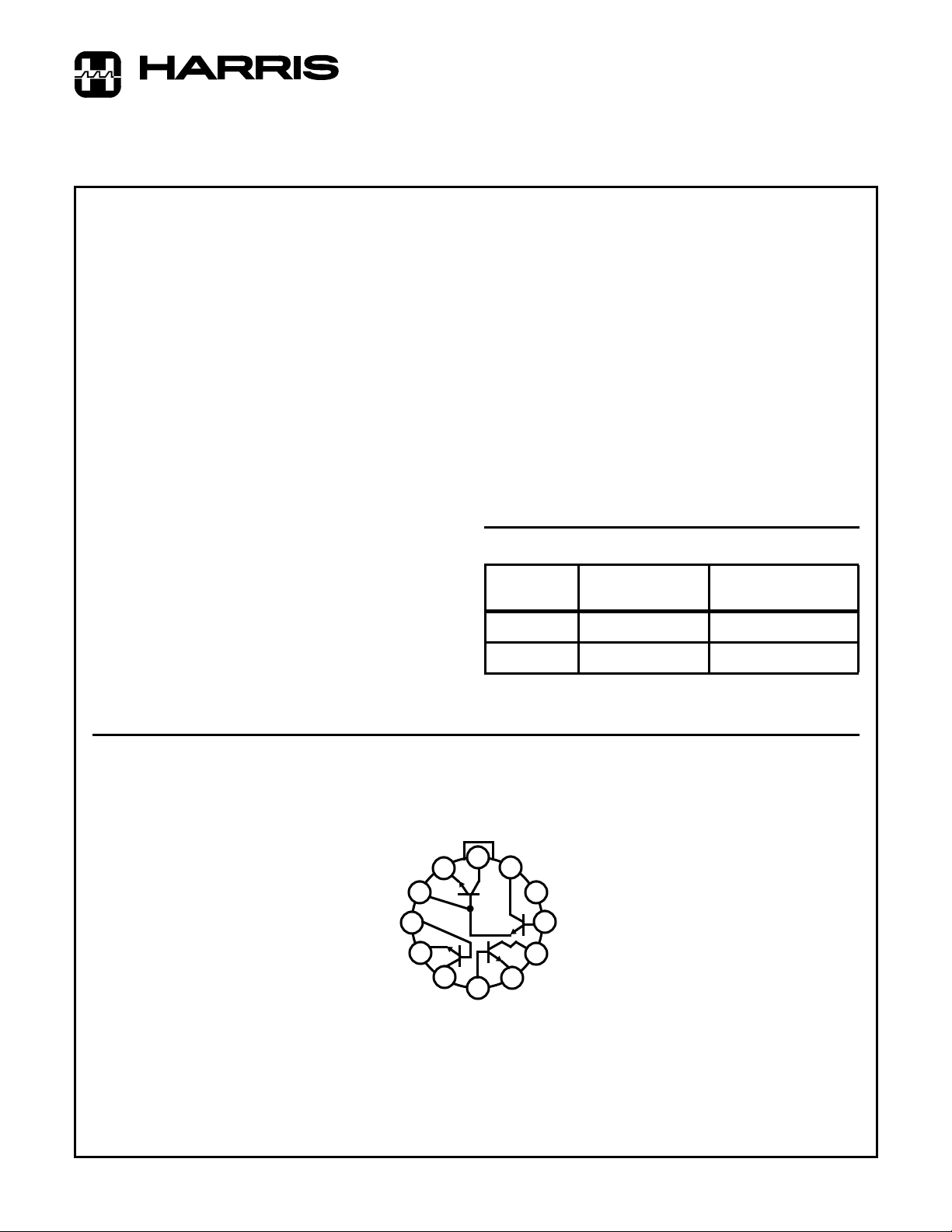
Pinout
CA3018, CA3018A
(TO-5 CAN)
TOP VIEW
12
Q4
6-5
11
SUBSTRATE
10
9
Q3
Q1
8
7
6
1
2
3
4
Q2
5
CAUTION: These devices are sensitive to electrostatic discharge. Users should follow proper I.C. Handling Procedures.
Copyright
© Harris Corporation 1993
File Number 338.2

Specifications CA3018, CA3018A
Absolute Maximum Ratings (T
Collector-to-Emitter Voltage, V
Collector-to-Base Voltage, V
Collector-to-Substrate Voltage, V
Emitter-to-Base Voltage, V
CEO
CBO
. . . . . . . . . . . . . .5V 5V
EBO
= +25oC) Operating Conditions
A
CA3018 CA3018A
. . . . . . . . . . .15V 15V
Operating Temperature Range . . . . . . . . . . . . -55oC ≤ TA≤ +125oC
Storage Temperature Range. . . . . . . . . . . . . . -65oC ≤ TA≤ +150oC
. . . . . . . . . . . .20V 30V
(Note 1) . . 20V 40V
CIO
Collector Current, IC. . . . . . . . . . . . . . . . . . . . . .50mA 50mA
Power Dissipation
Any One Transistor. . . . . . . . . . . . . . . . . . . . . . . . . . . . . . 300mW
Total Package . . . . . . . . . . . . . . . . . . . . . . . . . . . . . . . . . . 450mW
TA > +85oC . . . . . . . . . . . . . . . . . . . . . . . . . . . .Derate at 5mW/oC
Junction Temperature. . . . . . . . . . . . . . . . . . . . . . . . . . . . . . +175oC
Lead Temperature (Soldering 10 Sec.). . . . . . . . . . . . . . . . . +300oC
CAUTION: Stresses above those listed in “Absolute Maximum Ratings” may cause permanent damage to the device. This is a stress only rating and operation
of the device at these or any other conditions above those indicated in the operational sections of this specification is not implied.
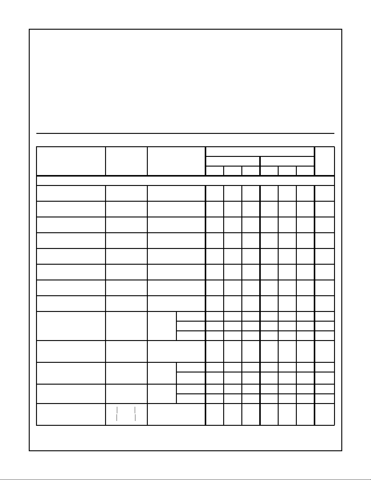
Electrical Specifications T
= +25oC
A
LIMITS
CA3018 CA3018A
PARAMETERS SYMBOL TEST CONDITIONS
MIN TYP MAX MIN TYP MAX
UNITS
STATIC CHARACTERISTICS
Collector Cutoff Current
I
CBO
VCB = 10V, IE = 0 - 0.002 100 - 0.002 40 nA
(Figure 1)
Collector Cutoff Current
(Figure 2)
Collector Cutoff Current
I
CEO
I
CEOD
VCE = 10V, IB = 0 - See
Fig. 2
5 - See
Fig. 2
0.5 µA
VCE = 10V, IB = 0 -----5µA
Darlington Pair
Collector-to-Emitter
V
(BR)CEO
IC = 1mA, IB = 0 15 24 - 15 24 - V
Breakdown Voltage
Collector-to-Base Breakdown
V
(BR)CBO
IC = 10µA, IE = 0 20 60 - 30 60 - V
Voltage
Emitter-to-Base Breakdown
V
(BR)EBO
IE = 10µA, IC = 0 5 7 - 5 7 - V
Voltage
Collector-to-Substrate
V
(BR)CIO
IC = 10µA, ICI = 0 20 60 - 40 60 - V
Breakdown Voltage
Collector-to-Emitter
V
CES
IB = 1mA, IC = 10mA - 0.23 - - 0.23 0.5 V
Saturation Voltage
Static Forward Current
Transfer Ratio (Note 2)
(Figure 3)
h
FE
VCE = 3V IC = 10mA - 100 - 50 100 - -
IC = 1mA 30 100 200 60 100 200 IC = 10µA - 54 - 30 54 - -
Magnitude of Static-Beta
Ratio (Isolated Transistors Q
1
VCE = 3V,
IC1 = IC2 = 1mA
0.9 0.97 - 0.9 0.97 - -
and Q2) (Figure 3)
Static Forward Current
Transfer Ratio Darlington Pair
(Q3 and Q4) (Figure 4)
Base-to-Emitter Voltage
(Figure 5)
Input Offset Voltage
(Figures 5, 7)
h
V
V−
FED
V
BE1
BE2
BE
VCE = 3V IC = 1mA 1500 5400 - 2000 5400 - -
IC = 100µA - - - 1000 2800 - -
VCE = 3V IE = 1mA - 0.715 - 0.600 0.715 0.800 V
IE = 10mA - 0.800 - - 0.800 0.900 V
VCE = 3V, IE = 1mA - 0.48 5 - 0.48 2 mV
6-6
 Loading...