

Maintenance Manual
LBI-38641F
VHF RECEIVER SYNTHESIZER MODULE
19D902781G1 & G2
TABLE OF CONTENTS
Page
DESCRIPTION . . . . . . . . . . . . . . . . . . . . . . . . . . . . . . . . . . . . . . . . . . . . Front Cover
GEN ERAL S PECIFIC ATIONS . . . . . . . . . . . . . . . . . . . . . . . . . . . . . . . . . . . . . 1
CIRCUIT ANALYSIS . . . . . . . . . . . . . . . . . . . . . . . . . . . . . . . . . . . . . . . . . . 2
VOLTAGE CONTROLLED OSCILLATOR . . . . . . . . . . . . . . . . . . . . . . . . . . . . 2
BUFFER AMPLIFIERS . . . . . . . . . . . . . . . . . . . . . . . . . . . . . . . . . . . . . . . 2
REFERENCE OSCILLATOR AND BUFFER . . . . . . . . . . . . . . . . . . . . . . . . . . . 2
PRESCALER AND SYNTHESIZER . . . . . . . . . . . . . . . . . . . . . . . . . . . . . . . . 2
LOOP FILTER . . . . . . . . . . . . . . . . . . . . . . . . . . . . . . . . . . . . . . . . . . . . 2
DIGITAL CONTROL . . . . . . . . . . . . . . . . . . . . . . . . . . . . . . . . . . . . . . . . 2
VOLTAGE REGULATORS . . . . . . . . . . . . . . . . . . . . . . . . . . . . . . . . . . . . . 2
MAINTENANCE . . . . . . . . . . . . . . . . . . . . . . . . . . . . . . . . . . . . . . . . . . . . . 3
TEST AND ALIGNMENT PROCEDURE . . . . . . . . . . . . . . . . . . . . . . . . . . . . . 3
TROUBLESHOOTING . . . . . . . . . . . . . . . . . . . . . . . . . . . . . . . . . . . . . . . 3
ASSEMBLY DIAGRAM . . . . . . . . . . . . . . . . . . . . . . . . . . . . . . . . . . . . . . . . . 4
OUTLINE DIAGRAM . . . . . . . . . . . . . . . . . . . . . . . . . . . . . . . . . . . . . . . . . . 5
SCH EMATIC DIAGRAM . . . . . . . . . . . . . . . . . . . . . . . . . . . . . . . . . . . . . . . . 6
PARTS LIST . . . . . . . . . . . . . . . . . . . . . . . . . . . . . . . . . . . . . . . . . . . . . . . . 12
PRODUCTION CHANGES . . . . . . . . . . . . . . . . . . . . . . . . . . . . . . . . . . . . . . . 13
IC DATA . . . . . . . . . . . . . . . . . . . . . . . . . . . . . . . . . . . . . . . . . . . . . . . . . . 13
DESCRIPTION
The Receiver Synthesizer Module provides the local
oscillator signal (LO) to the Receiver Front End Module
of the MASTR III base stati on. T he m odule a lso provide s
the reference oscillator signal to the transmitter synthesizer. Receiver Synthesizer Module 19D902781G1
(Group 1) generates an output injection signal in the 157
to 172 MHz range, and 19D902781G2 (Group 2) generates a signal in the 129 to 152 MHz Range.
The Receiver Synthesizer Module is a phase-locked
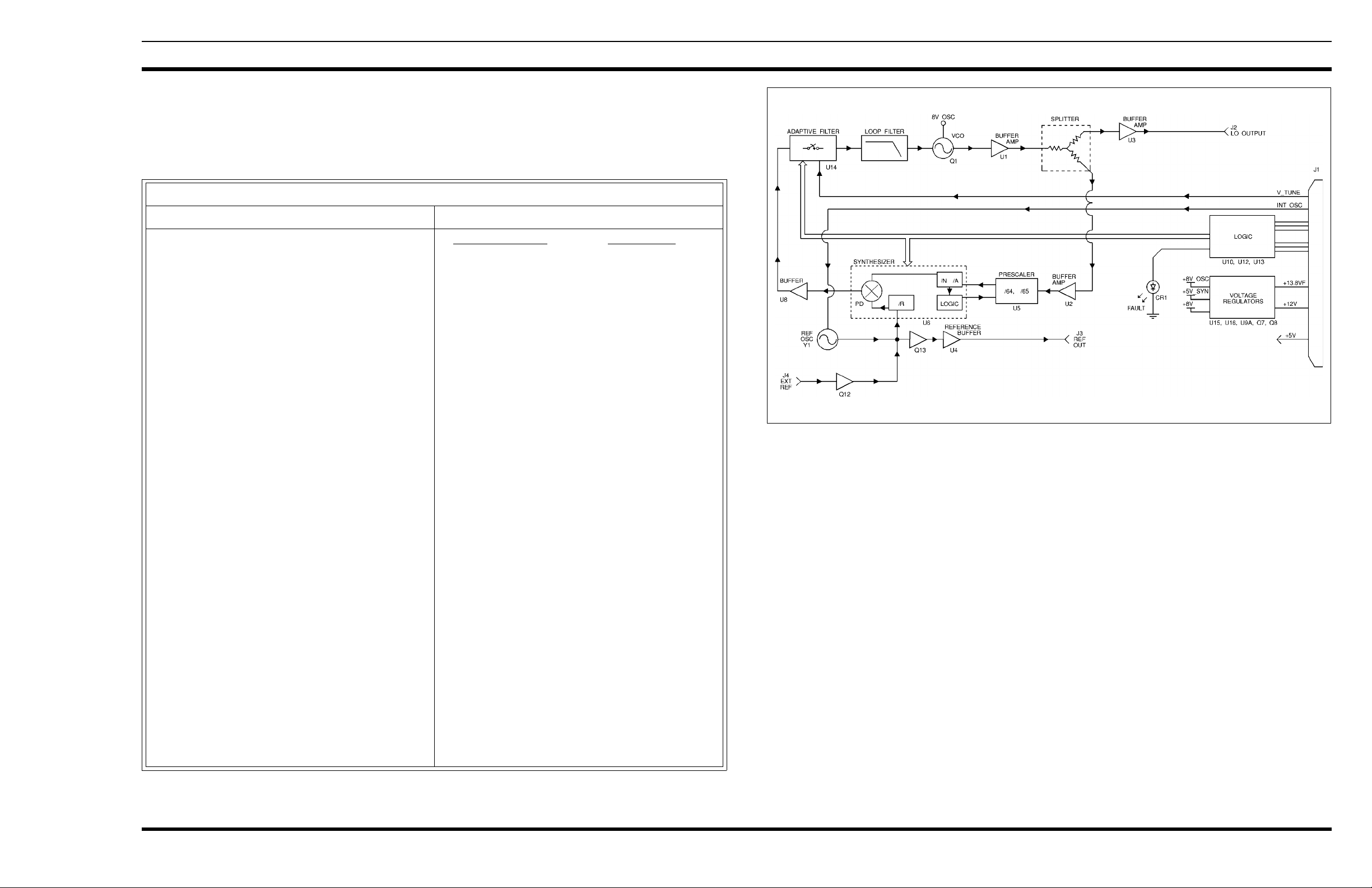
loop (PLL) design, as shown in the block diagram (Figure
1). Its output is generated directly by the VCO Q1 and
buffered by Monolithic Microwave Integrated Circuits
(MMIC) U1 and U3.
The logic signals from controller (U10, 12, and 13)
determine the synthesizer frequency. Frequency stability
is maintained by either using the internal reference oscil-
lator Y1 or by applying a high precision reference signal
to the EXT Reference Oscillator Port J4. The internal
reference oscillator is a temperature controlled crystal
oscillator (TCXO) operating at 12.8 MHz. The oscillator
has a stability of ±1.5 ppm over the temperature range of
-30°C to +75°C. See the table co nta inin g G ene ra l Spec ifications for the minimum external oscillator specifications.
The buffered VCO output is sampled by the resistive
splitter and conditioned by buffer amplifie r U2 . I t is th en
fed to the divide by 64/65 dual modulus prescaler U5. T he
divided output from the prescaler is connected to the F
input of the PLL U6. Within the PLL the divided VCO
input signal F
down the 12.8 MHz reference signal. Three inputs from
the controller; ENABLE, CLOCK, and serial DATA program the PLL divider circuits.
is divided again. The PLL also divides
in
in
M/A-COM Wireless Systems
3315 Old Forest Road
Lynchburg, Virgini a 24 50 1
(Outside USA, 434-385-2400) Toll Free 800-528-7711
macom-wireless.com Printed in U.S.A.
www.
LBI-38641F
The divided reference signal and the divided VCO signal
are compared in the PLL phase detect or. When the reference
and VCO signals are identical the PLL phase detector g enerates
a constant DC output voltage. This voltage is buffered by U8
and filtered by the loop filter circuit. It is then applied to Q1
setting the VCO on frequency.
TABLE 1 - GENERAL SPECIFICATIONS
ITEM SPECIFICATION
FREQUENCY TUNING
Output Injection Signal
Electrical
Full Specifications
Degraded Specifications
Channel Spacing
FREQUENCY STABILITY
LO POWER OUTPUT
LO NOMINAL IMPEDANCE 50 Ohms
If the compared frequencies (phases) differ, an error voltage
is generated which adjusts the VCO frequency. During this
out-of-lock condition, the PLL also sends a Lo ck Detect sig nal
(LD) to the controller and lights the FAULT LED on the front
panel of the module.
INJECTION FREQ. FREQ. BAND
157.4 MHz - 172.2 MHz (G1) 136 MHz - 150.8 MHz
129.4 MHz - 152.6 MHz (G2) 150.8 MHz - 174 MHz
2 MHz
3 MHz
5 kHz
±
1.5 ppm
1.5 dBm ±1.5 dBm
PHASE NOISE
@ 25 kHz Offset
@ 30 kHz Offset
HUM AND NOISE
Companion Receiver -60 dB
HARMONICS @ LO PORT <-30 dBc
SWITCHING SPEED < 50 ms
CURRENT DRAIN
+13.8V
+12V
REFERENCE OSCILLATOR
Frequency Output
Power Output
Impedance
EXT. REFERENCE OSCILLATOR
Frequency Output
Power Output
Impedance
-142 dBc/Hz
-147 dBc/Hz
<200 mA
<50 mA
12.8 MHz ±1.5 ppm
0 dBm ±1.5 dBm
50 ohms
5.00 MHz to 17.925 MHz (must be divisible by the
channel spacing)
10 dBm ±3 dBm into 50 ohms
50 ohms
Figure 1 - Receiver Synthesizer Block Diagram
CIRCUIT ANALYSIS
The Receiver Synthesizer Module consists of the follow-
ing circuits:
Voltage Controlled Oscillator
•
Buffer Amplifiers
•
Reference Oscillator and Buffer
•
Prescaler and Syn the size r
•
Loop Filter
•
Digital Control
•
Voltage Regulators
•
VOLTAGE CONTROLLED OSCILLATOR
The free running Voltage Controlled Osc illator (VCO) is
composed of a grounded-gate JFET (Q1) and associated
circuitry. Inductor L10 and associated capacitors form the
resonant tank c ircuit. The circ uit’ s use of high-Q components
minimizes phase noise.
Frequency tunin g of the VCO is don e by changing the
DC output voltage level from the loop filter U14. The Loop
Filter Out signal from U14 is routed through L4 and R3 a nd
applied to the two varicap diodes D4 and D5. The voltage
level applied determines the diodes’ capacitance and sets the
resonant frequency of the oscillator . If the VCO drifts or the
frequency is cha nged, th e DC vo ltage le vel ch ange s c ausing
the VCO’s resonant frequency to change. The output of the
oscillator is then applied to a buffer amplifier . Course adjustment of freque ncy is done by adjusting tri mmer capacitor
C52 while applying a calibration voltage to the V_TUNE
line connected to U14.4-11.
BUFFER AMPLIFIERS
The MMIC Buffer Amplifier stage is composed of three
MMICs (U1, U2, and U3) and a resistive splitter . T he amplifiers serve two purposes; amplifying the local oscillator
signal (LO OUTPUT) for injection into the Receiver Front
End assembly and providing a feedback signal to the synthesizer Phase-Locked Loop (PLL).
Copyright© 1992-2002, M/A-COM Private Radio Systems, Inc. All rights reserved.
1

LBI-38641F
Integrated circuits U1 and U3 provide amplification of
the local oscillator signal. The output of U1 is fed to a
resistive signal splitter composed of R13 through R18. One
of the resistive signal splitter outputs drives amplifier U3.
The U3 output signal is coupled by C17 to a low-pass filter
network (C24 and C25, L6, L8, and L9) and a resistive pad
(R25, R26 and R30) for isolation. The local oscillato r signal
is finally routed to J2, LO OUT, for connection to the
Receiver Front End Assembly. The LO output level at BNC
connector J2 is nominally 0 dBm.
The other output of the resistive signal splitter drives U2.
The amplified output from U2, PRESCALER BUFFER
OUT, is coupled to the 50 ohm input of the prescaler U5 via
capacitors C16 and C45.
REFERENCE OSCILLATOR AND BUFFER
The reference oscillator section provides a reference
signal to the PLL section. The circuit design allows using
either an external or internal oscillator.
When using an external oscillator, the internal oscillator
is disabled by placing a logic low on the INT OSC line from
the T/R Shelf Interface Board. A high precision external
oscillator may then be connected to the module through the
external reference oscillator connector J4, EXT REF IN. J4
has a 50 ohm input impedance and is coupled to the base of
Q12. Buffer Q12 conditions the signal and applies it to the
synthesizer U6 via coupling capacitor C10.
The internal reference oscillator, Y1, provides a 12.8
MHz signal with a stability of ±1.5 ppm. It i s enabled by
applying a logic high signal on the INT OSC line . This signa l
turns on Q2, allowing it to conduct and apply +5 volts to pin
1 of the oscillator Y1. The 12.8 MHz output signal (Y1 pin
2) is then sent to the synthesizer via coupling capacitor C9.
The reference oscillator signal, either external or internal, is also routed to Q13 via coupling capacitor C54. The
output taken from the emitter of Q13 is applied through C11
to the input of Buffer Amplifier U4. The buffered signal is
coupled through C12 to a low pass filter network
(C32,C33,C3 4, and L 7) and a re sistive pa d (R27, R28, and
R31) for isolation. The output from the resistive pad is then
connected to J3, REF OUT, making the reference oscillator
signal available for external use.
PRESCALER AND SYNTHESIZER IC
The integrated circuit U6 is the heart of the synthesizer.
It contains the necessary frequency dividers and control
circuitry to synthesize output frequencies by the technique
of dual modulus prescaling. U6 also contains an analog
sample and hold ph ase dete cto r an d a loc k de tec tor circ uit.
Within the U6 are three programmable dividers which
are serially loaded us ing the C LOCK, DATA, and ENABLE
inputs (pins 11, 12, and 13 respectively). A ser ial data stream
(DATA) on pin 12 is shifted into the internal shift registers
by low to high transitions on the clock input (CLOCK) at pin
11. A logic high (ENABLE) on pin 13 then transfers the
program information from the shif t registers to the divider
latches. The serial data determines the VCO frequency by
setting the internal R, A, and N dividers.
The 12.8 MHz reference oscillator signal OSCIN is internally r outed to the " R" divider. The "R" div ider divides
down the 12.8 MHz reference signal to a lower frequency,
F
, as directed by the input data and applies the signal to the
r
internal analog phase and lock detectors.
The "A" and "N" dividers process the loop feedback
signal from the VCO (by way of the dual modulus prescaler
U5). The out put of the " N" divider, F
version of the VCO output frequency. This signal is also
applied to the internal phase detector. The ramp and hold
constants are determined by C26, R37, C31, and R36.
The analog phase detector output voltage (PD OUT) is
proportional to the phase difference between F
output serves as the loop error signal. When operating on the
correct frequency, the inputs to the phase detector are identical and the output voltage of the analog phase detector is
constant. If the compared frequencies (phases) differ, the
analog phase detector increases or decreases the DC output
voltage (PD OUT). This error signal voltage tunes the VCO
to whatever freque ncy is r equir ed to k eep F
(in phase).
The lock detector furnishes the Fault circuit in U13 with
the lock detect (LD) signal. When F
lock detector output sends a logic high on the LD line to the
fault circuit U13. If the VCO is not locked onto the correct
frequency, the resulting out-of-phase condition causes the
output from the lock detector to be a logic low.
, is a divided down
v
and Fr. This
v
and Fr locked
v
and Fr are in phase, the
v
LOOP FILTER
The error signal, ANOUT, is applied to the loop filter at
U8.2-5 and U8.1-3. U8.2 ac ts as a buff er amplifier with gain.
The output signal from the amplifie r is applied to a loop f ilter
consisting of R42, R43, R44, C35 and C36 via the bilateral
switch U14. The filter removes noise and sa mpling frequencies from the error voltage. The switch, U14, selects the
proper filter configuration for operation in the narrow band,
wide band or tuning mode. The control signals
(OPEN_LOOP, ENABLE_NOT, and TUNE_CTRL) for
U14 are derived from the digital control cir cuits U10, U12, and
U13. U8.1 provides a buffered output for testing at the DIN
connector on the rear of the module.
DIGITAL CONTROL
Logic control circuits (other than those inside the synthe-
sizer IC - U6) consist of the following:
Digital Control Circuit (U10, U12, & U13)
•
Level Shifters
•
Fault Circuit
•
The Digital Control Circuits U10, U12, & U13 serve as an
interface between the controller and the synthesizer IC.
As an address decoder, U10 enables the input gates when
the A0, A1, and A2 input lines (pins 4, 3, and 2) receive the
correct address code from the controller. For the Receiver
synthesizer the enable address is 010 on A0, A1, and A2
respectively. After receiving the proper logic code, the input
gate U12 is enabled. This allows the ENABLE, CLOCK, and
serial DATA information to pass on to the synthesizer via the
level shifters.
The Level Shifters Q3, Q4, and Q5 convert the five (5) vo lt
logic level to the eight (8) volt logic level required by the
synthesizer.
The Fault circuit, U13, monitors the lock detect signal from
the PLL synthesizer . Under normal (locked) condition, the PLL
sends a logic high signal to U13. U13 processes the signal and
providing a logic high output which saturates Q6. With Q6
saturated, the FAULT LED (CR1) turns off. U13 also sends a
logic high signal, FLAG 2, (U13.3-8) to the con troller in dicating the VCO’s frequency is correct.
When the VCO is not on the correc t f re quency, the synthesizer sends a logic low signal to U13. This causes U13 to cutoff
Q6 which turns on the FAULT LED. U13 also sends a logic
low signal to the controller indicating the VCO’s frequency is
incorrect.
VOLTAGE REGULATORS
Voltage regulators U15 and U16 reduce the +13.8 VF line
to +5 Vdc and +8 Vdc respectively. The output from U15
(+5V_SYN) is used by both the s ynthes izer and logic circu itry
while the 8 Vdc output from U16 is used fo r the op-amps, le vel
shifters, and the discrete +8V OSC regulator circuit.
The discrete +8V OSC regulator circu it is a linear regulator
consisting of U9A, Q7, Q8, and asso ciated circuitr y. The error
amplifier U9A controls Q7 and pass element Q8. The +8V OSC
is used as the pow er source for the V CO circu it, wher e additional filtering is provided to keep noise to a minimum
MAINTENANCE
RECOMMENDED TEST EQUIPMENT
The following test equipment is required to test the Synthesizer Module:
1. Modulation A n alyzer; HP 8901A, or equivalent
2. Power Supply; 12.0 Vdc @ 500 mA
3. Frequency Counter; 10 MHz - 250 MHz
4. Power Meter; -2 0 dB m to +1 0 dB m
5. Spectrum Analy zer; 0 - 1 GHz
TEST AND ALIGNMENT
Initialization
Apply +12 Vdc to the test fixture.
Current consumption
Measure the current through pins 15A,15B, 15C, 16A, 16B,
and 16C.
Verify the current is less than 250 mA. Total current
is the +13 .8 VF current a nd +12 Vdc curren t combined.
Reference Oscillator
Adjust Y1 for an output frequency of 12.8 MHz ±5 Hz.
Measure the output power of the reference oscillator output
(J3).
Verify the outp ut po w er is 0 dB m ±1.5 dBm.
Oscillator Alignment
Ground the ENABLE TEST line (pin 22A). Ap ply + 5 Vdc
to the V_TUNE line (pin 26A). Measure the frequency of the
free running oscillator at the LO OUT port (J2).
2
LBI-38641F
SERVICE NOTES
The following service information applies when
aligning, testing, or troubleshooting the RX Synthesizer:
Logic Levels:
•
Logic 1 = high = 4.5 to 5.5 Vdc
Logic 0 = Low = 0 to 0.5 Vdc
Receiver Synthesizer Address = A0 A1 A2 = 010
•
Synthesizer data input stream is as follows:
•
14-bit "R" divider most significant bit (MSB)
= R13 through "R" divider least significant bit
(LSB) = R0
10-bit "N" divider MSB = N9 through "N"
divider LSB = N0
7-bit "A" divider MSB = A6 thro ugh "A" divid er
LSB = A0
Single high Control bit (last bit)
Latched When Control Bit = 1
DATA ENTRY FORMAT
Latched When
Control Bit = 1
Last
→
Data
bitA0LSB
Synthesizer lock is indicated by the extinguishing
•
- - -
Control Bit
A6
MSBN0LSB
- - -
N9
MSBR0LSB
- - -
R13
MSB
→
Shift
Register
Out
of the front panel LED indicator and a logic high
on the fault FLAG 2 li ne (J1 pi n 12C ).
Always verify syn thesizer lock after eac h new data
•
loading.
Synthesizer Loading
Unground the ENABLE TEST line (pin 22A). Load the
synthesizer IC Group 1 - 170 MHz.
Group 2 - 150 MHz.
Verify the lock indicator (CR1) is off or the FLAG 2 line is
high.
Hum and Noise
Initialize the HP 8901A for 300 Hz - 3 kHz, 750 us deemphasis, average FM deviation, and 0.44 dB reference for the
deviation.
Verify the hum and noise (J2) is less than -55 dB.
Output Power and Harmonic Content
Verify the output power (J 2) at the fundamental frequency
is:
0 dBm ±2.0 dB
Verify the harmonic content is less than -30dBc.
SYMPTOM AREAS TO CHECK INDICATIONS
I. Loop Fails To Lock
II. Reference OSC. not present or
low power.
TROUBLESHOOTING CHART
1. Check for:
+8 Vdc at U16-3,
+5 Vdc at U15-3
+8 Vdc at Q8-C.
2. Check for 12.8 MHz reference
at U6-2, and U6-3.
Typical Levels:
500 mVpp @ U6-2
2.5 Vpp @ U6-3
3. Check for LO output @ J2.
F
±5 MHz,0dBm nomi nal .
LO
4. Check Prescaler output @
U5-4.
Typically: 2-4 MHz square
wave @ 1.25 Vpp.
5. Check for CLOCK, DATA, and
ENABLE sign al s ar e reac hi n g
U6 pins 11,12, and 13 respectively. (0, 8V logic levels)
6. Check Ramp Signal @ U6-15.
It should be 5 kHz nominal.
1. Check for 4.3 Vdc supply at
junction of R5 and C41.
Bad Regulation circuitry.
Troubleshoot using standard
procedures.
Reference Osc. Module defective or
supply not present or low. Proceed to
reference oscillator sec tion II.
LO tuning incorrect, or buffer
amplifier bad. Proceed to LO tuning
and power section II I.
If LO power is good, Check for 3.2
Vdc @ U2-3. Replace U2, then U5 if
necessary.
Bad digital control circuitry.
Troubleshoot using standard
procedures. Ensure all programming
signals are present at J1.
(CLOCK,DATA,ENABLE,A0,A1
and A2)
If reference oscillator and
programming si gnals are present for
proper programming information.
Last resort - replace Synthesizer IC
U6.
Bad supply switch Q2 or wrong
Control Signal Internal Osc.
Troubleshoot using standard
procedures. Repl ac e Y1 as las t re s or t
Adjust the trimmer capacitor C52 to the correct frequency:
Group 1 - 170 MHz ±100 kHz.
Group 2 - 150 MHz ±100 kHz.
2. Check 12.8 MHz signal @
Q13-E. Should be approx. 350
mVpp.
Bad buffer amplifier Q13.
Troubleshoot using standard
procedures.
Continued
3
LBI-38641F
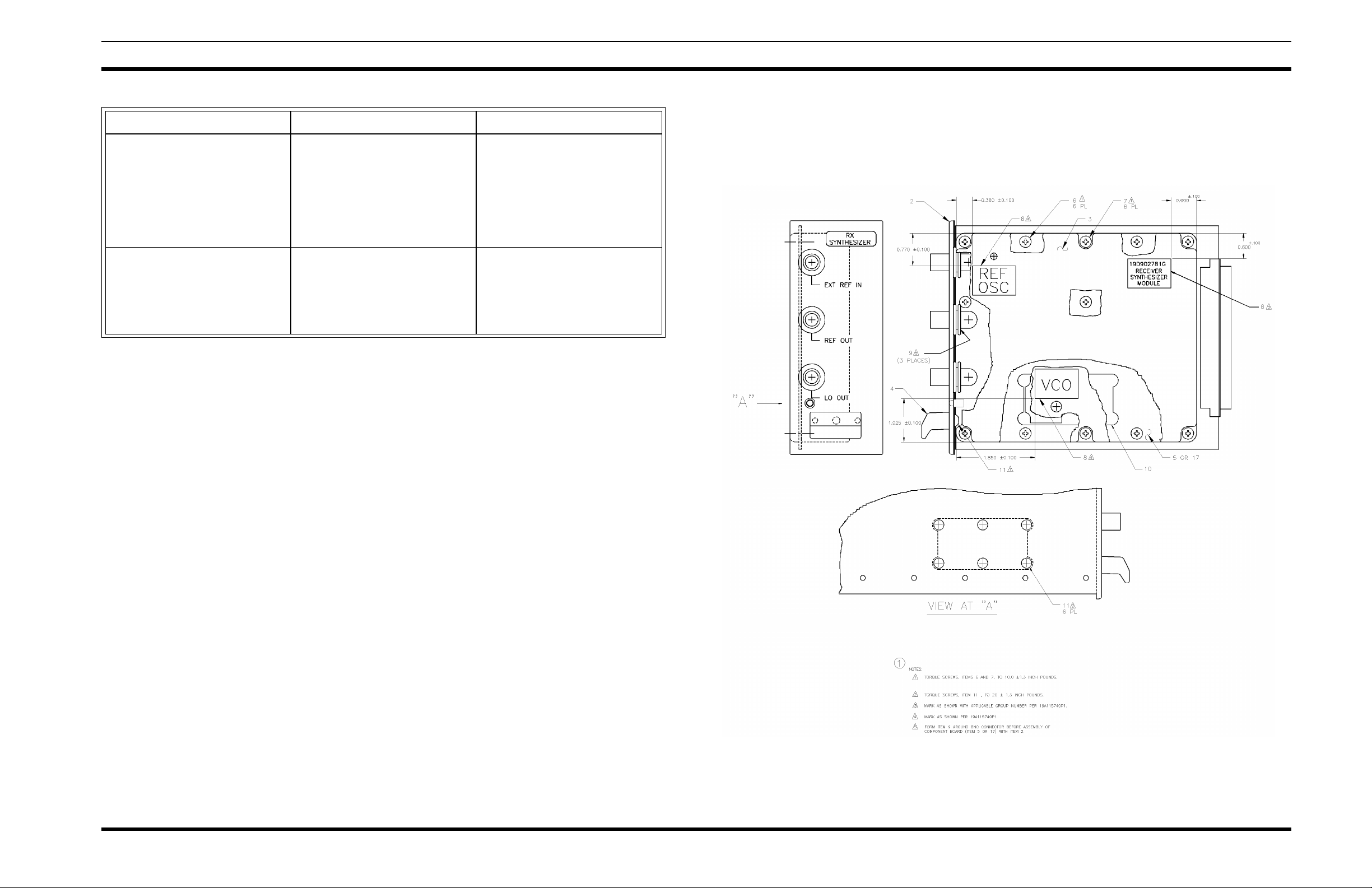
ASSEMBLY DIAGRAM
TROUBLESHOOTING CHART (Con t i nu ed )
SYMPTOM AREAS TO CHECK INDICATIONS
III. LO power low or tuned out of
band.
IV. LO signal not present. (i.e. Q1
does not oscillate)
1. Check tuning with 6 Vdc
applied using test procedure.
F
5 MHz
±
LO
2. Check DC bias at Buffer
Amplifiers U1, U2, & U3 pin 3
Typ. 3.2 Vdc.
1. Check DC bias at Q1 drai n .
(Typ. +8Vdc)
2. Check DC bias at Q1 source.
(Typ. +0.9 Vdc)
LO tuning incorrect. Retune
following test proc ed ure.
Bad Buffer Amplifier. Replace bad
part.
Replace Q 1 .
RECEIVER SYNTHESIZER MODULE
19D902781G1 & G2
(19D902781, Sh1, Rev. 7)
4
 Loading...